ICGOO在线商城 > 射频/IF 和 RFID > RF 检测器 > ADL5513ACPZ-R7
 Datasheet下载
- 型号: ADL5513ACPZ-R7
- 制造商: Analog
- 库位|库存: xxxx|xxxx
- 要求:
| 数量阶梯 | 香港交货 | 国内含税 |
| +xxxx | $xxxx | ¥xxxx |
查看当月历史价格
查看今年历史价格
ADL5513ACPZ-R7产品简介:
ICGOO电子元器件商城为您提供ADL5513ACPZ-R7由Analog设计生产,在icgoo商城现货销售,并且可以通过原厂、代理商等渠道进行代购。 ADL5513ACPZ-R7价格参考¥129.95-¥155.94。AnalogADL5513ACPZ-R7封装/规格:RF 检测器, RF Detector IC WiMax, WLAN 1MHz ~ 4GHz -58dBm ~ 6dBm ±0.5dB 16-VFQFN Exposed Pad, CSP。您可以下载ADL5513ACPZ-R7参考资料、Datasheet数据手册功能说明书,资料中有ADL5513ACPZ-R7 详细功能的应用电路图电压和使用方法及教程。
ADL5513ACPZ-R7是Analog Devices Inc.推出的一款高性能RF检波器,广泛应用于需要精确射频功率检测的场合。该器件可在40MHz至6GHz的宽频率范围内工作,适用于多频段无线通信系统。其主要应用场景包括无线基础设施中的基站功率控制与监测,如GSM、CDMA、WCDMA、LTE及5G通信系统,用于实现发射信号的动态功率调节和自动电平控制(ALC),确保信号传输稳定并符合法规要求。

此外,ADL5513ACPZ-R7也常用于便携式和固定式无线设备中的RF功率测量,例如在点对点微波链路、卫星通信和雷达系统中进行信号强度检测与反馈控制。其高线性度、宽动态范围(可达60dB以上)以及温度稳定性,使其在环境变化较大的工业应用中表现出色。该器件采用紧凑的16引脚LFCSP封装,适合空间受限的高密度电路板设计。

由于其响应速度快、功耗低,ADL5513ACPZ-R7还适用于电池供电的测试仪器和现场可编程门阵列(FPGA)或数字信号处理器(DSP)配合使用的闭环功率控制系统。总体而言,这款RF检波器凭借其宽带性能和高精度,在现代射频系统中发挥着关键作用。
| 参数 | 数值 |
| 产品目录 | |
| 描述 | IC LOG DETECTOR/CTRLR 16 LFCSP对数放大器 1MHz-4GHz 80 dB |
| 产品分类 | |
| 品牌 | Analog Devices Inc |
| 产品手册 | |
| 产品图片 |
|
| rohs | 符合RoHS无铅 / 符合限制有害物质指令(RoHS)规范要求 |
| 产品系列 | 放大器 IC,对数放大器,Analog Devices ADL5513ACPZ-R7- |
| 数据手册 | |
| 产品型号 | ADL5513ACPZ-R7 |
| PCN其它 | |
| RF类型 | WiMax,WLAN |
| 产品 | Logarithmic Amplifiers |
| 产品培训模块 | http://www.digikey.cn/PTM/IndividualPTM.page?site=cn&lang=zhs&ptm=25139 |
| 产品目录页面 | |
| 产品种类 | 对数放大器 |
| 其它名称 | ADL5513ACPZ-R7DKR |
| 功率耗散 | 220 mW |
| 包装 | Digi-Reel® |
| 商标 | Analog Devices |
| 安装风格 | SMD/SMT |
| 封装 | Reel |
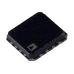
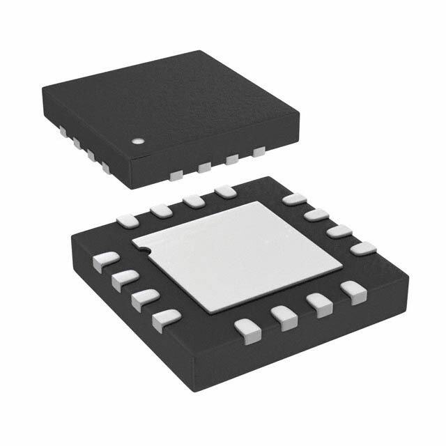
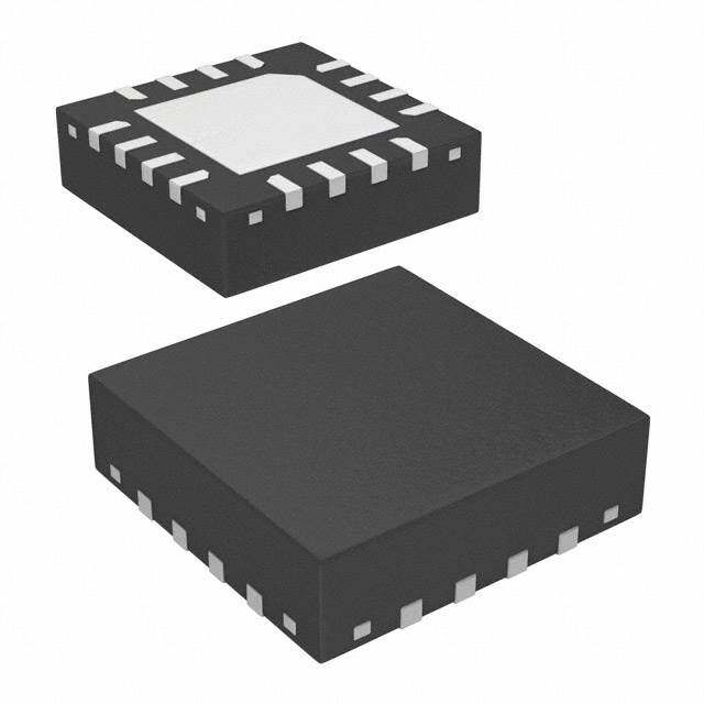
| 封装/外壳 | 16-VFQFN 裸露焊盘,CSP |
| 封装/箱体 | LFCSP-16 |
| 工作温度范围 | - 40 C to + 125 C |
| 工作电源电压 | 2.7 V to 5.5 V |
| 工厂包装数量 | 1500 |
| 带宽 | 1 MHz to 4 GHz |
| 放大器类型 | Logarithmic |
| 最小工作温度 | - 40 C |
| 标准包装 | 1 |
| 电压-电源 | 2.7 V ~ 5.5 V |
| 电流-电源 | 31mA |
| 电源电流 | 31 mA |
| 类型 | Log Amp Detector |
| 精度 | ±0.5dB |
| 系列 | ADL5513 |
| 视频文件 | http://www.digikey.cn/classic/video.aspx?PlayerID=1364138032001&width=640&height=505&videoID=2245193150001 |
| 设计资源 | |
| 输入电压范围—最大 | 5.5 V |
| 输入范围 | -58dBm ~ 6dBm |
| 通道数量 | 1 Channel |
| 频率 | 1MHz ~ 4GHz |


- 商务部:美国ITC正式对集成电路等产品启动337调查
- 曝三星4nm工艺存在良率问题 高通将骁龙8 Gen1或转产台积电
- 太阳诱电将投资9.5亿元在常州建新厂生产MLCC 预计2023年完工
- 英特尔发布欧洲新工厂建设计划 深化IDM 2.0 战略
- 台积电先进制程称霸业界 有大客户加持明年业绩稳了
- 达到5530亿美元!SIA预计今年全球半导体销售额将创下新高
- 英特尔拟将自动驾驶子公司Mobileye上市 估值或超500亿美元
- 三星加码芯片和SET,合并消费电子和移动部门,撤换高东真等 CEO
- 三星电子宣布重大人事变动 还合并消费电子和移动部门
- 海关总署:前11个月进口集成电路产品价值2.52万亿元 增长14.8%


PDF Datasheet 数据手册内容提取
1 MHz to 4 GHz, 80 dB Logarithmic Detector/Controller Data Sheet ADL5513 FEATURES FUNCTIONAL BLOCK DIAGRAM Wide bandwidth: 1 MHz to 4 GHz NC NC CLPF NC 16 15 14 13 80 dB dynamic range (±3 dB) Constant dynamic range over frequency DET DET DET DET DET I V 12 VOUT Stability over −40oC to +85oC temperature range: ±0.5 dB VPOS 1 Operating temperature range: −40oC to +125oC INHI 2 Sensitivity: −70 dBm I V 11 VSET INLO 3 Low noise measurement/controller output (VOUT) ADL5513 Pulse response time: 21 ns/20 ns (fall/rise) 10 COMM Single-supply operation: 2.7 V to 5.5 V at 31 mA VPOS 4 SLOPE BAND GAP GAIN CONTROL REFERENCE BIAS 9 TADJ PSmowaellr f-odootwpnri nfeta LtFuCreS:P 1 mW at 5 V N5C N6C N7C N8C 07514-001 Fabricated using high speed SiGe process Figure 1. APPLICATIONS RF transmitter power amplifier linearization and gain/power control Power monitoring in radio link transmitters RSSI measurement in base stations, WLAN, WiMAX, RADAR GENERAL DESCRIPTION The ADL5513 is a demodulating logarithmic amplifier, capable The feedback loop through an RF amplifier is closed via VOUT, of accurately converting an RF input signal to a corresponding the output of which regulates the amplifier output to a magni- decibel-scaled output. It employs the progressive compression tude corresponding to VSET. The ADL5513 provides 0 V to technique over a cascaded amplifier chain, each stage of which (V − 0.1 V) output capability at the VOUT pin, suitable POS is equipped with a detector cell. The device can be used in either for controller applications. As a measurement device, VOUT measurement or controller modes. The ADL5513 maintains is externally connected to VSET to produce an output voltage, accurate log conformance for signals up to 4 GHz. The input V , that increases linear-in-dB with RF input signal amplitude. OUT dynamic range is typically 80 dB (referred to 50 Ω) with error less The logarithmic slope is 21 mV/dB, determined by the VSET than ±3 dB and 74 dB with error less than ±1 dB. The ADL5513 interface. The intercept is −88 dBm (referred to 50 Ω, conti- has 20 ns response time that enables RF burst detection to a nuous wave input, 900 MHz) using the INHI input. These pulse rate of beyond 50 MHz. The device provides unprecedented parameters are very stable against supply and temperature logarithmic intercept stability vs. ambient temperature conditions. variations. A supply of 2.7 V to 5.5 V is required to power the device. Current The ADL5513 is fabricated on a SiGe bipolar IC process and consumption is 31 mA, and it decreases to 200 μA when the is available in a 3 mm × 3 mm, 16-lead LFCSP package for the device is disabled. −40°C to +125°C operating temperature range. A fully populated The ADL5513 can be configured to provide a control voltage to evaluation board is available. a power amplifier or a measurement output from the VOUT pin. Because the output can be used for controller applications, special attention has been paid to minimize wideband noise. In this mode, the setpoint control voltage is applied to the VSET pin. Rev. A Document Feedback Information furnished by Analog Devices is believed to be accurate and reliable. However, no responsibility is assumed by Analog Devices for its use, nor for any infringements of patents or other One Technology Way, P.O. Box 9106, Norwood, MA 02062-9106, U.S.A. rights of third parties that may result from its use. Specifications subject to change without notice. No license is granted by implication or otherwise under any patent or patent rights of Analog Devices. Tel: 781.329.4700 ©2008–2017 Analog Devices, Inc. All rights reserved. Trademarks and registered trademarks are the property of their respective owners. Technical Support www.analog.com
ADL5513 Data Sheet TABLE OF CONTENTS Features .............................................................................................. 1 Setpoint Interface ....................................................................... 15 Applications ....................................................................................... 1 Description of Characterization ............................................... 15 Functional Block Diagram .............................................................. 1 Error Calculations ...................................................................... 16 General Description ......................................................................... 1 Adjusting Accuracy Through Choice of Calibration Points 16 Revision History ............................................................................... 2 Temperature Compensation of Output Voltage ..................... 17 Specifications ..................................................................................... 3 Device Calibration ..................................................................... 18 Absolute Maximum Ratings ............................................................ 7 Power-Down Functionality ....................................................... 18 ESD Caution .................................................................................. 7 Measurement Mode ................................................................... 19 Pin Configuration and Function Descriptions ............................. 8 Setting the Output Slope in Measurement Mode .................. 19 Typical Performance Characteristics ............................................. 9 Controller Mode ......................................................................... 20 Theory of Operation ...................................................................... 13 Constant Power Operation ....................................................... 20 Applications Information .............................................................. 14 Increasing the Dynamic Range of the ADL5513 ................... 22 Basic Connections ...................................................................... 14 Evaluation Board ............................................................................ 23 Input Signal Coupling ................................................................ 14 Outline Dimensions ....................................................................... 25 Output Filtering .......................................................................... 14 Ordering Guide .......................................................................... 25 Output Interface ......................................................................... 15 REVISION HISTORY 8/2017—Rev. 0 to Rev. A Change to Figure 2 ........................................................................... 8 Updated Outline Dimensions ...................................................... 25 Changes to Ordering Guide .......................................................... 25 10/2008—Revision 0: Initial Version Rev. A | Page 2 of 25
Data Sheet ADL5513 SPECIFICATIONS VS = 5 V, TA = 25°C, Z0 = 50 Ω, Pin INHI and Pin INLO are ac-coupled, continuous wave (CW) input, single-ended input drive, VOUT tied to VSET, error referred to best-fit line (linear regression −20 to −40 dBm), unless otherwise noted. (Temperature adjust voltage optimized for 85°C.) Table 1. Parameter Conditions Min Typ Max Unit OVERALL FUNCTION Maximum Input Frequency 1 4000 MHz FREQUENCY = 100 MHz Output Voltage: High Power Input P = −10 dBm 1.50 1.63 1.76 V IN Output Voltage: Low Power Input P = −50 dBm 0.64 0.79 0.94 V IN ±3.0 dB Dynamic Range 75 dB ±1.0 dB Dynamic Range 64 dB ±0.5 dB Dynamic Range 58 dB Maximum Input Level, ±1.0 dB 6 dBm Minimum Input Level, ±1.0 dB −58 dBm Deviation at TA = 25°C PIN = −10 dBm 0.27 dB P = −30 dBm 0.003 dB IN P = −50 dBm −0.14 dB IN Deviation vs. Temperature Deviation from output at TA = 25°C 25°C < T < 85°C; P = −10 dBm +0.15/−0.33 dB A IN −40°C < T < +25°C; P = −10 dBm +0.23/−0.43 dB A IN 25°C < T < 125°C; P = −10 dBm 0.8 dB A IN 25°C < T < 85°C; P = −30 dBm +0.12/−0.31 dB A IN −40°C < T < +25°C; P = −30 dBm ±0.31 dB A IN 25°C < T < 125°C; P = −30 dBm +0.74 dB A IN +25°C < T < +85°C; P = −50 dBm +0.35/−0.18 dB A IN −40°C < T < +25°C; P = −50 dBm +0.25/−0.47 dB A IN 25°C < T < 125°C; P = −50 dBm +0.52/−0.24 dB A IN Logarithmic Slope 19.5 21 22.5 mV/dB Logarithmic Intercept −87 dBm Input Impedance 1.3/0.4 kΩ/pF FREQUENCY = 900 MHz Output Voltage: High Power Input P = −10 dBm 1.64 V IN Output Voltage: Low Power Input P = −50 dBm 0.79 V IN ±3.0 dB Dynamic Range 76 dB ±1.0 dB Dynamic Range 70 dB ±0.5 dB Dynamic Range 68 dB Maximum Input Level, ±1.0 dB 8 dBm Minimum Input Level, ±1.0 dB −62 dBm Deviation at TA = 25°C PIN = −10 dBm 0.2 dB P = −30 dBm 0.002 dB IN P = −50 dBm 0.34 dB IN Deviation vs. Temperature Deviation from output at TA = 25°C 25°C < T < 85°C; P = −10 dBm +0.25/−0.3 dB A IN −40°C < T < +25°C; P = −10 dBm +0.2/−0.53 dB A IN 25°C < T < 125°C; P = −10 dBm +0.72/−0.1 dB A IN 25°C < T < 85°C; P = −30 dBm +0.2/−0.3 dB A IN −40°C < T < +25°C; P = −30 dBm +0.28/−0.37 dB A IN 25°C < T < 125°C; P = −30 dBm 0.7 dB A IN 25°C < T < 85°C; P = −50 dBm +0.4/−0.36 dB A IN −40°C < T < +25°C; P = −50 dBm +0.37/−0.5 dB A IN 25°C < T < 125°C; P = −50 dBm +0.67/−0.28 dB A IN Rev. A | Page 3 of 25
ADL5513 Data Sheet Parameter Conditions Min Typ Max Unit Logarithmic Slope 21 mV/dB Logarithmic Intercept −88 dBm Input Impedance 1.3/0.4 kΩ/pF FREQUENCY = 1900 MHz Output Voltage: High Power Input P = −10 dBm 1.66 V IN Output Voltage: Low Power Input P = −50 dBm 0.80 V IN ±3.0 dB Dynamic Range 75 dB ±1.0 dB Dynamic Range 70 dB ±0.5 dB Dynamic Range 68 dB Maximum Input Level, ±1.0 dB 8 dBm Minimum Input Level, ±1.0 dB −62 dBm Deviation at TA = 25°C PIN = −10 dBm 0.25 dB P = −30 dBm 0.0012 dB IN P = −50 dBm 0.52 dB IN Deviation vs. Temperature Deviation from output at TA = 25°C 25°C < T < 85°C; P = −10 dBm +0.14/−0.41 dB A IN −40°C < T < +25°C; P = −10 dBm +0.19/−0.51 dB A IN 25°C < T < 125°C; P = −10 dBm 0.9 dB A IN 25°C < T < 85°C; P = −30 dBm +0.1/−0.38 dB A IN −40°C < T < +25°C; P = −30 dBm +0.37/−0.26 dB A IN 25°C < T < 125°C; P = −30 dBm 0.83 dB A IN 25°C < T < 85°C; P = −50 dBm +0.55/−0.3 dB A IN −40°C < T < +25°C; P = −50 dBm +0.79/−0.16 dB A IN 25°C < T < 125°C; P = −50 dBm +0.62/−0.41 dB A IN Logarithmic Slope 21 mV/dB Logarithmic Intercept −88 dBm Input Impedance 0.6/0.5 kΩ/pF FREQUENCY = 2140 MHz Output Voltage: High Power Input P = −10 dBm 1.66 V IN Output Voltage: Low Power Input P = −50 dBm 0.82 V IN ±3.0 dB Dynamic Range 77 dB ±1.0 dB Dynamic Range 70 dB ±0.5 dB Dynamic Range 66 dB Maximum Input Level, ±1.0 dB 8 dBm Minimum Input Level, ±1.0 dB −62 dBm Deviation at TA = 25°C PIN = −10 dBm 0.33 dB P = −30 dBm 0.02 dB IN P = −50 dBm 0.23 dB IN Deviation vs. Temperature Deviation from output at TA = 25°C 25°C < T < 85°C; P = −10 dBm ±0.28 dB A IN −40°C < T < +25°C; P = −10 dBm +0.2/−0.52 dB A IN 25°C < T < 125°C; P = −10 dBm +0.7/−0.1 dB A IN 25°C < T < 85°C; P = −30 dBm +0.15/−0.35 dB A IN −40°C < T < +25°C; P = −30 dBm +0.24/−0.41 dB A IN 25°C < T < 125°C; P = −30 dBm 0.77 dB A IN 25°C < T < 85°C; P = −50 dBm +0.2/−0.6 dB A IN −40°C < T < +25°C; P = −50 dBm +0.1/−0.94 dB A IN 25°C < T < 125°C; P = −50 dBm +0.8/−0.2 dB A IN Logarithmic Slope 21 mV/dB Logarithmic Intercept −89 dBm Input Impedance 0.5/0.5 kΩ/pF Rev. A | Page 4 of 25
Data Sheet ADL5513 Parameter Conditions Min Typ Max Unit FREQUENCY = 2600 MHz Output Voltage: High Power Input P = −10 dBm 1.67 V IN Output Voltage: Low Power Input P = −50 dBm 0.83 V IN ±3.0 dB Dynamic Range 80 dB ±1.0 dB Dynamic Range 74 dB ±0.5 dB Dynamic Range 69 dB Maximum Input Level, ±1.0 dB 7 dBm Minimum Input Level, ±1.0 dB −67 dBm Deviation at TA = 25°C PIN = −10 dBm 0.33 dB P = −30 dBm 0.02 dB IN P = −50 dBm 0.01 dB IN Deviation vs. Temperature Deviation from output at TA = 25°C 25°C < T < 85°C; P = −10 dBm +0.2/−0.4 dB A IN −40°C < T < +25°C; P = −10 dBm +0.05/−0.68 dB A IN 25°C < T < 125°C; P = −10 dBm +0.75/−0.05 dB A IN 25°C < T < 85°C; P = −30 dBm +0.1/−0.37 dB A IN −40°C < T < +25°C; P = −30 dBm +0.25/−0.4 dB A IN 25°C < T < 125°C; P = −30 dBm 0.8 dB A IN 25°C < T < 85°C; P = −50 dBm +0.2/−0.6 dB A IN −40°C < T < +25°C; P = −50 dBm ±0.5 dB A IN 25°C < T < 125°C; P = −50 dBm 1.13 dB A IN Logarithmic Slope 21 mV/dB Logarithmic Intercept −89 dBm Input Impedance 0.4/0.6 kΩ/pF FREQUENCY = 3.6 GHz Output Voltage: High Power Input P = −10 dBm 1.74 V IN Output Voltage: Low Power Input P = −50 dBm 0.84 V IN ±3.0 dB Dynamic Range 76 dB ±1.0 dB Dynamic Range 62 dB ±0.5 dB Dynamic Range 58 dB Maximum Input Level, ±1.0 dB 1 dBm Minimum Input Level, ±1.0 dB −61 dBm Deviation at TA = 25°C PIN = −10 dBm 0.43 dB P = −30 dBm −0.05 dB IN P = −50 dBm −0.14 dB IN Deviation vs. Temperature Deviation from output at TA = 25°C 25°C < T < 85°C; P = −10 dBm +0.32/−0.28 dB A IN −40°C < T < +25°C; P = −10 dBm +0.27/−0.54 dB A IN 25°C < T < 125°C; P = −10 dBm +0.58/−0.21 dB A IN 25°C < T < 85°C; P = −30 dBm +0.3/−0.22 dB A IN −40°C < T < +25°C; P = −30 dBm +0.38/−0.33 dB A IN 25°C < T < 125°C; P = −30 dBm +0.67/−0.05 dB A IN 25°C < T < 85°C; P = −50 dBm +0.41/−0.37 dB A IN −40°C < T < +25°C; P = −50 dBm +0.41/−0.62 dB A IN 25°C < T < 125°C; P = −50 dBm +0.8/−0.18 dB A IN Logarithmic Slope 22.5 mV/dB Logarithmic Intercept −87 dBm Input Impedance 0.5/0.4 kΩ/pF SETPOINT INPUT Pin VSET Nominal Range Log conformance error ≤ ±1 dB, RF input = 8 dBm 2 V Log conformance error ≤ ±1 dB, RF input = −62 dBm 0.58 V Logarithmic Scale Factor 47.1 dB/ V Input Impedance 40 kΩ Rev. A | Page 5 of 25
ADL5513 Data Sheet Parameter Conditions Min Typ Max Unit OUTPUT INTERFACE Pin VOUT Voltage Swing V = 0 V, RF input = open 0.47 V SET V = 0.47 V, RF input = open 4.7 V SET Capacitance Drive CLPF = open 47 pF Capacitance Drive CLPF = 20 pF 1 nF Current Source/Sink Output held at 1 V to 1% change 0.64/55 mA Output Noise RF input = 100 MHz, 0 dBm f = 100 kHz, CLPF = open 145 nV/√Hz NOISE f = 100 kHz, CLPF = 1 nF 82 nV/√Hz NOISE PULSE RESPONSE TIME Input level = no signal to 0 dBm, 90% to 10% Fall Time CLPF = open, 1 µs pulse width 21 ns CLPF = open, 500 µs pulse width 5.5 µs Rise Time CLPF = open, 1 µs pulse width 20 ns CLPF = open, 500 µs pulse width 20 ns Fall Time CLPF = 1000 pF, 10 µs pulse width 4.2 µs CLPF = 1000 pF, 500 µs pulse width 5.5 µs Rise Time CLPF = 1000 pF, 10 µs pulse width 3.2 µs CLPF = 1000 pF, 500 µs pulse width 4.3 µs Small Signal Video Bandwidth (or Envelope CLPF = open, 3 dB video bandwidth 10 MHz Bandwidth) TEMPERATURE ADJUST/POWER-DOWN Pin TADJ INTERFACE Temperature Adjust Useful Range 0 to 1.3 V Minimum Logic Level to Disable Logic high disables V − 0.3 V POS Input Current Logic high TADJ = 0 V 31 mA Logic low TADJ = 4.7 V 200 µA Enable Time PWDN low to VOUT at 100% final value, PWDN high to VOUT at 10% final value CLPF = open, RF input = 0 dBm, 100 MHz, 84 ns 1 µs pulse width CLPF = 1000 pF, RF input = 0 dBm, 100 MHz, 10.8 µs 1 µs pulse width Disable Time CLPF = open, RF input = 0 dBm, 100 MHz, 165 ns 1 µs pulse width CLPF = 1000 pF, RF input = 0 dBm, 100 MHz, 1.2 µs 1 µs pulse width Input Impedance1 TADJ = 0.9 V, sourcing 70 µA 13 kΩ POWER SUPPLY INTERFACE Pin VPOS Supply Voltage 2.7 5.5 V Quiescent Current 25°C, RF input = −55 dBm 31 mA Supply Current When disabled <0.2 mA 1 See the Temperature Compensation of Output Voltage section. Rev. A | Page 6 of 25
Data Sheet ADL5513 ABSOLUTE MAXIMUM RATINGS ESD CAUTION Table 2. Parameter Rating Supply Voltage, V 5.5 V POS V Voltage 0 V to V SET POS Input Power (Single-Ended, Re: 50 Ω) 20 dBm Internal Power Dissipation 220 mW θ 79.3°C/W JA Maximum Junction Temperature 150°C Operating Temperature Range −40°C to +125°C Storage Temperature Range −65°C to +150°C Lead Temperature (Soldering, 60 sec) 260°C Stresses at or above those listed under Absolute Maximum Ratings may cause permanent damage to the product. This is a stress rating only; functional operation of the product at these or any other conditions above those indicated in the operational section of this specification is not implied. Operation beyond the maximum operating conditions for extended periods may affect product reliability. Rev. A | Page 7 of 25
ADL5513 Data Sheet PIN CONFIGURATION AND FUNCTION DESCRIPTIONS F P C C L C N N C N 6 5 4 3 1 1 1 1 VPOS 1 12 VOUT INHI 2 ADL5513 11 VSET TOP VIEW INLO 3 (Not to Scale) 10 COMM VPOS 4 9 TADJ 5 6 7 8 C C C C N N N N NOTES 12..NTCAHCO LE NO= N EWNEXO CPIM TOCPEOSEDEND DTNA OEPNC ACCTDEO. MIGSMR INO; TSUEONRLDND PAELLRAL TNYOE. 07514-002 Figure 2. Pin Configuration Table 3. Pin Function Descriptions Pin No. Mnemonic Description 1, 4 VPOS Positive Supply Voltage, 2.7 V to 5.5 V. 2 INHI RF Input. AC-coupled RF input. 3 INLO RF Common for INHI. AC-coupled RF common. 5, 6, 7, 8, NC No Connect. These pins can be left open or be soldered to a low impedance ground plane. 13, 15, 16 9 TADJ Temperature Compensation Adjustment. Frequency-dependent temperature compensation is set by applying a specified voltage to the pin. The TADJ pin has dual functionality as a power-down pin, PWDN. Applying a voltage of V − 0.3 V disables the device. POS 10 COMM Device Common. 11 VSET Setpoint Input for Operation in Controller Mode. To operate in RSSI mode short VSET to VOUT. 12 VOUT Logarithmic/Error Output. 14 CLPF Loop Filter Capacitor Pin. In measurement mode, this capacitor pin sets the pulse response time and video bandwidth. In controller mode, the capacitance on this node sets the response time of the error amplifier/integrator. 15 (EPAD) Exposed Pad Internally connected to COMM; solder to a low impedance ground plane. (EPAD) Rev. A | Page 8 of 25
Data Sheet ADL5513 TYPICAL PERFORMANCE CHARACTERISTICS V = 5 V; T = +25°C, −40°C, +85°C, +125°C; C = 0.1 μF, error is calculated by using the best-fit line between P = −20 dBm and P = POS A LPF IN IN −40 dBm at the specified input frequency, unless otherwise noted. 2.4 3.0 2.4 3.0 2.2 2.5 2.2 2.5 2.0 2.0 2.0 2.0 1.8 1.5 1.8 1.5 1.6 1.0 1.6 1.0 (V)UT11..42 00.5 OR (dB) (V)UT11..42 00.5 OR (dB) O R O R V 1.0 –0.5 R V 1.0 –0.5 R E E 0.8 –1.0 0.8 –1.0 +25°C 0.6 +25°C –1.5 0.6 –40°C –1.5 0.4 –40°C –2.0 0.4 +85°C –2.0 +85°C +125°C 0.2 +125°C –2.5 0.2 –2.5 0–70 –60 –50 –40 PIN –(3d0Bm) –20 –10 0 10–3.0 07514-003 0–70 –60 –50 –40 PIN –(3d0Bm) –20 –10 0 10–3.0 07514-005 Figure 3. VOUT and Log Conformance vs. Input Amplitude at 100 MHz, Figure 6. VOUT and Log Conformance vs. Input Amplitude at 100 MHz, Typical Device, VTADJ = 0.89 V Multiple Devices, VTADJ = 0.89 V 2.4 3.0 2.4 3.0 2.2 2.5 2.2 2.5 2.0 2.0 2.0 2.0 1.8 1.5 1.8 1.5 1.6 1.0 1.6 1.0 (V)UT11..42 00.5 OR (dB) (V)UT11..42 00.5 OR (dB) O R O R V 1.0 –0.5 R V 1.0 –0.5 R E E 0.8 –1.0 0.8 –1.0 +25°C 0.6 +25°C –1.5 0.6 –40°C –1.5 0.4 –+4805°°CC –2.0 0.4 ++8152°5C°C –2.0 0.2 +125°C –2.5 0.2 –2.5 0–70 –60 –50 –40 PIN–(d30Bm) –20 –10 0 10–3.0 07514-004 0–70 –60 –50 –40 PIN –(3d0Bm) –20 –10 0 10–3.0 07514-006 Figure 4. VOUT and Log Conformance vs. Input Amplitude at 900 MHz, Figure 7. VOUT and Log Conformance vs. Input Amplitude at 900 MHz, Typical Device, VTADJ = 0.86 V Multiple Devices, VTADJ = 0.86 V 2.4 3.0 2.4 3.0 2.2 2.5 2.2 2.5 2.0 2.0 2.0 2.0 1.8 1.5 1.8 1.5 1.6 1.0 1.6 1.0 (V)UT11..42 00.5 OR (dB) (V)UT11..42 00.5 OR (dB) O R O R V 1.0 –0.5 R V 1.0 –0.5 R E E 0.8 –1.0 0.8 –1.0 +25°C 0.6 +25°C –1.5 0.6 –40°C –1.5 0.4 –40°C –2.0 0.4 +85°C –2.0 +85°C 125°C 0.2 +125°C –2.5 0.2 –2.5 0–70 –60 –50 –40 PIN –(3d0Bm) –20 –10 0 10–3.0 07514-007 0–70 –60 –50 –40 PIN –(3d0Bm) –20 –10 0 10–3.0 07514-010 Figure 5. VOUT and Log Conformance vs. Input Amplitude at 1900 MHz, Figure 8. VOUT and Log Conformance vs. Input Amplitude at 1900 MHz, Typical Device, VTADJ = 0.80 V Multiple Devices, VTADJ = 0.80 V Rev. A | Page 9 of 25
ADL5513 Data Sheet 2.4 3.0 2.4 3.0 2.2 2.5 2.2 2.5 2.0 2.0 2.0 2.0 1.8 1.5 1.8 1.5 1.6 1.0 1.6 1.0 (V)UT11..42 00.5 OR (dB) (V)UT11..42 00.5 OR (dB) O R O R V 1.0 –0.5 R V 1.0 –0.5 R E E 0.8 –1.0 0.8 –1.0 +25°C 0.6 +25°C –1.5 0.6 –40°C –1.5 0.4 –+4805°°CC –2.0 0.4 +12855°°CC –2.0 0.2 125°C –2.5 0.2 –2.5 0–70 –60 –50 –40 PIN –(3d0Bm) –20 –10 0 10–3.0 07514-008 0–70 –60 –50 –40 PIN –(3d0Bm) –20 –10 0 10–3.0 07514-011 Figure 9. VOUT and Log Conformance vs. Input Amplitude at 2140 MHz, Figure 12. VOUT and Log Conformance vs. Input Amplitude at 2140 MHz, Typical Device, VTADJ = 0.84 V Multiple Devices, VTADJ = 0.84 V 2.4 3.0 2.4 3.0 2.2 2.5 2.2 2.5 2.0 2.0 2.0 2.0 1.8 1.5 1.8 1.5 1.6 1.0 1.6 1.0 (V)UT11..42 00.5 OR (dB) (V)UT11..42 00.5 OR (dB) O R O R V 1.0 –0.5 R V 1.0 –0.5 R E E 0.8 –1.0 0.8 –1.0 +25°C 0.6 +25°C –1.5 0.6 –40°C –1.5 0.4 –40°C –2.0 0.4 +85°C –2.0 +85°C 125°C 0.2 125°C –2.5 0.2 –2.5 0–70 –60 –50 –40 PIN –(3d0Bm) –20 –10 0 10–3.0 07514-009 0–70 –60 –50 –40 PIN –(3d0Bm) –20 –10 0 10–3.0 07514-012 Figure 10. VOUT and Log Conformance vs. Input Amplitude at 2600 MHz, Figure 13. VOUT and Log Conformance vs. Input Amplitude at 2600 MHz, Typical Device, VTADJ = 0.83 V Multiple Devices, VTADJ = 0.83 V 2.4 3.0 2.4 3.0 2.2 2.5 2.2 2.5 2.0 2.0 2.0 2.0 1.8 1.5 1.8 1.5 1.6 1.0 1.6 1.0 (V)UT11..42 00.5 OR (dB) (V)UT11..42 00.5 OR (dB) O R O R V 1.0 –0.5 R V 1.0 –0.5 R E E 0.8 –1.0 0.8 –1.0 +25°C 0.6 +25°C –1.5 0.6 –40°C –1.5 0.4 –+4805°°CC –2.0 0.4 +12855°°CC –2.0 0.2 125°C –2.5 0.2 –2.5 0–70 –60 –50 –40 PIN –(3d0Bm) –20 –10 0 10–3.0 07514-013 0–70 –60 –50 –40 PIN –(3d0Bm) –20 –10 0 10–3.0 07514-016 Figure 11. VOUT and LoTgy Cpiocnaflo Drmevaicnec, eV vTAsD. JI n=p 0u.9t 0A mV plitude at 3600 MHz, Figure 14. VOUT and LMogu lCtiopnlefo Drmevaicnecse, VvTsA. DInJ =p u0t. 9A0m Vp litude at 3600 MHz, Rev. A | Page 10 of 25
Data Sheet ADL5513 100k 100k PIN = 0dBm PIN = 0dBm PIN = –10dBm PIN = –10dBm NOISE SPECTRAL DENSITY (nV/Hz) 11001k0k PPPPIIIINNNN ==== –––O246F000FdddBBBmmm NOISE SPECTRAL DENSITY (nV/Hz) 11001k0k PPPPIIIINNNN ==== –––O246F000FdddBBBmmm 101k 10k FREQU1E0N0kCY (Hz) 1M 10M 07514-015 101k 10k FREQU1E0N0kCY (Hz) 1M 10M 07514-018 Figure 15. Output Noise Spectral Density, CLPF = Open Figure 18. Output Noise Spectral Density, CLPF = 1 nF 2.4 6 2.4 6 2.2 RF PULSE 2.2 PIN = 0dBm 2.0 PIN = –10dBm 5 2.0 RF PULSE 5 1.8 PIN = –20dBm 1.8 PIN = 0dBm V (V)OUT 11110.....64208 PPPPIIIINNNN ==== ––––34560000ddddBBBBmmmm 432 INPUT PULSE (V) V (V)OUT 11110.....64208 PPPPPIIIIINNNNN ===== –––––1235400000dddddBBBBBmmmmm 432 INPUT PULSE (V) 0.6 0.6 0.4 1 0.4 PIN = –60dBm 1 0.2 0.2 00100200300400 500600 700 800T900IME1000 (n1100s)12001300 1400 150016001700 18001900 20000 07514-019 00 10 20 30 TIME4 0(ms) 50 60 70 800 07514-020 Figure 16. Output Response to RF Burst Input for Various RF Input Levels, Figure 19. Output Response to RF Burst Input for Various RF Input Levels, Carrier Frequency = 100 MHz, CLPF = Open Carrier Frequency = 100 MHz, CLPF = 0.1 μF 1.8 5 1.8 5 1.6 1.6 1.4 4 1.4 4 V (V)OUT11000.....20864 PPPPPPPPOIIIIIIINNNNNNNW ======= E0––––––Rd123456000000-BDddddddmOBBBBBBWmmmmmmN PULSE 32 OWER-DOWN PULSE (V) V (V)OUT10001.....20864 PPPPPPPPIIIIOIIINNNNNNNW ======= E–0–––––R3456d12000000-BDddddddmOBBBBBBWmmmmmmN PULSE 32 OWER-DOWN PULSE (V) P P 0.2 1 0.2 1 0 0 –0.20 100 200 300 TIME400 (µs) 500 600 700 8000 07514-022 –0.20 100 200 300 T400IME (µ500s) 600 700 800 9000 07514-021 Figure 17. Output Response Using Power-Down Mode for Various RF Input Figure 20. Output Response Using Power-Down Mode for Various RF Input Levels, Carrier Frequency = 100 MHz, CLPF = Open Levels, Carrier Frequency = 100 MHz, CLPF = 10 pF Rev. A | Page 11 of 25
ADL5513 Data Sheet 2.4 3.0 1600 MEAN = 21.0268 2.2 2.5 1400 2.0 2.0 1.8 1.5 1200 1.6 1.0 1000 V (V)OUT 111...420 00–.05.5 RROR (dB) COUNT 800 E 600 0.8 –1.0 0.6 +25°C –1.5 400 –40°C 0.4 –2.0 +85°C 200 0.2 +125°C –2.5 0–70–65–60–55–50–45–40–P3I5N –(3d0B–m2)5–20–15–10 –5 0 5 10–3.0 07514-017 109.5 20.0SLOPE2 0@.5 5V/1002M1H.0z @ 25°2C1 .(5mV/dB)22.0 22.5 07514-056 Figure 21. Output Voltage Stability vs. Input Amplitude at 1900 MHz When Figure 23. Slope Distribution, 100 MHz VPOS Varies from 2.7 V to 5.5 V j1 j0.5 j2 100MHz 1/3 1 3 0 900MHz 1900MHz 2140MHz 2600MHz –j0.5 –j2 –j13600MHz 07514-014 Figure 22. Input Impedance vs. Frequency, No Termination Resistor on INHI, Z0 = 50 Ω Rev. A | Page 12 of 25
Data Sheet ADL5513 THEORY OF OPERATION The ADL5513 is a demodulating logarithmic amplifier, specifi- The logarithmic function is approximated in a piecewise cally designed for use in RF measurement and power control fashion by cascaded gain stages. (For a more comprehensive applications at frequencies up to 4 GHz. A block diagram is explanation of the logarithm approximation, see the AD8307 shown in Figure 24. Sharing much of its design with the AD8313 data sheet.) Using precision biasing, the gain is stabilized over logarithmic detector/controller, the ADL5513 maintains tight temperature and supply variations. The overall dc gain is high, intercept variability vs. temperature over a 80 dB range. Additional due to the cascaded nature of the gain stages. enhancements over the AD8313, such as a reduced RF burst The RF signal voltages are converted to a fluctuating differential response time of 20 ns and board space requirements of only current having an average value that increases with signal level. 3 mm × 3 mm, add to the low cost and high performance After the detector currents are summed and filtered, the following benefits found in the ADL5513. function is formed at the summing node: NC NC CLPF NC 16 15 14 13 ID × log10(VIN/VINTERCEPT) (1) where: DET DET DET DET DET I V 12 VOUT I is the internally set detector current. VPOS 1 D V is the input signal voltage. IN INHI 2 I V 11 VSET VINTERCEPT is the intercept voltage (that is, when VIN = VINTERCEPT, INLO 3 the output voltage is 0 V, if it were capable of going to 0). ADL5513 10 COMM VPOS 4 SLOPE BAND GAP GAIN CONTROL REFERENCE BIAS 9 TADJ N5C N6C N7C N8C 07514-024 Figure 24. Block Diagram A fully differential design, using a proprietary, high speed SiGe process, extends high frequency performance. The maximum input with ±1 dB log conformance error is typically 10 dBm (referred to 50 Ω). The noise spectral density of −70 dBm sets the lower limit of the dynamic range. The common pin, COMM, provides a quality low impedance connection to the printed circuit board (PCB) ground. The package paddle, which is internally connected to the COMM pin, should also be grounded to the PCB to reduce thermal impedance from the die to the PCB. Rev. A | Page 13 of 25
ADL5513 Data Sheet APPLICATIONS INFORMATION BASIC CONNECTIONS While the input can be reactively matched, in general, this is not necessary. An external 52.3 Ω shunt resistor (connected to The ADL5513 is specified for operation up to 4 GHz; as a result, the signal side of the input coupling capacitors, as shown in low impedance supply pins with adequate isolation between Figure 25) combines with relatively high input impedance to functions are essential. A power supply voltage of between 2.7 V give an adequate broadband 50 Ω match. and 5.5 V should be applied to VPOS. Connect 100 pF and 0.1 µF The coupling time constant, 50 × C /2, forms a high-pass power supply decoupling capacitors close to this power supply pin. C corner with a 3 dB attenuation at f = 1/(2π × 50 × C ), where VPOS HP C C1 = C2 = C . Using the typical value of 47 nF, this high-pass C C3 (SEE NOTE 1) corner is ~68 kHz. In high frequency applications, fHP should be 0.1µF R11 as large as possible to minimize the coupling of unwanted low 0Ω frequency signals. In low frequency applications, a simple RC C4 100pF 6 5 4 3 network forming a low-pass filter should be added at the input 1 1 1 1 C1 VPOS 1 CN CN FPL CN 12 VOUT VOUT for similar reasons. This low-pass filter network should generally be RFIN 47nF C R4 placed at the generator side of the coupling capacitors, thereby 2INHI VSET11 0Ω R1 ADL5513 lowering the required capacitance value for a given high-pass 52.3Ω C2 3INLO COMM10 corner frequency. 47nF VPOS 4 9 (SEE NOTE 2) C C C C TADJ OUTPUT FILTERING N N N N C5 5 6 7 8 100pF For applications in which maximum video bandwidth and, R12 0Ω Z1 consequently, fast rise time are desired, it is essential that the C6 CLPF pin be left unconnected and free of any stray capacitance. 0.1µF The output video bandwidth, which is 10 MHz, can be reduced by VPOS connecting a ground-referenced capacitor (C ) to the CLPF pin, NOTES FLT 12.. ASSNEEEED TTPHHOEEW OTEEURMT-DPPOEUWRT ANFTI LFUTURENERC CITNOIGOM NSPAEELCNITTSIYAO TSNIE.OCNT OIOFN OSU.TPUT VOLTAGE 07514-025 raisp sphleo w(ant tinw iFcieg uthree i2n7p. uTth firse iqsu geennceyr afollry ad soynme mtoe rterdicu icnep ouut twpuavt e- Figure 25. Basic Connections form such as sinusoidal signals). The exposed paddle of the LFCSP package is internally connected to COMM. For optimum thermal and electrical performance, ILOG solder the paddle to a low impedance ground plane. VOUT +4 INPUT SIGNAL COUPLING 1kΩ 3pF CLPF ITNhLe OR F(i innppuutt c (oImNHmIo)n i)s sshinogulled- ebned aecd- caonudp mleuds tto b ger aocu-ncdou. pled. CFLT 07514-027 Suggested coupling capacitors are 47 nF, ceramic, 0402-style Figure 27. Lowering the Postdemodulation Bandwidth capacitors for input frequencies of 1 MHz to 4 GHz. The C is selected by FLT coupling capacitors should be mounted close to the INHI and 1 INLO pins. The coupling capacitor values can be increased to C = ( ) − 3.0pF lower the high-pass cutoff frequency of the input stage. The high- FLT 2π×1.5kΩ×VideoBandwidth pass corner is set by the input coupling capacitors and the The video bandwidth should typically be set to a frequency internal 20 pF high-pass capacitor. The dc voltage on INHI equal to about one-tenth the minimum input frequency. This and INLO is about one diode voltage drop below VPOS. ensures that the output ripple of the demodulated log output, VPOS which is at twice the input frequency, is well filtered. 7kΩ 7kΩ 20pF In many log amp applications, it may be necessary to lower the corner frequency of the postdemodulation filter to achieve low 15kΩ 15kΩ output ripple while maintaining a rapid response time to changes INHI in signal level. An example of a four-pole active filter is shown GAIN 2kΩ STAGE in the AD8307 data sheet. Averaging the output measurement INLO can also be done when filtering is not possible. OFFSEgTm COMP 07514-026 Figure 26. Input Interface Rev. A | Page 14 of 25
Data Sheet ADL5513 OUTPUT INTERFACE 20kΩ VSET VSET ISET The VOUT pin is driven by a PNP output stage. An internal 10 Ω resistor is placed in series with the output and the VOUT pin. 20kΩ TChLeP Fri.s Te htiem fael ol ft itmhee oisu atpnu Rt Cis- lliimmiitteedd msleawin glyiv beyn tbhye tshleew lo oand COMM 3.5kCΩOMM 07514-029 capacitance and the pull-down resistance at VOUT. There is an Figure 29. VSET Interface internal pull-down resistor of 1.6 kΩ. A resistive load at VOUT is placed in parallel with the internal pull-down resistor to The slope is given by ID × 2x × 3.5 kΩ = 20 mV/dB × x. For provide additional discharge current. example, if a resistor divider to ground is used to generate a VSET voltage of V /2, then x = 2. The slope is set to 800 V/decade VPOS OUT or 40 mV/dB. See the Measurement Mode section for more CLPF 10Ω information on setting the slope in measurement mode. + VOUT 0.8V 1200Ω DESCRIPTION OF CHARACTERIZATION – COMM 400Ω 07514-028 TAhDeL g5e5n1e3r aclh haarardctwerairzea ctioonnf iigs usrhaotwionn iuns eFdig fuorre m 30o.s Tt ohfe t shieg nal Figure 28. Output Interface source and power supply used in this example are the Agilent The ADL5513 output can drive over 1 nF of capacitance. When E8251A PSG signal generator and E3631A triple output power driving such high output capacitive loads, it is required to capaci- supply. Output voltage was measured using the Agilent 34980A tively load the CLPF pin. The capacitance on the CLPF pin switch box. should be at least 1/50th that of the capacitance on the VOUT pin. AGILENT E3631A VPOS SETPOINT INTERFACE TRIPLE OUTPUT POWER SUPPLY ADL5513 The V input drives the high impedance (40 kΩ) input of an CHARACTERIZATION VOUT AGILENT 34980A internaSElT op amp. The VSET voltage appears across the internal AGPISLGEN STI GEN82A5L1A INHI BOARD SWITCH BOX GENERATOR 3.5 kΩ resistor to generate ISET. When a portion of VOUT is applied INLO to VSET, the feedback loop forces If V ID =× Vlog10(/2VxIN, /IVIN T=E RVCEPT) /=(2 IxS E×T 3.5 kΩ). (2) COCNOTMRPOULTLEIRNG 07514-030 SET OUT SET OUT Figure 30. General Characterization Configuration The result is V = (I × 3.5 kΩ × 2x) × log (V /V ). OUT D 10 IN INTERCEPT Rev. A | Page 15 of 25
ADL5513 Data Sheet ERROR CALCULATIONS Figure 31 shows a plot of the error at 25°C, the temperature at which the device is calibrated. Error is not 0 dB over the full The measured transfer function of the ADL5513 at 100 MHz is dynamic range. This is because the log amp does not perfectly shown in Figure 31. The figure shows plots of measured output follow the ideal V vs. P equation, even within its operating voltage, calculated error, and an ideal line. The input power and OUT IN range. The error at the calibrating points of −20 dBm and −40 dBm output voltage are used to calculate the slope and intercept values. is equal to 0 dB by definition. The slope and intercept are calculated using linear regression over the input range from −40 dBm to −20 dBm. The slope and Figure 31 also shows error plots for output voltages measured at intercept terms are used to generate an ideal line. The error is −40°C and 85°C. These error plots are calculated using slope the difference in measured output voltage compared to the ideal and intercept at 25°C, which is consistent in a mass-production output line. environment, where calibration over temperature is not practical. 2.4 3.0 This is a measure of the linearity of the device. Error from the 2.2 IDEAL LINE 2.5 linear response to the CW waveform is not a measure of absolute VOUT AND ERROR @ +25°C 2.0 VOUT AND ERROR @ –40°C 2.0 accuracy because it is calculated using the slope and intercept of 1.8 VOUT AND ERROR @ +85°C 1.5 each device. However, error verifies the linearity of the devices. 1.6 1.0 Similarly, at temperature extremes, error represents the output (V)OUT 11..42 VVOOUUTT21 00.5 ROR (dB) vporeltsaegnete vda irnia tthioe ngsr afprohms a trhe eth 2e5 t°yCp iicdael aelr lrionre d pisetrrfiobrumtioannsc eo.b Dseartvae d V 1.0 –0.5 R during characterization of the ADL5513. Device performance E 0.8 –1.0 was optimized for operation at 85°C; this can be changed by 0.6 –1.5 changing the voltage at TADJ. 0.4 –2.0 ADJUSTING ACCURACY THROUGH CHOICE OF 0.2 –2.5 PIN2 PIN1 CALIBRATION POINTS 0 –3.0 –90–85 –80–75–70–65 –60–55 –50P–45IN (–40dB–35m)–30–25 –20–15 –10 –50 510 07514-031 Cushuoaollsye tchaeliyb rsahtioounl dp obien tins ttoh seu liitn tehaer s rpaencgifeic o afp tphlei claotgi oanm, pb.u t Figure 31. Typical Output Voltage vs. Input Signal In some applications, very high accuracy is required at a reduced The equation for output voltage can be written as input range; in other applications, good linearity is necessary over V = Slope × (P − Intercept) the full power input range. The linearity of the transfer function OUT IN can be adjusted by choice of calibration points. Figure 32 and where: Figure 33 show plots for a typical device at 3600 MHz as an exam- Slope is the change in output voltage divided by the change in ple of adjusting accuracy through choice of calibration points. input power, P . Slope is expressed in volts per decibel (V/dB). IN 2.50 2.5 Intercept is the calculated power in decibels (dB) at which the output voltage is 0 V. Note that V = 0 V can never be achieved. 2.25 2.0 OUT Calibration is performed by applying two known signal levels to 2.00 1.5 the ADL 5513 and measuring the corresponding voltage outputs. 1.75 1.0 The calibration points are in general chosen to be within the 1.50 0.5 B) linear-in-dB range of the device. (V)UT1.25 0 OR (d O R Calculation of the slope and intercept are accomplished by V 1.00 –0.5 ER using the following equations: 0.75 +25°C –1.0 Slope=VOUT(MEASURED)1−VOUT(MEASURED)2 0.50 –+4805°°CC –1.5 P −P +125°C IN1 IN2 0.25 –2.0 Intercept =PIN1−VOUTS(MloEpAeSURED) 0–70–65–60–55–50–45–40–P3I5N –(3d0B–m2)5–20–15–10 –5 0 5 10–2.5 07514-032 Once the slope and intercept are calculated, V can be Figure 32. Typical Device at 3600 MHz, Calibration Points at PIN = −20 dBm OUT(IDEAL) and −40 dBm calculated, and the error is determined using the following equation: Error=(VOUT(MEASURED)−VOUT(IDEAL)) Slope Rev. A | Page 16 of 25
Data Sheet ADL5513 2.50 2.5 improve linearity and extend the dynamic range, unless enough 2.25 2.0 calibration points are used to remove error. 2.00 1.5 Figure 34 is a useful tool for estimating temperature drift at a 1.75 1.0 particular power level with respect to the (nonideal) output 1.50 0.5 B) voltage at ambient. (V)UT1.25 0 OR (d TEMPERATURE COMPENSATION OF OUTPUT VO1.00 –0.5 ERR VOLTAGE 0.75 –1.0 The primary component of the variation in VOUT vs. temperature as 0.50 +–4205°°CC –1.5 the input signal amplitude is held constant is the drift of the +85°C intercept. This drift is also a weak function of the input signal 0.25 +125°C –2.0 frequency; therefore, a provision is made for the optimization of 0–70–65–60–55–50–45–40–P3I5N –(3d0B–m2)5–20–15–10 –5 0 5 10–2.5 07514-033 tphreo vinidteinrng aPl itne mTApeDrJa twuirteh c doumapl efunnsacttiioonn aalti tay .g Tivheen f firrsetq fuuenncctyio bny Figure 33. Typical Device at 3600 MHz, Calibration Points at PIN = −12 dBm for this pin is temperature compensation and the second function and −40 dBm is to power down the device when V = V − 0.3 V (see the TADJ POS In Figure 32, calibration points are chosen so that linearity is Power-Down Functionality section). improved over the full dynamic range, but error at the higher VINTERNAL power level at P = −10 dBm is 0.5 dB at 25°C. In Figure 33, IN calibration points are chosen so that error is smaller at higher ICOMP power input ,but with loss of linearity over the full dynamic range. PWDN/TADJ Figure 34 shows another way of presenting the error of a log amp detector. The same typical device from Figure 32 and Figure 33 is presented where the error at −40°C, +85°C, and ++12255°C°C. T ahreis c iasl cthuela kteeyd dwififtehr ernescpe einct p troe stehnet ionugt pthuet evrorlotar goef aa tl og COMM COMM 07514-035 Figure 35. TADJ Interface amp compared with the plots in Figure 32 and Figure 33 where the error is calculated with respect to the ideal line at 25°C. V is a voltage forced between TADJ and ground. The value TADJ 2.50 2.5 of this voltage determines the magnitude of an analog correction 2.25 –40°C 2.0 coefficient, which is used to reduce intercept drift. +85°C 2.00 +125°C 1.5 The relationship between output temperature drift and fre- quency is not linear and cannot be easily modeled. As a result, 1.75 1.0 experimentation is required to select the optimum V voltage. TADJ 1.50 0.5 B) (V)UT1.25 0 OR (d The VTADJ voltage applied to Pin TADJ can be supplied by a O R DAC with sufficient resolution, or Resistor R8 and Resistor R9 V 1.00 –0.5 ER on the evaluation board (see Figure 47) can be configured as a 0.75 –1.0 voltage divider using VPOS as the voltage source. 0.50 –1.5 Table 4 shows the recommended voltage values for some 0.25 –2.0 commonly used frequencies in characterization to optimize 0–70–65–60–55–50–45–40–P3I5N –(3d0B–m2)5–20–15–10 –5 0 5 10–2.5 07514-034 oTpaebrlaet i4o.n R aetc 8o5m°Cm. eTnhdee dT AVDJ p iVna hluase sh igh input impedance. TADJ Figure 34. Error vs. Temperature with Respect to Output Voltage at 25°C, Frequency Recommended V (V) 3600 MHz TADJ 100 MHz 0.89 With this alternative technique, the error at ambient becomes 900 MHz 0.86 0 dB by definition. This would be valid if the device transfer 1.9 GHz 0.80 function perfectly followed the ideal equation or if there were 2.14 GHz 0.84 many calibration points used. 2.6 GHz 0.83 V = Slope × (P − Intercept) 3.6 GHz 0.90 OUT IN Because the log amp never perfectly follows this equation, espe- cially outside of its linear range, Figure 34 can be misleading as a representation of log amp error. This plot tends to artificially Rev. A | Page 17 of 25
ADL5513 Data Sheet Compensating the device for temperature drift using TADJ allows 1.5 +25°C –40°C –20°C for great flexibility. If the user requires minimum temperature 0°C +45°C +65°C +85°C +105°C +125°C drift at a given input power or subset of the dynamic range, 1.0 m the TADJ voltage can be swept while monitoring VOUT over B d temperature. Figure 36 shows how error changes on a typical 30 part over the full dynamic range when VTADJ is swept from 0.5 V = –N 0.5 PI to 1.2 V in steps of 0.1 V. B), 2.4 3.0 R (d 0 O 2.2 2.5 R R E 2.0 2.0 –0.5 1.8 VTADJ = 0.5V 1.5 1.6 1.0 (V)UT 11..42 00.5 OR (dB) –1.00.5 0.6 0.7 0.T8ADJ (V0).9 1.0 1.1 1.2 07514-037 VO 1.0 –0.5 RR Figure 37. Error vs. VTADJ, PIN = −30 dBm at 1900 MHz E 0.8 –1.0 It is important that temperature adjustment be performed on 0.6 VTADJ = 1.2V –1.5 multiple devices. 0.4 –2.0 +25°C POWER-DOWN FUNCTIONALITY 0.2 +85°C –2.5 0–70–65–60–55–50–45–40–P3I5N –(3d0B–m2)5–20–15–10 –5 0 5 10–3.0 07514-036 Pnoawllye ra-pdpolwiend f vuonlcttaigoen aolnit yt hoef ATADDL5J 5p1i3n .i sI fa cVhTiAeDvJe =d VthPrOoSu −g h0 .e3x Vte,r - the output voltage and supply current are close to 0. Figure 36. VOUT vs. TADJ at 85°C, 1900 MHz 1.8 Figure 37 shows the results of sweeping V over multiple +25°C TADJ 1.6 –40°C temperatures while holding PIN constant. The same VTADJ should +85°C be used for the full dynamic range for a specified supply 1.4 +125°C operation. V) 1.2 m ( DEVICE CALIBRATION dB 1.0 0 1 VTADJ voltages in Table 4 are chosen so that the error is at its @ – 0.8 ma giinviemn uampp laitc a8t5io°Cn.. FCigriutereri 3a 7f osrh othwes chhoowic eer roofr V oTnA DaJ tiysp uicnailq dueev fiocre V OUT0.6 changes at INHI = −30 dBm when V is swept at different 0.4 TADJ temperatures. If the ADL5513 must have minimum error at a 0.2 certain temperature, then V should be chosen such that the slienteti nfogr, tthhaet e trermorp aetr aatlul roet hinertTe tAreDsmJecptse rtahteu r2e5s° Cis nlinote .t hAet mthiins iVmTuADmJ . 04.0 4.1 4.2 4.3 4.4TAD4.J5 (V)4.6 4.7 4.8 4.9 5.0 07514-038 If the deviation of error over temperature is more important Figure 38. VOUT vs. VTADJ at 100 MHz, VPOS = 5 V than the error at a single temperature, V should be determined 100 TADJ +25°C by the intersection of the lines for the temperatures of interest. –40°C For the characterization data presented, V values were chosen +85°C TADJ +125°C so that ADL5513 has a minimum error at 85°C, which is at the A) intersection of the lines for 85°C and 25°C. For example, at m 10 T ( 1900 MHz, VTADJ = 0.8 V. If a given application requires error EN R deviation to be at a minimum when the temperature changes UR C from −40°C to 85°C, VTADJ is determined by the intersection of EP the error line for those temperatures. LE 1 S 0.14.0 4.1 4.2 4.3 4.4TAD4.J5 (V)4.6 4.7 4.8 4.9 5.0 07514-039 Figure 39. Sleep Current vs. VTADJ, VPOS = 5 V Rev. A | Page 18 of 25
Data Sheet ADL5513 MEASUREMENT MODE For example, P for a sinusoidal input signal expressed in INTERCEPT terms of decibels referred to 1 mW (dBm) in a 50 Ω system is When the V voltage or a portion of the V voltage is fed OUT OUT back to the VSET pin, the device operates in measurement PINTERCEPT(dBm) = mode. As shown in Figure 40, the ADL5513 has an offset PINTERCEPT(dBV) – 10 × log10(Z0 × 1 mW/1 Vrms2) = voltage, a positive slope, and a VOUT measurement intercept at −100 dBV − 10 × log10(50 × 10−3) = −87 dBm (7) the low end of its input signal range. Further information on the intercept variation dependence upon 2.4 3.0 waveform can be found in the AD8313 and AD8307 data sheets. 2.2 2.5 SETTING THE OUTPUT SLOPE IN MEASUREMENT 2.0 2.0 MODE 1.8 1.5 1.6 1.0 To operate in measurement mode, VOUT is connected to VSET. (V)OUT 11..42 VVOOUUTT21 ERROR 25°C 00.5 ROR (dB) Cloognarniethctminicg sVloOpUe Tof d aiprepcrtolxy itmo aVteSlEy T2 0y imelVds/ dthBe. Tnhoem oiuntapl ut swing V 1.0 –0.5 R corresponding to the specified input range is then approximately E 0.8 –1.0 0.47 V to 2.0 V. The slope and output swing can be increased by VOUT 0.6 –1.5 placing a resistor divider between VOUT and VSET (that is, one IDEAL0.4 –2.0 resistor from VOUT to VSET and one resistor from VSET to VOUT 25°C 0.2 –2.5 ground). The input impedance of VSET is approximately 40 kΩ. PIN2 PIN1 0 –3.0 Slope-setting resistors should be kept below 20 kΩ to prevent –90–85 –80–75–70–65 –60–55 –50P–45IN (–40dB–35m)–30–25 –20–15 –10 –50 510 07514-040 tehqiusa iln rpeusits itmorpse adraen ucsee fdr o(fmor a efxfeacmtipnlge ,t h1e0 rkeΩsu/1lt0in kgΩ s)lo, pthee. Isfl otwpeo Figure 40. Typical Output Voltage vs. Input Signal doubles to approximately 40 mV/dB. The output voltage vs. input signal voltage of the ADL5513 is ADL5513 linear-in-dB over a multidecade range. The equation for this VOUT 40mV/dB function is 10kΩ V = X × V × log (V /V ) = VSET X O×U TVSLOPE/dB ×SL O2P0E /×DE Clog10(V1I0N/VININTERINCTEEPRTC) E PT (3) 10kΩ 07514-041 where: Figure 41. Increasing the Slope X is the feedback factor in VSET = VOUT/X. The required resistor values needed to increase the slope are VSLOPE/DEC is nominally 400 mV/decade or 20 mV/dB. calculated from the following equation. V is the x-axis intercept of the linear-in-dB portion of INTERCEPT R1 Slope2 the VOUT vs. PIN curve (see Figure 40). +1= (8) R2 Slope1 V is −100 dBV for a sinusoidal input signal. INTERCEPT where: An offset voltage, V , of 0.47 V is internally added to OFFSET the detector signal, so that the minimum value for V is R1 is the resistor from VOUT to VSET. OUT X × V ; therefore, for X = 1, the minimum V is 0.47 V. R2 is the resistor from VSET to ground. OFFSET OUT Slope1 is the nominal slope of the ADL5513. The slope is very stable vs. process and temperature variation. Slope2 is the new slope. When Base 10 logarithms are used, V represents the SLOPE/DEC It is important to remember when increasing the slope of the volts per decade. A decade corresponds to 20 dB; V /20 = SLOPE/DEC ADL5513 that R1 and R2 must be properly sized so the output V represents the slope in volts per decibel (V/dB). SLOPE/dB current drive capability is not exceeded. The dynamic range of As shown in Figure 40, V voltage has a positive slope. OUT the ADL5513 may be limited if the maximum output voltage is Although demodulating log amps respond to input signal achieved before the maximum input power is reached. In cases voltage, not input signal power, it is customary to discuss the where V is 5 V, the maximum output voltage is 4.7 V. POS amplitude of high frequency signals in terms of power. In this The slope of the ADL5513 can be reduced by connecting VSET case, the characteristic impedance of the system, Z, must be 0 to VOUT and adding a voltage divider on the output. known to convert voltages to their corresponding power levels. The following equations are used to perform this conversion: P(dBm) = 10 × log (V 2/(Z × 1 mW)) (4) 10 rms 0 P(dBV) = 20 × log (V /1 V ) (5) 10 rms rms P(dBm) = P(dBV) − 10 × log (Z × 1 mW/1 V 2) (6) 10 0 rms Rev. A | Page 19 of 25
ADL5513 Data Sheet CONTROLLER MODE CONSTANT POWER OPERATION The ADL5513 provides a controller mode feature at Pin VOUT. In controller mode, the ADL5513 can be used to hold the output Using V for the setpoint voltage, it is possible for the ADL5513 power stable over a broad temperature/input power range. This SET to control subsystems, such as power amplifiers (PAs), variable can be useful in topologies where a transmit card is driving an gain amplifiers (VGAs), or variable voltage attenuators (VVAs), HPA or when connecting power-sensitive modules together. which have output power that increases monotonically with Figure 44 shows a schematic of a circuit setup that holds the respect to their gain control signal. output power to approximately −39 dBm at 900 MHz when the input power is varied over a 62 dB dynamic range. Figure 43 To operate in controller mode, the link between VSET and VOUT shows the performance results. A portion of the output power is is broken. A setpoint voltage is applied to the VSET input, VOUT coupled to the input of ADL5513 using a 20 dB coupler. The is connected to the gain control terminal of the VGA, and the VSET voltage is set to 0.65 V, which forces the ADL5513 output RF input of the detector is connected to the output of the VGA voltage to control the ADL5330 to deliver −59 dBm. (If the (usually using a directional coupler and some additional attenua- ADL5513 is in measurement mode and a −59 dBm input power tion). Based on the defined relationship between V and the OUT is applied, the output voltage is 0.65 V). A generic op amp is used RF input signal when the device is in measurement mode, the (AD8062) to invert the slope of the ADL5513 so that the gain of ADL5513 adjusts the voltage on VOUT (VOUT is now an error the ADL5330 decreases as the ADL5513 control voltage amplifier output) until the level at the RF input corresponds to increases. The high end power is limited by the maximum gain the applied V . When the ADL5513 operates in controller SET of the ADL5330 and can increase if VSET is moved so that the mode, there is no defined relationship between the V and the SET ADL5513 has a higher power on its input and a VGA with V voltage; V settles to a value that results in the correct input OUT OUT higher linearity is used. The low power is limited by the signal level appearing at INHI/INLO. sensitivity of the ADL5513 and can be increased with a reduction For this output power control loop to be stable, a ground- in the coupling value of the coupler. referenced capacitor must be connected to the CLPF pin. –35 This capacitor, C , integrates the error signal (in the form of FLT –36 a current) to set the loop bandwidth and ensure loop stability. Further details on control loop dynamics can be found in the –37 AD8315 data sheet. –38 m) –39 B VGA/VVA RFIN (dUT–40 O DIRECTIONAL P –41 COUPLER GAIN –42 CONTROL VOLTAGE –43 +25°C –40°C 47nF VOUT –44 +85°C INHI 52.3Ω 47nF INLAODL55V1S3ET DAC –45–65 –60–55–50–45 –40–3P5IN –(3d0Bm–)25–20–15 –10 –5 0 5 07514-044 Figure 43. Performance of ADL5330/ADL5513 CLPF Constant Power Circuit CFLT 07514-042 Figure 42. Controller Mode Rev. A | Page 20 of 25
Data Sheet ADL5513 GND 5V VPOS 20kΩ 0.1uF C7 0.1µF 1000pF 5V VPOS 10kΩ 100pF SMA SW1 0Ω 61 51 41 31 10kΩ 5V GAIN 0.1µF 100pF 47nF VPOS 1 CN CN FPLC CN 12 VOUT 1kΩ 10kΩ 0Ω 0Ω 52.3Ω 2INHIADL5513VSET11 VSET = 0.651V0kΩ AD8062 3INLO COMM10 5V 10kΩ 120nH 47nF VPOS 10kΩ VPOS 0Ω 100pF 4 C C C C 9 TADJ N N N N 0.1µF 100pF 5 6 7 8 DIRECTIONAL VTADJ NIAG LBNE 2SPV 2SPV 2SPV 2SPV 120nH C20OdUBPLER 100pF Z1 VPS1 VPS2 0.1uF INPUT 100pF COM1 COM2 100pF RFOUT T1 T2 INHI ADL5330 OPHI 5V INLO OPLO 100pF COM1 COM2 100pF VPS1 VPS2 0.51VµF 1000ΩpF FERV SBPI SBPO 1MOC OLNG 2MOC 100pF 0Ω 1nF 1nF 0.1µF VPOS 07514-043 Figure 44. Schematic of the ADL5513 Operating in Controller Mode to Provide Automatic Gain Control Functionality in Combination with the ADL5330 Rev. A | Page 21 of 25
ADL5513 Data Sheet INCREASING THE DYNAMIC RANGE OF THE Due to the amplification of out-of-band noise by the AD8368, a ADL5513 band-pass filter was inserted between the AD8368 and ADL5513 to increase the low end sensitivity. TheV GA amplifies low power The ADL5513 dynamic range can be extended by adding a standa- signals and attenuates high power signals to fit them in the lone VGA, whose gain control input is derived directly from detectable range of the ADL5513. If an amplifier with higher VOUT. This extends the dynamic range by the gani control range gain and lower noise figure is used, better than 90 dB sensitivity of the VGA. In order for the overall measurement to remain can be achieved for use in an RSSI application. linear in dB, the VGA must provide a linear-in-dB (exponential) gain control function. The VGA gain must decrease with an Figure 45 shows data results of the extended dynamic range at increase in its gain bias in the same way as the ADL5513. Alterna- 120 MHz with error in VOUT. tively, an inverting op amp with suitable level shifting can be 1.750 3.0 used. It is convenient to select a VGA that needs only a single 1.625 2.5 5.0 V supply and is capable of generating a single-ended output. 1.500 2.0 All of these conditions are met by the AD8368. Figure 46 shows 1.375 1.5 the schematic. Using the inverse gain mode (MODE pin low) 1.250 1.0 omf itnhime AumD8 v3a6lu8e, iotsf g−a1i2n ddBec forera ase gsa oinn av osllotapgee o (fV 37G.A5IN m) Vof/ d1B.0 tVo. a (V)UT11..102050 00.5 OR (dB) O R The voltage, V , that is required by the AD8368 is 50% of the V 0.875 –0.5 R GAIN E output of the ADL5513. To scale this voltage, it is necessary to 0.750 VOUT +25°C –1.0 install a voltage divider at the output of the ADL5513. Over the 0.625 VOUT –40°C –1.5 VOUT +85°C 1.5 V range from the output of the ADL5513, the gain of the 0.500 ERR0R +25°C –2.0 AD8368 varies by (0.5 × 1.5 V)/(37.5 mV/dB), or 20 dB. Com- 0.375 ERR0R –40°C –2.5 ERR0R +85°C bthinise rde swuiltths tinh ea 7955 ddBB gvaairni astpioann (foatr 1a2 10. 5M VH czh)a onfg teh ien A VDOLUT5.5 13, 0.250–90 –80 –70 –60 –50 P–I4N0 (dB–3m0) –20 –10 0 10 20–3.0 07514-045 Figure 45. Output and Conformance for the AD8368/ADL5513 Extended Dynamic Range Circuit VPOS VPOS VPOS1 VPOS2 VPOS3 1nF 5.6pF GND VPOS VPOS INPUT 10nF 215Ω MOCI MOCI MOCI LCED LCED ISPV 0Ω VPOS2 INPT VPSI 0.1uF C7 10nH ICOM VPSI C1n1F2 0.C1µ1F5 VPOS3 1000pF 10kΩ VPOS1 MODE AD8368 VPSO 100pF 0Ω VPSI VPSO 10nF C1n1F2 0Ω0.C1µ1F5 61 51 41 31 0.1µF C1n1F0 EVNPSBIL NAIG OTED LFPH LCED ITED MOCOOOCUOTMP 47nF VPOS 12INHICNADCNL55FPLC13VSCNET1112 VOUT 1kΩ VOUT 52.3Ω 3INLO COMM10 10nF 1nF BAND-PASS VPOS 120MHz 4 9 C C C C TADJ N N N N 5 6 7 8 1kΩ VTADJ = 0.89V 100pF Z1 0.1uF VPOS 1kΩ 07514-046 Figure 46. ADL5513 with 95 dB Dynamic Range Rev. A | Page 22 of 25
Data Sheet ADL5513 EVALUATION BOARD GND VPOS VPOS VOUT_ALT C3 0.1µF R11 C7 R2 0Ω 1000pF OPEN C4 100pF RFIN R1 4C7n1F VPOS 12INH61CNIADC51NL55FP4L1C13VCN31SET1112 VOUT R0Ω4 1Rk3Ω OPECNL ORLPEN VOUT 52.3Ω 3INLO COMM10 C2 47nF VPOS 4 CN CN CN CN 9 TADJ OPERN5 R01Ω0 5 6 7 8 VSET Z1 C5 VPOS 100pF TADJ R12 R8 0Ω R6 OPEN OPEN TADJ C6 R7 R9 0.1µF 0Ω OPEN VPOS EXT_PWDN_TADJ 07514-047 Figure 47. Evaluation Board Schematic 07514-048 07514-049 Figure 48. Component Side Layout Figure 49. Component Side Silkscreen Rev. A | Page 23 of 25
ADL5513 Data Sheet Table 5. Evaluation Board Configuration Options Component Function Default Value C1, C2, R1 Input interface. R1 = 52.3 Ω (Size 0402) The 52.3 Ω resistor in Position R1 combines with the internal input impedance of C1 = 47 nF (Size 0402) the ADL5513 to give a broadband input impedance of about 50 Ω. C1 and C2 are C2 = 47 nF (Size 0402) dc-blocking capacitors. A reactive impedance match can be implemented by replacing R1 with an inductor and C1 and C2 with appropriately valued capacitors. C3, C4, C5, C6, Power supply decoupling. C3 = 0.1 µF (Size 0402) R11, R12 The nominal supply decoupling consists of a 100 pF filter capacitor placed C4 = 100 pF (Size 0402) physically close to the ADL5513 and a 0.1 µF capacitor placed nearer to the power C5 = 100 pF (Size 0402) supply input pin. If additional isolation from the power supply is required, a small C6 = 0.1 µF (Size 0402) resistance (R11 or R12) can be installed between the power supply and the R11 = 0 Ω (Size 0402) ADL5513. R12 = 0 Ω (Size 0402) C7 Filter capacitor. C7 = 1000 pF (Size 0402) The low-pass corner frequency of the circuit that drives the VOUT pin can be lowered by placing a capacitor between CLPF and ground. Increasing this capacitor increases the overall rise/fall time of the ADL5513 for pulsed input signals. R2, R3 R4, R5, R10, RL, CL Output interface—measurement mode. R2 = open (Size 0402) In measurement mode, a portion of the output voltage is fed back to the VSET pin via R3 = 1 kΩ (Size 0402) R4. The magnitude of the slope of the V output voltage response can be R4 = 0 Ω (Size 0402) OUT increased by reducing the portion of V that is fed back to VSET. R3 can be used R5 = open (Size 0402) OUT as a back-terminating resistor or as part of a single-pole, low-pass filter. If a R10 = open (Size 0402) reduction in slope is desired, a voltage divider can be installed at the output using RL = CL = open (Size 0402) R3 and RL. Output interface—controller mode. R2 = open (Size 0402) In controller mode, the ADL5513 can control the gain of an external component. R3 = 1 kΩ (Size 0402) To allow for this, remove the R4 resistor. A setpoint voltage is applied to Pin VSET. R4 = open (Size 0402) The value of this setpoint voltage corresponds to the desired RF input signal level R5 = open (Size 0402) applied to the ADL5513 RF input. A sample of the RF output signal from this variable R10 = 0 Ω (Size 0402) gain component is applied to the ADL5513 input by a directional coupler. The RL = CL = open (Size 0402) voltage at the VOUT pin is applied to the gain control of the variable gain element. The magnitude of the control voltage can optionally be reduced via a voltage divider comprising R3 and RL, or a low-pass filter can be installed using R3 and CL. R6, R7, R8, R9 Temperature compensation interface. R6 = open (Size 0402) A voltage source can be used to optimize the temperature performance for various R7 = 0 Ω (Size 0402) input frequencies. The pads for R8 and R9 can be used for a voltage divider from R8 = open (Size 0402) the VPOS node to set the TADJ voltage at different frequencies. The ADL5513 can be R9 = open Ω (Size 0402) disabled by applying a voltage of V − 0.3 V to this node. POS Rev. A | Page 24 of 25
Data Sheet ADL5513 OUTLINE DIMENSIONS DETAIL A 3.10 0.30 (JEDEC 95) 3.00 SQ 0.23 PIN 1 2.90 0.18 INDICATOR 0.50 13 16 (PISNIENDE ID1CAETTAOILR A A)REA OPTIONS BSC 12 1 1.75 EXPPAODSED 1.60 SQ 1.45 9 4 0.50 8 5 0.20 MIN TOP VIEW 0.40 BOTTOM VIEW 0.30 0.80 FOR PROPER CONNECTION OF 0.75 SIDE VIEW THE EXPOSED PAD, REFER TO 0.05 MAX THE PIN CONFIGURATION AND 0.70 0.02 NOM FUNCTION DESCRIPTIONS COPLANARITY SECTION OF THIS DATA SHEET. SEATING 0.08 PLANE 0.20 REF PKG-005138 COMPLIANTTOJEDEC STANDARDS MO-220-WEED-6. 02-23-2017-E Figure 50. 16-Lead Lead Frame Chip Scale Package [LFCSP] 3 mm × 3 mm Body and 0.75 mm Package Height (CP-16-22) Dimensions shown in millimeters ORDERING GUIDE Model1 Temperature Range Package Description Package Option Branding ADL5513ACPZ-R7 −40°C to +125°C 16-Lead Lead Frame Chip Scale Package [LFCSP] CP-16-22 Q1L ADL5513ACPZ-R2 −40°C to +125°C 16-Lead Lead Frame Chip Scale Package [LFCSP] CP-16-22 Q1L ADL5513ACPZ-WP −40°C to +125°C 16-Lead Lead Frame Chip Scale Package [LFCSP] CP-16-22 Q1L ADL5513-EVALZ Evaluation Board 1 Z = RoHS Compliant Part. ©2008–2017 Analog Devices, Inc. All rights reserved. Trademarks and registered trademarks are the property of their respective owners. D07514-0-8/17(A) Rev. A | Page 25 of 25
Mouser Electronics Authorized Distributor Click to View Pricing, Inventory, Delivery & Lifecycle Information: A nalog Devices Inc.: ADL5513ACPZ-R7 ADL5513-EVALZ