ICGOO在线商城 > 射频/IF 和 RFID > RF 检测器 > ADL5500ACBZ-P7
 Datasheet下载
- 型号: ADL5500ACBZ-P7
- 制造商: Analog
- 库位|库存: xxxx|xxxx
- 要求:
| 数量阶梯 | 香港交货 | 国内含税 |
| +xxxx | $xxxx | ¥xxxx |
查看当月历史价格
查看今年历史价格
ADL5500ACBZ-P7产品简介:
ICGOO电子元器件商城为您提供ADL5500ACBZ-P7由Analog设计生产,在icgoo商城现货销售,并且可以通过原厂、代理商等渠道进行代购。 ADL5500ACBZ-P7价格参考¥25.49-¥25.49。AnalogADL5500ACBZ-P7封装/规格:RF 检测器, RF Detector IC Cellular, CDMA2000, W-CDMA 100MHz ~ 6GHz -18.5dBm ~ 6dBm ±0.1dB 4-WFBGA, WLCSP。您可以下载ADL5500ACBZ-P7参考资料、Datasheet数据手册功能说明书,资料中有ADL5500ACBZ-P7 详细功能的应用电路图电压和使用方法及教程。
ADL5500ACBZ-P7 是由 Analog Devices Inc.(亚德诺半导体)生产的一款 RF 检测器,其主要应用场景包括但不限于以下领域:

1. 功率放大器控制:ADL5500 可用于无线通信系统中的功率放大器控制。通过检测射频信号的功率水平,它可以实现对放大器增益的精确调节,从而优化效率并减少功耗。

2. 信号强度指示 (RSSI):在接收机设计中,该器件可以作为 RSSI 电路的核心组件,用于测量接收到的信号强度,帮助调整接收机灵敏度或进行链路质量评估。

3. 发射功率监测:在基站、无线模块和其他发射设备中,ADL5500 能够实时监控输出功率,确保符合法规要求,并避免过载或损坏。

4. 自动增益控制 (AGC):该检测器适用于需要动态范围管理的应用场合,例如软件定义无线电 (SDR) 和测试测量仪器,提供准确的输入信号电平反馈以维持恒定输出。

5. 雷达与传感器系统:对于需要高精度功率测量的雷达和工业传感器应用,ADL5500 提供了快速响应时间和宽广的工作频率范围(从 DC 到 6 GHz),非常适合这些高性能需求环境。

6. 医疗设备:某些高频治疗仪器可能也需要用到类似 ADL5500 的 RF 检测技术来保证能量输出的安全性和有效性。

总之,ADL5500ACBZ-P7 凭借其卓越的线性度、低功耗以及紧凑封装特性,在众多涉及射频信号处理的技术领域都具有广泛的应用潜力。
| 参数 | 数值 |
| 产品目录 | |
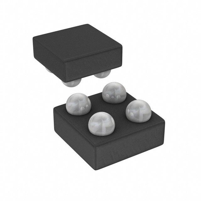
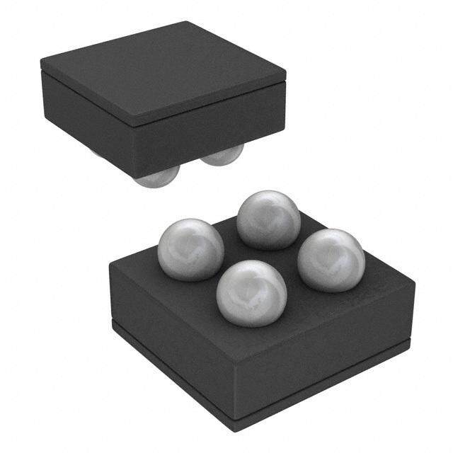
| 描述 | IC DETECTOR RF/IF TRUPWR 4-WLCSP |
| 产品分类 | |
| 品牌 | Analog Devices Inc |
| 数据手册 | |
| 产品图片 |
|
| 产品型号 | ADL5500ACBZ-P7 |
| PCN封装 | |
| RF类型 | 手机,CDMA2000,W-CDMA |
| rohs | 无铅 / 符合限制有害物质指令(RoHS)规范要求 |
| 产品系列 | - |
| 产品目录页面 | |
| 其它名称 | ADL5500ACBZ-P7DKR |
| 包装 | Digi-Reel® |
| 封装/外壳 | 4-WFBGA,WLCSP |
| 标准包装 | 1 |
| 电压-电源 | 2.7 V ~ 5.5 V |
| 电流-电源 | 1mA |
| 精度 | ± 0.1dB |
| 视频文件 | http://www.digikey.cn/classic/video.aspx?PlayerID=1364138032001&width=640&height=505&videoID=2245193150001 |
| 输入范围 | -18.5dBm ~ 6dBm |
| 频率 | 100MHz ~ 6GHz |


- 商务部:美国ITC正式对集成电路等产品启动337调查
- 曝三星4nm工艺存在良率问题 高通将骁龙8 Gen1或转产台积电
- 太阳诱电将投资9.5亿元在常州建新厂生产MLCC 预计2023年完工
- 英特尔发布欧洲新工厂建设计划 深化IDM 2.0 战略
- 台积电先进制程称霸业界 有大客户加持明年业绩稳了
- 达到5530亿美元!SIA预计今年全球半导体销售额将创下新高
- 英特尔拟将自动驾驶子公司Mobileye上市 估值或超500亿美元
- 三星加码芯片和SET,合并消费电子和移动部门,撤换高东真等 CEO
- 三星电子宣布重大人事变动 还合并消费电子和移动部门
- 海关总署:前11个月进口集成电路产品价值2.52万亿元 增长14.8%


PDF Datasheet 数据手册内容提取
100 MHz to 6 GHz TruPwr Detector Data Sheet ADL5500 FEATURES The ADL5500 offers excellent temperature stability with near 0 dB measurement error across temperature. The high accuracy True rms response range, centered around +3 dBm at 900 MHz, offers ±0.1 dB Excellent temperature stability error from −40°C to +85°C over an 8.5 dB range. The ADL5500 ±0.1 dB accuracy vs. temperature over top 8 dB of input range reduces calibration requirements with low drift across a 30 dB Up to 30 dB input dynamic range at 3.9 GHz range over temperature and process variations. 50 Ω input impedance 1250 mV rms, +15 dBm, maximum input The ADL5500 operates from −40°C to +85°C and is available in Single-supply operation: 2.7 V to 5.5 V a 4-ball, 1.0 mm × 1.0 mm wafer-level chip scale package. It is Low power: 3 mW at 3 V supply fabricated on a proprietary high f silicon bipolar process. T RoHS compliant 5 APPLICATIONS Measurement of CDMA2000, W-CDMA, and QPSK-/QAM- based OFDM, and other complex modulation waveforms RF transmitter or receiver power measurement 1 V) GENERAL DESCRIPTION T ( U P T The ADL5500 is a mean-responding power detector for use in OU high frequency receiver and transmitter signal chains from 100 MHz to 6 GHz. It is easy to apply, requiring only a single 0.1 supply between 2.7 V and 5.5 V and a power supply decoupling cinappuact iitmorp. eTdhaen icnep ouft 5is0 iΩnt.e Trnhael olyu atpc-ucto ius pal elidn eaanrd-r hesaps oan ndoinmgi ndacl 0.03 05546-001 –25 –20 –15 –10 –5 0 5 10 15 voltage with a conversion gain of 6.4 V/V rms at 900 MHz. The INPUT (dBm) on-chip, 1 kΩ series resistance at the output combined with an Figure 1. Output vs. Input Level, Supply 3 V, Frequency 1.9 GHz external shunt capacitor creates a low-pass filter response that reduces the residual ripple in the dc output voltage. The ADL5500 is intended for true power measurement of simple and complex waveforms. The device is particularly useful for measuring high crest factor (high peak-to-rms ratio) signals, such as CDMA2000, W-CDMA, and QPSK/QAM-based OFDM waveforms. FUNCTIONAL BLOCK DIAGRAM ADL5500 VPOS INTERNAL FILTER i CAPACITOR RFIN x2 TRANS- CONDUCTANCE CELLS ERROR AMP i x2 BUFFER VRMS 1kΩ COMM 05546-002 Figure 2. Rev. B Document Feedback Information furnished by Analog Devices is believed to be accurate and reliable. However, no responsibility is assumed by Analog Devices for its use, nor for any infringements of patents or other One Technology Way, P.O. Box 9106, Norwood, MA 02062-9106, U.S.A. rights of third parties that may result from its use. Specifications subject to change without notice. No license is granted by implication or otherwise under any patent or patent rights of Analog Devices. Tel: 781.329.4700 ©2005–2015 Analog Devices, Inc. All rights reserved. Trademarks and registered trademarks are the property of their respective owners. Technical Support www.analog.com
ADL5500 Data Sheet TABLE OF CONTENTS Features .............................................................................................. 1 Input Coupling Using a Series Resistor ................................... 16 Applications ....................................................................................... 1 Multiple RF Inputs ..................................................................... 16 General Description ......................................................................... 1 Selecting the Output Low-Pass Filter Network ...................... 16 Functional Block Diagram .............................................................. 1 Power Consumption and Power-On/-Off Response ............. 16 Revision History ............................................................................... 2 Output Drive Capability and Buffering ................................... 17 Specifications ..................................................................................... 3 VRMS Output Offset ................................................................. 17 Absolute Maximum Ratings ............................................................ 7 Device Calibration and Error Calculation .............................. 18 ESD Caution .................................................................................. 7 Calibration for Improved Accuracy ......................................... 18 Pin Configuration and Function Descriptions ............................. 8 Drift over a Reduced Temperature Range .............................. 19 Typical Performance Characteristics ............................................. 9 Operation Above 4.0 GHz ......................................................... 19 Circuit Description ......................................................................... 14 Device Handling ......................................................................... 19 Filtering ........................................................................................ 14 Evaluation Board ........................................................................ 20 Applications Information .............................................................. 15 Outline Dimensions ....................................................................... 22 Basic Connections ...................................................................... 15 Ordering Guide .......................................................................... 22 Output Swing .............................................................................. 15 Linearity ....................................................................................... 15 REVISION HISTORY 12/15—Rev A to Rev. B Changes to Table 2 ............................................................................ 7 Changed Applications Section to Applications Information Section .............................................................................................. 15 Added Junction-to-Board Thermal Impedance Section ........... 20 Change to Figure 53 Caption ........................................................ 22 Changes to Ordering Guide .......................................................... 22 2/06—Rev 0 to Rev. A Changes to Features .......................................................................... 1 Changes to Table 2 ............................................................................ 7 Changes to Figure 5 .......................................................................... 9 Changes to Figure 28 and Figure 31 ............................................. 13 Changes to Figure 35 Caption ....................................................... 15 Changes to Power Consumption and Power-On/-Off Response Section ............................................................................ 16 Changes to Figure 48 ...................................................................... 20 Changes to Ordering Guide .......................................................... 22 7/05—Revision 0: Initial Version Rev. B | Page 2 of 24
Data Sheet ADL5500 SPECIFICATIONS T = 25°C, V = 3.0 V, C = 10 nF, light condition ≤ 600 LUX, unless otherwise noted. A S FLT Table 1. Parameter Test Conditions/Comments Min Typ Max Unit FREQUENCY RANGE Input RFIN 100 6000 MHz RMS CONVERSION (f = 100 MHz) Input RFIN to output VRMS Input Impedance 94||3 Ω||pF Input Return Loss 10 dB Dynamic Range1 CW input, −40°C < T < +85°C A ±0.1 dB Error2 Delta from 25°C, V = 5 V 5 dB S ±0.25 dB Error3 V = 3 V 17.5 dB S V = 5 V 20 dB S ±1 dB Error3 V = 3 V 25 dB S V = 5 V 29 dB S ±2 dB Error3 V = 3 V 28.5 dB S V = 5 V 33 dB S Maximum Input Level ±0.25 dB error3 6 dBm Minimum Input Level ±1 dB error3 −18.5 dBm Conversion Gain VOUT = (Gain × V ) + Intercept 6.1 V/V rms IN V = 5 V 4.6 7.2 V/V rms S Output Intercept4 0.03 V V = 5 V −20 +100 mV S Output Voltage—High Power In P = +5 dBm, 400 mV rms 2.43 V IN Output Voltage—Low Power In P = −21 dBm, 20 mV rms 0.14 V IN Temperature Sensitivity P = −5 dBm IN 25°C ≤ T ≤ 85°C 0.0032 dB/°C A −40°C ≤ T ≤ +25°C −0.0042 dB/°C A RMS CONVERSION (f = 450 MHz) Input RFIN to output VRMS Input Impedance 75||1.4 Ω||pF Input Return Loss 12.5 dB Dynamic Range1 CW input, −40°C < T < +85°C A ±0.1 dB Error2 Delta from 25°C, V = 5 V 8 dB S ±0.25 dB Error3 V = 3 V 19 dB S V = 5 V 24 dB S ±1 dB Error3 V = 3 V 24.5 dB S V = 5 V 29 dB S ±2 dB Error3 V = 3 V 27.5 dB S V = 5 V 33 dB S Maximum Input Level ±0.25 dB error3 5 dBm Minimum Input Level ±1 dB error3 −19.5 dBm Conversion Gain VOUT = (Gain × V ) + Intercept 6.9 V/V rms IN Output Intercept4 0.03 V Output Voltage—High Power In P = +5 dBm, 400 mV rms 2.8 V IN Output Voltage—Low Power In P = −21 dBm, 20 mV rms 0.16 V IN Temperature Sensitivity P = −5 dBm IN 25°C ≤ T ≤ 85°C 0.0020 dB/°C A −40°C ≤T ≤ +25°C −0.0023 dB/°C A Rev. B | Page 3 of 24
ADL5500 Data Sheet Parameter Test Conditions/Comments Min Typ Max Unit RMS CONVERSION (f = 900 MHz) Input RFIN to output VRMS Input Impedance 62||1.1 Ω||pF Input Return Loss 13 dB Dynamic Range1 CW input, −40°C < T < +85°C A ±0.1 dB Error2 Delta from 25°C, V = 5 V 8.5 dB S ±0.25 dB Error3 V = 3 V 19.5 dB S V = 5 V 23 dB S ±1 dB Error3 V = 3 V 24.5 dB S V = 5 V 29 dB S ±2 dB Error3 V = 3 V 28 dB S V = 5 V 32 dB S Maximum Input Level ±0.25 dB error3 6 dBm Minimum Input Level ±1 dB error3 −19 dBm Conversion Gain VOUT = (Gain × V ) + Intercept 6.4 V/V rms IN Output Intercept4 0.04 V Output Voltage—High Power In P = +5 dBm, 400 mV rms 2.61 V IN Output Voltage—Low Power In P = −21 dBm, 20 mV rms 0.15 V IN Temperature Sensitivity P = −5 dBm IN 25°C ≤ T ≤ +85°C 0.0018 dB/°C A −40°C ≤ T ≤ +25°C −0.0023 dB/°C A RMS CONVERSION (f = 1900 MHz) Input RFIN to output VRMS Input Impedance 43||0.9 Ω||pF Input Return Loss 11.5 dB Dynamic Range1 CW input, −40°C < T < +85°C A ±0.1 dB Error2 Delta from 25°C, V = 5 V 7 dB S ±0.25 dB Error3 V = 3 V 20 dB S V = 5 V 23 dB S ±1 dB Error3 V = 3 V 26 dB S V = 5 V 30 dB S ±2 dB Error3 V = 3 V 31.5 dB S V = 5 V 33 dB S Maximum Input Level ±0.25 dB error3 8 dBm Minimum Input Level ±1 dB error3 −19.5 dBm Conversion Gain VOUT = (Gain × V ) + Intercept 5.0 V/V rms IN Output Intercept4 0.02 V Output Voltage—High Power In P = +5 dBm, 400 mV rms 2.02 V IN Output Voltage—Low Power In P = −21 dBm, 20 mV rms 0.11 V IN Temperature Sensitivity P = −5 dBm IN 25°C ≤ T ≤ 85°C 0.0017 dB/°C A −40°C ≤ T ≤ +25°C −0.0031 dB/°C A Rev. B | Page 4 of 24
Data Sheet ADL5500 Parameter Test Conditions/Comments Min Typ Max Unit RMS CONVERSION (f = 2350 MHz) Input RFIN to output VRMS Input Impedance 37||0.9 Ω||pF Input Return Loss 9 dB Dynamic Range1 CW input, −40°C < T < +85°C A ±0.1 dB Error2 Delta from 25°C, V = 5 V 5 dB S ±0.25 dB Error3 V = 3 V 5 dB S V = 5 V 10 dB S ±1 dB Error3 V = 3 V 28.5 dB S V = 5 V 32 dB S ±2 dB Error3 V = 3 V 32 dB S V = 5 V 36 dB S Maximum Input Level ±0.25 dB error3 8 dBm Minimum Input Level ±1 dB error3 −19.5 dBm Conversion Gain VOUT = (Gain × V ) + Intercept 4.5 V/V rms IN Output Intercept4 0.02 V Output Voltage—High Power In P = +5 dBm, 400 mV rms 1.82 V IN Output Voltage—Low Power In P = −21 dBm, 20 mV rms 0.11 V IN Temperature Sensitivity P = −5 dBm IN 25°C ≤ T ≤ 85°C 0.0027 dB/°C A −40°C ≤ T ≤ +25°C −0.0046 dB/°C A RMS CONVERSION (f = 2700 MHz) Input RFIN to output VRMS Input Impedance 34||0.8 Ω||pF Input Return Loss 8.5 dB Dynamic Range1 CW input, −40°C < T < +85°C A ±0.1 dB Error2 Delta from 25°C, V = 5 V 5 dB S ±0.25 dB Error3 V = 3 V 5 dB S V = 5 V 8.5 dB S ±1 dB Error3 V = 3 V 28.5 dB S V = 5 V 32 dB S ±2 dB Error3 V = 3 V 33 dB S V = 5 V 36 dB S Maximum Input Level ±0.25 dB error3 9 dBm Minimum Input Level ±1 dB error3 −19.5 dBm Conversion Gain VOUT = (Gain × V ) + Intercept 4.2 V/V rms IN Output Intercept4 0.02 V Output Voltage—High Power In P =+5 dBm, 400 mV rms 1.67 V IN Output Voltage—Low Power In P = −21 dBm, 20 mV rms 0.1 V IN Temperature Sensitivity P = −5 dBm IN 25°C ≤ T ≤ 85°C 0.0030 dB/°C A −40°C ≤ T ≤ +25°C −0.0049 dB/°C A Rev. B | Page 5 of 24
ADL5500 Data Sheet Parameter Test Conditions/Comments Min Typ Max Unit RMS CONVERSION (f = 3900 MHz) Input RFIN to output VRMS Input Impedance 30||0.6 Ω||pF Input Return Loss 9 dB Dynamic Range1 CW input, −40°C < T < +85°C A ±0.1 dB Error2 Delta from 25°C, V = 5 V 2 dB S ±0.25 dB Error3 V = 3 V 5.5 dB S V = 5 V 8 dB S ±1 dB Error3 V = 3 V 28.5 dB S V = 5 V 32 dB S ±2 dB Error3 V = 3 V 34 dB S V = 5 V 36.5 dB S Maximum Input Level ±0.25 dB error3 12 dBm Minimum Input Level ±1 dB error3 −17 dBm Conversion Gain VOUT = (Gain × V ) + Intercept 3.2 V/V rms IN Output Intercept4 0.02 V Output Voltage—High Power In P = +5 dBm, 400 mV rms 1.28 V IN Output Voltage—Low Power In P = −21 dBm, 20 mV rms 0.08 V IN Temperature Sensitivity P = −5 dBm IN 25°C ≤ T ≤ 85°C 0.0035 dB/°C A −40°C ≤ T ≤ +25°C −0.0066 dB/°C A OUTPUT OFFSET No signal at RFIN 40 150 mV POWER SUPPLIES Operating Range −40°C < T < +85°C 2.7 5.5 V A Quiescent Current No signal at RFIN5 1.0 mA 1 The available output swing, and hence the dynamic range, is altered by the supply voltage; see Figure 8. 2 Error referred to delta from 25°C response; see Figure 16 through Figure 21. 3 Error referred to best-fit line at 25°C 4 Calculated using linear regression. 5 Supply current is input level dependent; see Figure 6. Rev. B | Page 6 of 24
Data Sheet ADL5500 ABSOLUTE MAXIMUM RATINGS Stresses at or above those listed under Absolute Maximum Table 2. Ratings may cause permanent damage to the product. This is a Parameter Rating stress rating only; functional operation of the product at these Supply Voltage V 5.5 V S or any other conditions above those indicated in the operational VRMS 0 V, V S section of this specification is not implied. Operation beyond RFIN 1.25 V rms the maximum operating conditions for extended periods may Equivalent Power, re 50 Ω 15 dBm affect product reliability. Internal Power Dissipation 150 mW θJA (WLCSP) 260°C/W ESD CAUTION θ (WLCSP) 56.3°C/W1 JB Maximum Junction Temperature 125°C Operating Temperature Range −40°C to +85°C Storage Temperature Range −65°C to +150°C 1 See the Junction-to-Board Thermal Impedance section for further details Rev. B | Page 7 of 24
ADL5500 Data Sheet PIN CONFIGURATION AND FUNCTION DESCRIPTIONS BUMP 1 INDICATOR VRMS VPOS 1 4 COMM RFIN 2 3 05546-003 TOP VIEW (BUMP SIDE DOWN) Not to Scale Figure 3. 4-Ball WLCSP Pin Configuration Table 3. Pin Function Descriptions Ball No. Mnemonic Description 1 VRMS Output Pin. Rail-to-rail voltage output with limited current drive capability. The output has an internal 1 kΩ series resistance. High resistive loads are recommended to preserve output swing. 2 COMM Device Ground Pin. 3 RFIN Signal Input Pin. Internally ac-coupled after internal termination resistance. Nominal 50 Ω input impedance. 4 VPOS Supply Voltage Pin. Operational range 2.7 V to 5.5 V. Rev. B | Page 8 of 24
Data Sheet ADL5500 TYPICAL PERFORMANCE CHARACTERISTICS T = 25°C, V = 5.0 V, C = 10 nF, light condition ≤ 600 LUX, Colors: black = +25°C, blue = −40°C, red = +85°C, unless otherwise noted. A S FLT 10 3 100MHz 450MHz 900MHz 2 1900MHz 2350MHz 2700MHz 3900MHz 1 1 V) B) PUT ( OR (d 0 OUT ERR 0.1 100MHz –1 450MHz 900MHz 1900MHz 2350MHz –2 0.03 23790000MMHHzz 05546-004 –3 05546-007 –25 –20 –15 –10 –5 0 5 10 15 –25 –20 –15 –10 –5 0 5 10 15 INPUT (dBm) INPUT (dBm) Figure 4. Output vs. Input Level, Frequencies 100 MHz, 450 MHz, 900 MHz, Figure 7. Linearity Error vs. Input Level, Frequencies 100 MHz, 450 MHz, 1900 MHz, 2350 MHz, 2700 MHz, and 3900 MHz, Supply 5.0 V 900 MHz, 1900 MHz, 2350 MHz, 2700 MHz, and 3900 MHz, Supply 5.0 V 5.0 10 4.5 5.5V 5.0V 4.0 2.7V 3.5 3.0V V) 3.0 V) 1 T ( T ( PU 2.5 PU T T U U O 2.0 O 1.5 100MHz 450MHz 1.0 900MHz 0.1 1900MHz 0.50 223379500000MMMHHHzzz 0.03 05546-008 0 0.2 0.4 IN0P.6UT (V r0m.8s) 1.0 1.2 1.4 05546-005 –25 –20 –15 –10INPUT– 5(dBm)0 5 10 15 Figure 5. Output vs. Input Level (Linear Scale), Frequencies 100 MHz, 450 MHz, Figure 8. Output vs. Input Level, 900 MHz,1900 MHz, 2350 MHz, 2700 MHz, and 3900 MHz, Supply 5.0 V Supply 2.7 V, 3.0 V, 5.0 V, and 5.5 V, Frequency 900 MHz 11 25 10 9 A) 8 3.0V 20 T (m 7 5.0V dB) EN S ( R 6 S R O CU 5 N L 15 PLY 4 TUR P E U R S 3 10 2 01 05546-006 5 05546-009 0 0.1 0.2 0.3 0.4 0.5 0.6 0.7 0.8 0.9 0 1 2 3 4 5 6 INPUT (V rms) FREQUENCY (GHz) Figure 6. Supply Current vs. Input Level, Supplies 3.0 V and 5.0 V, Figure 9. Return Loss vs. Frequency Temperatures −40°C, +25°C, and +85°C Rev. B | Page 9 of 24
ADL5500 Data Sheet 3 3 2 2 1 1 B) B) d d OR ( 0 OR ( 0 R R R R E E –1 –1 –2 –2 –3 05546-010 –3 05546-013 –25 –20 –15 –10 –5 0 5 10 15 –25 –20 –15 –10 –5 0 5 10 15 INPUT (dBm) INPUT (dBm) Figure 10. Temperature Drift Distributions for 55 Devices at −40°C, +25°C, Figure 13. Temperature Drift Distributions for 55 Devices at −40°C, +25°C, and +85°C vs. +25°C Linear Reference, Frequency 450 MHz, Supply 5.0 V and +85°C vs. +25°C Linear Reference, Frequency 2350 MHz, Supply 5.0 V 3 3 2 2 1 1 B) B) d d OR ( 0 OR ( 0 R R R R E E –1 –1 –2 –2 –3 05546-011 –3 05546-014 –25 –20 –15 –10 –5 0 5 10 15 –25 –20 –15 –10 –5 0 5 10 15 INPUT (dBm) INPUT (dBm) Figure 11. Temperature Drift Distributions for 55 Devices at −40°C, +25°C, Figure 14. Temperature Drift Distributions for 55 Devices at −40°C, +25°C, and +85°C vs. +25°C Linear Reference, Frequency 900 MHz, Supply 5.0 V and +85°C vs. +25°C Linear Reference, Frequency 2700 MHz, Supply 5.0 V 3 3 2 2 1 1 B) B) d d OR ( 0 OR ( 0 R R R R E E –1 –1 –2 –2 –3 05546-012 –3 05546-015 –25 –20 –15 –10 –5 0 5 10 15 –25 –20 –15 –10 –5 0 5 10 15 INPUT (dBm) INPUT (dBm) Figure 12. Temperature Drift Distributions for 55 Devices at −40°C, +25°C, Figure 15. Temperature Drift Distributions for 55 Devices at −40°C, +25°C, and +85°C vs. +25°C Linear Reference, Frequency 1900 MHz, Supply 5.0 V and +85°C vs. +25°C Linear Reference, Frequency 3900 MHz, Supply 5.0 V Rev. B | Page 10 of 24
Data Sheet ADL5500 3 3 2 2 1 1 B) B) d d OR ( 0 OR ( 0 R R R R E E –1 –1 –2 –2 –3 05546-016 –3 05546-019 –25 –20 –15 –10 –5 0 5 10 15 –25 –20 –15 –10 –5 0 5 10 15 INPUT (dBm) INPUT (dBm) Figure 16. Output Delta from +25°C Output Voltage for 55 Devices Figure 19. Output Delta from +25°C Output Voltage for 55 Devices at −40°C and +85°C, Frequency 450 MHz, Supply 5.0 V at −40°C and +85°C, Frequency 2350 MHz, Supply 5.0 V 3 3 2 2 1 1 B) B) d d OR ( 0 OR ( 0 R R R R E E –1 –1 –2 –2 –3 05546-017 –3 05546-020 –25 –20 –15 –10 –5 0 5 10 15 –25 –20 –15 –10 –5 0 5 10 15 INPUT (dBm) INPUT (dBm) Figure 17. Output Delta from +25°C Output Voltage for 55 Devices Figure 20. Output Delta from +25°C Output Voltage for 55 Devices at −40°C and +85°C, Frequency 900 MHz, Supply 5.0 V at −40°C and +85°C, Frequency 2700 MHz, Supply 5.0 V 3 3 2 2 1 1 B) B) d d OR ( 0 OR ( 0 R R R R E E –1 –1 –2 –2 –3 05546-018 –3 05546-021 –25 –20 –15 –10 –5 0 5 10 15 –25 –20 –15 –10 –5 0 5 10 15 INPUT (dBm) INPUT (dBm) Figure 18. Output Delta from +25°C Output Voltage for 55 Devices Figure 21. Output Delta from +25°C Output Voltage for 55 Devices at −40°C and +85°C, Frequency 1900 MHz, Supply 5.0 V at −40°C and +85°C, Frequency 3900 MHz, Supply 5.0 V Rev. B | Page 11 of 24
ADL5500 Data Sheet 10 3.0 CW CW QPSK, 4.8dB CF 2.5 QPSK, 4.8dB CF 8PSK, 4.8dB CF 8PSK, 4.8dB CF 16QAM, 6.3dB CF 2.0 16QAM, 6.3dB CF 64QAM, 7.4dB CF 1.5 64QAM, 7.4dB CF 1 1.0 PUT (V) OR (dB) 0.50 T R OU ER –0.5 0.1 –1.0 –1.5 –2.0 0.03 05546-022 ––23..50 05546-025 –25 –20 –15 –10 –5 0 5 10 15 –25 –20 –15 –10 –5 0 5 10 INPUT (dBm) INPUT (dBm) Figure 22. Output vs. Input Level with Different Waveforms, 10 MHz Signal Figure 25. Error from CW Linear Reference vs. Input with Different Waveforms, BW for All Modulated Signals, Supply 5.0 V, Frequency 1900 MHz 10 MHz Signal BW for All Modulated Signals, Supply 5.0 V, Frequency 1900 MHz 3.0 3.0 CW CW 2.5 BPSK, 11dB CF 2.5 BPSK, 11dB CF QPSK, 11dB CF QPSK, 11dB CF 2.0 16QAM, 12dB CF 2.0 16QAM, 12dB CF 64QAM, 11dB CF 64QAM, 11dB CF 1.5 1.5 1.0 1.0 dB) 0.5 dB) 0.5 OR ( 0 OR ( 0 R R R –0.5 R –0.5 E E –1.0 –1.0 –1.5 –1.5 –2.0 –2.0 ––23..50 05546-023 ––23..50 05546-026 –25 –20 –15 –10 –5 0 5 10 –25 –20 –15 –10 –5 0 5 10 INPUT (dBm) INPUT (dBm) Figure 23. Error from CW Linear Reference vs. Input Level for Various Figure 26. Error from CW Linear Reference vs. Input Level for Various 802.16 OFDM Waveforms at 2.35 GHz, 10 MHz Signal BW and 802.16 OFDM Waveforms at 3.5 GHz, 10 MHz Signal BW and 256 Subcarriers for All Modulated Signals, Supply 5.0 V 256 Subcarriers for All Modulated Signals, Supply 5.0 V 3.0 3.0 CW 12.2kbps, DPCCH (–5.46dB, 15ksps) + DPDCH (0dB, 60ksps), 3.4dB CF 2.0 64kbps, DPCCH (–9.54dB, 15ksps) + 2.0 DPDCH (0dB, 240ksps), 3.4dB CF 144kbps, DPCCH (–11.48dB, 15ksps) + DPDCH (0dB, 480ksps), 3.3dB CF 1.0 384kbps, DPCCH (–11.48dB, 15ksps) + 1.0 DPDCH (0dB, 960ksps), 3.3dB CF B) 768kbps, DPCCH (–11.48dB, 15ksps) + B) OR (d 0 DPDCH1 + 2 (0dB, 960ksps), 5.8dB CF OR (d 0 R R R R E E CW –1.0 –1.0 PICH, 4.7dB CF PICH + FCH (9.6kbps), 4.8dB CF PICH + FCH (9.6kbps) + DCCH, 6.3dB CF –2.0 –2.0 PICH + FCH (9.6kbps) + –3.0 05546-024 –3.0 SPDCICCHCH H( +1 + 5F 3SC.6CHkH b( 9p(1.s65)k3,b .66p.k7sbd) pB+s C),F 7.6dB CF 05546-027 –25 –20 –15 –10 –5 0 5 10 –25 –20 –15 –10 –5 0 5 10 INPUT (dBm) INPUT (dBm) Figure 24. Error from CW Linear Reference vs. Input with Various Figure 27. Error from CW Linear Reference vs. Input with Various WCDMA Up Link Waveforms at 1900 MHz CDMA2000 Reverse Link Waveforms at 900 MHz Rev. B | Page 12 of 24
Data Sheet ADL5500 HP8110A PULSE GENERATOR 50 AD811 HPE3631A POWER SUPPLY 732 ADL5500 ADL5500 FTEETK P PR6O2B04E 1 VRMS VPOS 4 FTEETK P PR6O2B04E 1 VRMS VPOS 4 C4 C2 C1 C4 C2 C1 100pF 0.1F 100pF 0.1F 2 COMM RFIN 3 2 COMM RFIN 3 TEKS CTDOSP7E84C GEHSNPIEG8R6N4AA8TLBOR 05546-028 TEKS CTDOSP7E84C GEHSNPIEG8R6N4AA8TLBOR 05546-031 Figure 28. Hardware Configuration for Output Figure 31. Hardware Configuration for Output Response to Response to Modulated Pulse Input Power Supply Gating Measurements 900MHz PULSED RFIN VPOS 400mV rms 400mV rms RF INPUT RF INPUT 250mV rms 250mV rms 160mV rms 160mV rms VRMS VRMS 500mV PER 70mV rms 500mV PER 70mV rms VERTICAL VERTICAL DIVISION DIVISION 4HD0OIV0RISIsZI OPONENRTAL 05546-029 2HD0OIV0RISIsZI OPONENRTAL 05546-032 Figure 29. Output Response to Modulated Pulse Input for Various RF Input Figure 32. Output Response to Gating on Power Supply for Various RF Input Levels, Supply 3 V, Modulation Frequency 900 MHz, No Filter Capacitor Levels, Supply 3 V, Modulation Frequency 900 MHz, 0.01 μF Filter Capacitor 900MHz PULSED RFIN 400mV rms RF INPUT 250mV rms VRMS 160mV rms 500mV PER VERTICAL DIVISION 70mV rms 400s PER HDOIVRISIZIOONNTAL 05546-030 Figure 30. Output Response to Modulated Pulse Input for Various RF Input Levels, Supply 3 V, Modulation Frequency 900 MHz, 0.01 μF Filter Capacitor Rev. B | Page 13 of 24
ADL5500 Data Sheet CIRCUIT DESCRIPTION The ADL5500 is an rms-responding (mean power) detector that The squaring cells have very wide bandwidth with an intrinsic provides an approach to the exact measurement of RF power that response from dc to microwave. However, the dynamic range of is independent of waveform. It achieves this function by using a such a system is small due in part to the much larger dynamic proprietary technique in which the outputs of two identical range at the output of the squaring cells. There are practical squaring cells are balanced by the action of a high-gain error limitations to the accuracy of sensing very small error signals at amplifier. the bottom end of the dynamic range, arising from small random offsets that limit the attainable accuracy at small inputs. The signal to be measured is applied to the input of the first squaring cell through the input matching network. The input is On the other hand, the squaring cells in the ADL5500 have a matched to offer a broadband 50 Ω input impedance from Class-AB aspect; the peak input is not limited by its quiescent 100 MHz to 6 GHz. The input matching network has a high-pass bias condition but is determined mainly by the eventual loss of corner frequency of approximately 90 MHz. square-law conformance. Consequently, the top end of their response range occurs at a large input level (approximately The ADL5500 responds to the voltage, V , at its input by IN 700 mV rms) while preserving a reasonably accurate square-law squaring this voltage to generate a current proportional to V 2. IN response. The maximum usable range is, in practice, limited by This current is applied to an internal load resistor in parallel the output swing. The rail-to-rail output stage can swing from a with a capacitor, followed by a low-pass filter, which extracts the few millivolts above ground to within 100 mV below the supply. mean of V 2. Although essentially voltage responding, the IN An example of the output induced limit, given a conversion gain associated input impedance calibrates this port in terms of of 6.4 V/V rms at 900 MHz and assuming a maximum output of equivalent power. Therefore, 1 mW corresponds to a voltage 2.9 V with a 3 V supply, has a maximum input of 2.9 V rms/6.4 input of 224 mV rms referenced to 50 Ω. Because both the or 450 mV rms. squaring cell input impedance and the input matching network are frequency dependent, the conversion gain is a function of FILTERING signal frequency. An important aspect of rms-dc conversion is the need for averaging (the function is root-mean-square). The on-chip The voltage across the low-pass filter, whose frequency can be averaging in the square domain has a corner frequency of arbitrarily low, is applied to one input of an error-sensing approximately 150 kHz and is sufficient for common amplifier. A second identical voltage-squaring cell is used to modulation signals, such as CDMA, WCDMA, and QPSK- close a negative feedback loop around this error amplifier. This /QAM-based OFDM (for example, WLAN and WiMAX). It second cell is driven by a fraction of the quasi-dc output voltage ensures the accuracy of rms measurement for these signals; of the ADL5500. When the voltage at the input of the second however, it leaves significant ripple on the output. To reduce squaring cell is equal to the rms value of V , the loop is in a IN this ripple, an external shunt capacitor can be used at the output stable state, and the output then represents the rms value of the to form a low-pass filter with the on-chip 1 kΩ resistance (see input. the Selecting the Output Low-Pass Filter Network section). By completing the feedback path through a second squaring cell, identical to the one receiving the signal to be measured, several benefits arise. First, scaling effects in these cells cancel; therefore, the overall calibration can be accurate, even though the open-loop response of the squaring cells taken separately need not be. Note that in implementing rms-dc conversion, no reference voltage enters into the closed-loop scaling. Second, the tracking in the responses of the dual cells remains very close over temperature, leading to excellent stability of calibration. Rev. B | Page 14 of 24
Data Sheet ADL5500 APPLICATIONS INFORMATION BASIC CONNECTIONS LINEARITY Figure 33 shows the basic connections for the ADL5500. The Because the ADL5500 is a linear-responding device, plots of device is powered by a single supply of between 2.7 V and 5.5 V output voltage vs. input voltage result in a straight line. It is with a quiescent current of 1.0 mA. The VPOS pin is decoupled more useful to plot the error on a logarithmic scale, as shown in using 100 pF and 0.1 µF capacitors. Figure 35. The deviation of the plot for the ideal straight-line characteristic is caused by output clipping at the high end and The ADL5500 RF input does not require external termination by signal offsets at the low end. However, it should be noted that components because it is internally matched for an overall offsets at the low end can be either positive or negative; therefore, broadband input impedance of 50 Ω. this plot could also trend upwards at the low end. Figure 10 +VS2.7V TO 5.5V through Figure 15 show error distributions for a large population of devices. 100pF 0.1µF ADL5500 3 100MHz VRMS 1 VRMS VPOS 4 450MHz CFLT 900MHz 2 1900MHz 2350MHz 2 COMM RFIN 3 RFIN 05546-033 1 23790000MMHHzz Figure 33. Basic Connections for ADL5500 B) d OUTPUT SWING OR ( 0 R R E At 900 MHz, the output voltage is nominally 6.4 times the input –1 rms voltage (a conversion gain of 6.4 V/V rms). The output voltage swings from near ground to 4.9 V on a 5.0 V supply. –2 Finigpuurt ef o3r4 vsahroiowuss t shuep opulytp vuotl tsawgiensg. Iot fi st hcele AarD fLro5m50 F0i tgou rae C 3W4 t hat –3 05546-007 –25 –20 –15 –10 –5 0 5 10 15 operating the device at lower supply voltages reduces dynamic range as the output headroom decreases. INPUT (dBm) Figure 35. Representative Unit, Error in dB vs. Input Level, VS = 5.0 V 10 5.5V It is also apparent in Figure 35 that the error plot tends to shift 5.0V to the right with increasing frequency. The squaring cell has an input impedance that decreases with frequency. The matching 2.7V network compensates for the change and maintains the input 3.0V impedance at a nominal 50 Ω. The result is a decrease in the V) 1 T ( actual voltage across the squaring cell as the frequency increases, U P reducing the conversion gain. Similarly, conversion gain is less T U O at frequencies near 100 MHz because of the small on-chip coupling capacitor. 0.1 0.03 05546-008 –25 –20 –15 –10 –5 0 5 10 15 INPUT (dBm) Figure 34. Output Swing for Supply Voltages of 2.7 V, 3.0 V, 5.0 V, and 5.5 V Rev. B | Page 15 of 24
ADL5500 Data Sheet INPUT COUPLING USING A SERIES RESISTOR The output of the ADL5500 can be filtered by placing a capacitor between VRMS (Pin 1) and ground. The combination of the Figure 36 shows a technique for coupling the input signal into on-chip 1 kΩ output series resistance and the external shunt the ADL5500 that can be applicable where the input signal is capacitor forms a low-pass filter to reduce the residual ac. much larger than the input range of the ADL5500. A series resistor combines with the input impedance of the ADL5500 to Table 4 shows the effect of several capacitor values for various attenuate the input signal. Because this series resistor forms a communications standards with high peak-to-average ratios divider with the frequency dependent input impedance, the along with the residual ripple at the output, in peak-to-peak and apparent gain changes greatly with frequency. However, this rms volts. Note that large load capacitances increase the turn-on method has the advantage of very little power being tapped off and pulse response times (see Figure 29 and Figure 30). in RF power transmission applications. If the resistor is large compared to the transmission line’s impedance, the VSWR of Table 4. Waveform and Output Filter Effects on Residual AC the system is relatively unaffected. Output Residual AC Waveform C V dc mV p-p mV rms FILT 64QAM 0.01 µF 0.5 7.0 1.4 RSERIES RFIN RFIN (7.4 dB CF) 1.0 7.4 1.5 ADL5500 05546-036 0.1 µF 20..05 76..67 11..64 1.0 7.2 1.5 Figure 36. Attenuating the Input Signal 2.0 7.4 1.5 MULTIPLE RF INPUTS W-CDMA RL 0.01 µF 0.5 10 1.7 (3.4 dB CF) 1.0 16 2.4 Figure 37 shows a technique for combining multiple RF input 2.0 45 5.6 signals to the ADL5500. Some applications can share a single 0.1 µF 0.5 7 1.5 detector for multiple bands. Three 16.5 Ω resistors in a T-network 1.0 9 1.6 combine the three 50 Ω terminations (including the ADL5500). 2.0 14 2.3 The broadband resistive combiner ensures each port of the CDMA2000 UL 0.01 µF 0.5 46 6 T-network sees a 50 Ω termination. Because there is only 6 dB (6.7 dB CF) 1.0 85 13 of isolation from one port of the combiner to the other ports, 2.0 191 27 only one band should be active at a time. 0.1 µF 0.5 17 3 BAND1 1.0 31 5 2.0 68 9 DIRECTIONAL COUPLER 50Ω POWER CONSUMPTION AND POWER-ON/-OFF RESPONSE The quiescent current consumption of the ADL5500 varies with 16.5Ω BAND2 the size of the input signal from approximately 1 mA for no 16.5Ω DIRECTIONAL RFIN signal up to 6 mA at an input level of 0.7 V rms (10 dBm, re COUPLER 50Ω 50 Ω). If the input is driven beyond this point, the supply 16.5Ω ADL5500 05546-051 vcuarriraetniot nin icnr eqausieess csehnatr pcluyr (raesn ts hwoiwthn p ionw Feirg usurep p6l)y. Tvohletraeg eis. little Figure 37. Combining Multiple RF Input Signals The ADL5500 can be disabled by simply removing the power to SELECTING THE OUTPUT LOW-PASS FILTER the device. Figure 32 shows a plot of the output response to the NETWORK supply being turned on (that is, VPOS is pulsed) with an output shunt capacitor of 0.01 µF. Again, the turn-on time is influenced The internal filter capacitor of the ADL5500 provides averaging strongly by the size of the output shunt capacitor. in the square domain but leaves some residual ac on the output. Signals with high peak-to-average ratios, such as W-CDMA To improve the falling edge of the supply gating response and or CDMA2000, can produce ac-residual levels on the ADL5500 the pulse response, a resistor can be placed in parallel with the dc output. To reduce the effects of these low frequency output shunt capacitor. The added resistance helps discharge components in the waveforms, some additional filtering is the capacitor. Although this method reduces the power-off time, required. the added load resistor also attenuates the output (see the Output Drive Capability and Buffering section). Rev. B | Page 16 of 24
Data Sheet ADL5500 OUTPUT DRIVE CAPABILITY AND BUFFERING VRMS OUTPUT OFFSET The ADL5500 is capable of sourcing an output current of The ADL5500 has a ±1 dB error detection range of about 30 dB, approximately 3 mA. The output current is sourced through the as shown in Figure 10 to Figure 15. The error is referred to the on-chip 1 kΩ series resistor; therefore, any load resistor forms a best fit line defined in the linear region of the output response. voltage divider with this on-chip resistance. It is recommended Below an input power of −20 dBm, the response is no longer that the ADL5500 drive high resistive loads to preserve output linear and begins to lose accuracy. In addition, depending on swing (preferably >100 kΩ). If an application requires driving the supply voltage, saturation of the output limits the detection a low resistance load, a simple buffering circuit can be used, accuracy above 10 dBm. Choose calibration points in the linear as shown in Figure 40. Similar circuits can be used to increase region, avoiding the nonlinear ranges at the high and low or decrease the nominal conversion gain (see Figure 38 and extremes. Figure 39). In Figure 39, the AD8031 buffers a resistive divider 10 to give half of the slope. In Figure 38, the op amp gain of two doubles the slope. Using other resistor values, the slope can be changed to an arbitrary value. The AD8031 rail-to-rail op amp, used in these examples, can swing from 50 mV to 4.95 V on a single 5 V supply and operates at supply voltages down to 2.7 V. 1 If high output current is required (>10 mA), the AD8051, which T (V) also has rail-to- rail capability, can be used down to a supply U P T voltage of 3 V. It can deliver up to 45 mA of output current. U O 5V 0.1 0.1µF 100pF VPOSVRMS 0.01µF 0.01 05546-040 AD8031 12.8V/V rms –40 –35 –30 –25 –20 –15 –10 –5 0 5 10 ADL5500 INPUT (dBm) Figure 41. Output vs. Input Level Distribution of 55 Devices, COMM Frequency 900 MHz, Supply 3.0 V 5kΩ 5kΩ 05546-037 Fthigeu inrep 4u1t pshoowwers ftohre mdiustltriipbluet dioenv iocfe st.h Te hoeu tApDutL r5e5s0p0o nlossee vss . Figure 38. Output Buffering Options, Slope of 12.8 V/V rms at 900 MHz accuracy at low input powers as the output response begins to 5V fan out. As the input power is reduced, the spread of the output 0.1µF 100pF response increases along with the error. Although some devices follow the ideal linear response at very low input powers, not VPOS all devices continue the ideal linear regression to a near 0 V VRMS 0.01µF y-intercept. Some devices exhibit output responses that rapidly 4kΩ ADL5500 decrease and some flatten out. With no RF signal applied, 5kΩ AD8031 3.2V/V rms the ADL5500 has a typical output offset of 40 mV (with a COMM 05546-038 m aximum of 150 mV). Figure 39. Output Buffering Options, Slope of 3.2 V/V rms at 900 MHz 5V 0.1µF 100pF 0.01µF VPOS VRMS AD8031 6.4V/V rms ADL5500 COMM 05546-039 Figure 40. Output Buffering Options, Slope of 6.4 V/V rms at 900 MHz Rev. B | Page 17 of 24
ADL5500 Data Sheet DEVICE CALIBRATION AND ERROR CALCULATION Figure 42 also includes error plots for the output voltage at −40°C and +85°C. These error plots are calculated using the Because slope and intercept vary from device to device, board- slope and intercept at +25°C. This is consistent with calibration level calibration must be performed to achieve high accuracy. In in a mass-production environment where calibration at general, calibration is performed by applying two input power temperature is not practical. levels to the ADL5500 and measuring the corresponding output voltages. The calibration points are generally chosen to be CALIBRATION FOR IMPROVED ACCURACY within the linear operating range of the device. The best fit line Another way of presenting the error function of the ADL5500 is is characterized by calculating the slope and intercept using the shown in Figure 43. In this case, the dB error at hot and cold following equations: temperatures is calculated with respect to the transfer function Slope = (V − V )/(V − V ) (1) at ambient. This is a key difference in comparison to the RMS2 RMS1 IN2 IN1 previous plots. Up to now, the errors have been calculated with Intercept = V − (Slope × V ) (2) RMS1 IN1 respect to the ideal linear transfer function at ambient. When where: this alternative technique is used, the error at ambient becomes equal to 0 by definition (see Figure 43). V is the rms input voltage to RFIN. IN VRMS is the voltage output at VRMS. This plot is a useful tool for estimating temperature drift at a particular power level with respect to the (nonideal) response at Once slope and intercept have been calculated, an equation can ambient. The linearity and dynamic range tend to be improved be written that allows calculation of an (unknown) input power artificially with this type of plot because the ADL5500 does not based on the measured output voltage. perfectly follow the ideal linear equation (especially outside of VIN = (VRMS − Intercept)/Slope (3) its linear operating range). Achieving this level of accuracy in an end application requires calibration at multiple points in the For an ideal (known) input power, the law conformance error of operating range of the device. the measured data can be calculated as In some applications, very high accuracy is required at just one ERROR (dB) = power level or over a reduced input range. For example, in a 20 × log [(V − Intercept)/(Slope × V )] (4) RMS, MEASURED IN, IDEAL wireless transmitter, the accuracy of the high power amplifier Figure 42 includes a plot of the error at 25°C, the temperature at (HPA) is most critical at or close to full power. The ADL5500 which the ADL5500 is calibrated. Note that the error is not zero. offers a tight error distribution in the high input power range, This is because the ADL5500 does not perfectly follow the ideal as shown in Figure 43. The high accuracy range, centered linear equation, even within its operating region. The error at around +3 dBm at 900 MHz, offers 8.5 dB of ±0.1 dB detection the calibration points is, however, equal to zero by definition. error over temperature. Multiple point calibration at ambient temperature in the reduced range offers precise power 3 measurement with near 0 dB error from −40°C to +85°C. 2 3 1 2 +85°C B) +25°C d OR ( 0 1 ERR –1 –40°C OR (dB) 0 +85°C +25°C R R E –40°C –2 –1 –3 05546-052 –2 –25 –20 –15 –10INPUT– 5(dBm)0 5 10 15 –3 05546-053 Figure 42. Error from Linear Reference vs. Input at −40°C, +25°C, and +85°C –25 –20 –15 –10 –5 0 5 10 15 vs. +25°C Linear Reference, Frequency 900 MHz, Supply 5.0 V INPUT (dBm) Figure 43. Error from +25°C Output Voltage at −40°C, +25°C, and +85°C After Ambient Normalization, Frequency 900 MHz, Supply 5.0 V Rev. B | Page 18 of 24
Data Sheet ADL5500 The high accuracy range center varies over frequency. At 3 900 MHz, the region is centered at approximately 3 dBm. At higher frequencies, the high accuracy range is centered at 2 higher input powers (see Figure 16 to Figure 21). DRIFT OVER A REDUCED TEMPERATURE RANGE 1 B) d Figure 44 shows the error over temperature for a 1.9 GHz input OR ( 0 signal. Error due to drift over temperature consistently remains R R within ±0.25 dB and only begins to exceed this limit when the E –1 ambient temperature goes above +50°C and below −10°C. For all frequencies using a reduced temperature range, higher measurement accuracy is achievable. –2 1.00 +85°C –3 05546-042 +70°C –25 –20 –15 –10 –5 0 5 10 15 0.75 +50°C +30°C INPUT (dBm) +25°C 0.50 +15°C Figure 45. Temperature Drift Distributions for Six Devices at −40°C, +25°C, 0°C and +85°C After Ambient Normalization, Frequency 5.0 GHz, Supply 5.0 V –10°C B) 0.25 ––2450°°CC 3 d OR ( 0 R R 2 E –0.25 –0.50 1 B) d ––01..7050 05546-041 ERROR ( 0 –20 –15 –10 –5 0 5 10 15 –1 INPUT (dBm) Figure 44. Typical Drift at 1.9 GHz for Various Temperatures –2 OThPeE ARDALT5I5O00N w AorBkOs aVt Efr e4q.u0e nGcHiezs above 4.0 GHz, but exhibits –3 05546-043 –25 –20 –15 –10 –5 0 5 10 15 slightly higher output voltage temperature drift. Figure 45 and INPUT (dBm) Figure 46 show the error distributions of six devices at 5.0 GHz Figure 46. Temperature Drift Distributions for Six Devices at −40°C, +25°C, and 6.0 GHz over temperature. Although the temperature drift and +85°C After Ambient Normalization, Frequency 6.0 GHz, Supply 5.0 V is larger than at lower frequencies, the error distributions at DEVICE HANDLING each temperature remain tight throughout the central linear region. Due to the repeatability of the drift from device-to- The wafer-level chip scale package consists of solder bumps device, compensation can be applied to reduce the effects of connected to the active side of the die. The device is lead-free temperature drift. with 95.5% tin, 4.0% silver, and 0.5% copper solder bump composition. The WLCSP can be mounted on printed circuit boards using standard surface-mount assembly techniques; however, take caution to avoid damaging the die. See the AN-617 Application Note for additional information. WLCSP devices are bumped die; therefore, the exposed die can be sensitive to light, which can influence specified limits. Lighting in excess of 600 LUX can degrade performance. Rev. B | Page 19 of 24
ADL5500 Data Sheet EVALUATION BOARD 0.30 mm (50Ω) Figure 48 shows the schematic of the ADL5500 evaluation board. The layout and silkscreen of the evaluation board layers 0.20 mm 0.28 mm are shown in Figure 49 to Figure 52. The board is powered by a 0.15 mm single supply in the 2.7 V to 5.5 V range. The power supply is decoupled by 100 pF and 0.01 µF capacitors. Table 5 details the VPOS RFIN various configuration options of the evaluation board. 0.50 mm Problems caused by impedance mismatch can arise using the 0.50 mm evaluation board to examine the ADL5500 performance. One way to reduce these problems is to put a coaxial 3 dB attenuator on the RFIN SMA connector. Mismatches at the source, cable, (PASTE MASK0 O.3P8E mNmING) VRMS COMM and cable interconnection, as well as those occurring on the GROUND evaluation board, can cause these problems. 0.15 mm PLANE A simple (and common) example of such a problem is triple travel due to mismatch at both the source and the evaluation board. Here the signal from the source reaches the evaluation 05546-054 board and mismatch causes a reflection. When that reflection Figure 47. Land Pattern Used on the ADL5500 Evaluation Board reaches the source mismatch, it causes a new reflection, which travels back to the evaluation board, adding to the original Junction-to-Board Thermal Impedance signal incident at the board. The resultant voltage varies with The junction-to-board thermal impedance (θ ) is the thermal JB both cable length and frequency dependence on the relative impedance from the die to the bottom plane of the four balls of the phase of the initial and reflected signals. Placing the 3 dB pad at ADL5500. For the ADL5500, θ was determined experimentally to JB the input of the board improves the match at the board and thus be 56.3°C/W with the device mounted on a 4-layer circuit board reduces the sensitivity to mismatches at the source. When such and two layers being ground planes in a configuration similar to precautions are taken, measurements are less sensitive to cable that of the ADL5500-EVALZ evaluation board. Board size and length and other fixture issues. In an actual application when complexity (number of layers) affect θ ; more layers tend to JB the distance between ADL5500 and source is short and well- reduce thermal impedance slightly. defined, this 3 dB attenuator is not needed. If the board temperature is known, use the junction-to-board Land Pattern and Soldering Information thermal impedance to calculate the die temperature (also known Figure 47 shows the land pattern used on the ADL5500 as junction temperature) to ensure that it does not exceed the evaluation board. Pad diameters of 0.28 mm are used with a specified limit of 125°C. For example, if the board temperature solder paste mask opening of 0.38 mm. For the RF input trace, a is 85°C, the die temperature is given by the equation trace width of 0.30 mm is used, which corresponds to a 50 Ω T = T + (P × θ ) J B DISS JB characteristic impedance for the dielectric material being used (FR4). All traces going to the pads are tapered down to 0.15 mm. The worst case power dissipation for the ADL5500 is 58 mW For the RFIN line, the length of the tapered section is 0.20 mm. (5.5 V × 10.5 mA, see Figure 6). Therefore, TJ is T = 85°C + (0.058 W × 56.3°C/W) = 88.26°C J TO EDGE CONNECTOR R6 (OPEN) C1 C2 R3 ADL5500 100pF 0.1µF 0Ω VRMS 1 VRMS VPOS 4 VPOS C4 R8 10nF (OPEN) 2 COMM RFIN 3 RFIN 05546-044 Figure 48. Evaluation Board Schematic Rev. B | Page 20 of 24
Data Sheet ADL5500 Table 5. Evaluation Board Configuration Options Component Description Default Condition VPOS, GND Ground and Supply Vector Pins. Not Applicable C1, C2 Power Supply Decoupling. The nominal supply decoupling of 0.01 µF and 100 pF. C1 = 0.01 µF (Size 0402) C2 = 100 pF (Size 0402) R3, R8, C4 Output Filtering. The combination of the internal 1 kΩ output resistance and C4 produce R3 = 0 Ω (Size 0402) a low-pass filter to reduce output ripple. The output can also be scaled down using the R8 = Open (Size 0402) resistor divider pads, R3 and R8. In addition, resistors and capacitors can be placed in C4 and C4 = 10 nF (Size 0402) R8 to load test VRMS. R6 Alternate Interface. R6 allows VOUT to be accessible from the edge connector, which is only R6 = Open (Size 0402) used for characterization. 05546-045 05546-047 Figure 49. Layout of Component Side (WLCSP) Figure 51. Silkscreen of Component Side (WLCSP) 05546-046 05546-048 Figure 50. Layout of Circuit Side (WLCSP) Figure 52. Silkscreen of Circuit Side (WLCSP) Rev. B | Page 21 of 24
ADL5500 Data Sheet OUTLINE DIMENSIONS 0.675 10..091600 SQ 00..338516 00..559166 CAO1 RBNAELRL 0.910 0.331 SPLEAATNIENG 2 1 A 0.345 0.295 0.245 0.50 BSC B BALL PITCH TOP VIEW 0.270 BOTTOM VIEW (BALL SIDE DOWN) 0.240 (BALL SIDE UP) 0.210 0.030 NOM COPLANARITY 111105-0 Figure 53. 4-Ball Wafer-Level Chip Scale Package [WLCSP] (CB-4-1) Dimensions shown in millimeters ORDERING GUIDE Ordering Model1 Temperature Range Package Description Package Option Branding Quantity ADL5500ACBZ-P7 −40°C to +85°C 4-Ball WLCSP, 7” Pocket Tape and Reel CB-4-1 Q06 3,000 ADL5500-EVALZ Evaluation Board 1 Z = RoHS Compliant Part. Rev. B | Page 22 of 24
Data Sheet ADL5500 NOTES Rev. B | Page 23 of 24
ADL5500 Data Sheet NOTES ©2005–2015 Analog Devices, Inc. All rights reserved. Trademarks and registered trademarks are the property of their respective owners. D05546–0–12/15(B) Rev. B | Page 24 of 24