ICGOO在线商城 > 射频/IF 和 RFID > RF 检测器 > AD8314ARM
 Datasheet下载
- 型号: AD8314ARM
- 制造商: Analog
- 库位|库存: xxxx|xxxx
- 要求:
| 数量阶梯 | 香港交货 | 国内含税 |
| +xxxx | $xxxx | ¥xxxx |
查看当月历史价格
查看今年历史价格
AD8314ARM产品简介:
ICGOO电子元器件商城为您提供AD8314ARM由Analog设计生产,在icgoo商城现货销售,并且可以通过原厂、代理商等渠道进行代购。 AD8314ARM价格参考。AnalogAD8314ARM封装/规格:RF 检测器, RF Detector IC Cellular, GSM, TDMA, CDMA 100MHz ~ 2.7GHz -45dBm ~ 0dBm 8-TSSOP, 8-MSOP (0.118", 3.00mm Width)。您可以下载AD8314ARM参考资料、Datasheet数据手册功能说明书,资料中有AD8314ARM 详细功能的应用电路图电压和使用方法及教程。
AD8314ARM是由Analog Devices Inc.(亚德诺半导体公司)生产的一款RF(射频)检测器。它主要用于测量和监控射频信号的功率水平,广泛应用于无线通信、雷达系统、测试设备等领域。以下是AD8314ARM的主要应用场景:

1. 无线通信设备:AD8314ARM可以用于基站、中继站和移动终端等设备中,实时监测射频信号的功率,确保发射功率在规定范围内,避免过载或不足。它还可以帮助优化信号传输质量,减少干扰。

2. 雷达系统:在雷达应用中,AD8314ARM能够精确测量反射回来的射频信号强度,帮助系统判断目标的距离、速度等信息。它还可以用于监控雷达发射机的输出功率,确保系统稳定运行。

3. 测试与测量仪器:在实验室或生产线上的测试设备中,AD8314ARM可以集成到频谱分析仪、信号发生器等设备中,用于测量和校准射频信号的功率。它的高精度和宽动态范围使得它非常适合用于高端测试仪器。

4. 射频识别(RFID)系统:AD8314ARM可以用于RFID读写器中,监测发射和接收信号的功率,确保标签能够被正确识别。它还可以帮助优化系统的功耗和性能。

5. 卫星通信:在卫星通信系统中,AD8314ARM可以用于地面站和卫星之间的信号传输监控,确保信号强度在最佳范围内,从而提高通信质量和可靠性。

6. 医疗设备:一些医疗设备如微波治疗仪、超声波设备等也使用射频技术。AD8314ARM可以用于这些设备中,确保射频能量的安全性和有效性。

7. 物联网(IoT)设备:随着物联网的发展,越来越多的设备需要通过无线网络进行通信。AD8314ARM可以用于这些设备中,确保其射频模块的正常工作,并提供稳定的通信连接。

总之,AD8314ARM凭借其高精度、宽动态范围和低功耗等特点,成为众多射频应用中的理想选择。
| 参数 | 数值 |
| 产品目录 | |
| 描述 | IC RF DETECTOR/CTRLR 45DB 8-MSOP对数放大器 RF Detector/Cntlr 100MHz-2.7GHz 45dB |
| 产品分类 | |
| 品牌 | Analog Devices Inc |
| 产品手册 | |
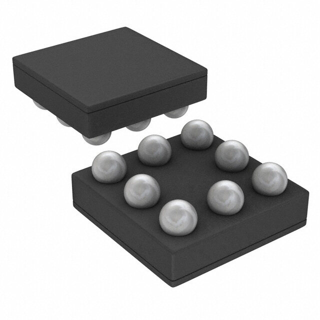
| 产品图片 |
|
| rohs | 否不符合限制有害物质指令(RoHS)规范要求 |
| 产品系列 | 放大器 IC,对数放大器,Analog Devices AD8314ARM- |
| 数据手册 | |
| 产品型号 | AD8314ARM |
| RF类型 | 手机,GSM,TDMA,CDMA |
| 产品 | Logarithmic Amplifiers |
| 产品种类 | 对数放大器 |
| 功率耗散 | 200 mW |
| 包装 | 管件 |
| 商标 | Analog Devices |
| 安装风格 | SMD/SMT |
| 封装 | Tube |
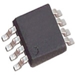
| 封装/外壳 | 8-TSSOP,8-MSOP(0.118",3.00mm 宽) |
| 封装/箱体 | MSOP-8 |
| 工作温度范围 | + 85 C |
| 工作电源电压 | 2.7 V to 5.5 V |
| 工厂包装数量 | 50 |
| 放大器类型 | Logarithmic |
| 最大工作温度 | + 85 C |
| 最小工作温度 | - 40 C |
| 标准包装 | 50 |
| 电压-电源 | 2.7 V ~ 5.5 V |
| 电流-电源 | 5.7mA |
| 电源电流 | 4.5 mA |
| 类型 | Log Amp Detector |
| 精度 | - |
| 系列 | AD8314 |
| 视频文件 | http://www.digikey.cn/classic/video.aspx?PlayerID=1364138032001&width=640&height=505&videoID=2245193150001 |
| 输入电压范围—最大 | 5.5 V |
| 输入范围 | -45dBm ~ 0dBm |
| 通道数量 | 1 Channel |
| 频率 | 100MHz ~ 2.7GHz |


- 商务部:美国ITC正式对集成电路等产品启动337调查
- 曝三星4nm工艺存在良率问题 高通将骁龙8 Gen1或转产台积电
- 太阳诱电将投资9.5亿元在常州建新厂生产MLCC 预计2023年完工
- 英特尔发布欧洲新工厂建设计划 深化IDM 2.0 战略
- 台积电先进制程称霸业界 有大客户加持明年业绩稳了
- 达到5530亿美元!SIA预计今年全球半导体销售额将创下新高
- 英特尔拟将自动驾驶子公司Mobileye上市 估值或超500亿美元
- 三星加码芯片和SET,合并消费电子和移动部门,撤换高东真等 CEO
- 三星电子宣布重大人事变动 还合并消费电子和移动部门
- 海关总署:前11个月进口集成电路产品价值2.52万亿元 增长14.8%


PDF Datasheet 数据手册内容提取
100 MHz to 2.7 GHz, 45 dB RF Detector/Controller Data Sheet AD8314 FEATURES For convenience, the signal is internally ac-coupled, using a 5 pF capacitor to a load of 3 kΩ in shunt with 2 pF. This high- Complete RF detector/controller function pass coupling, with a corner at approximately 16 MHz, Typical range:−58 dBV to −13 dBV determines the lowest operating frequency. Therefore, the −45 dBm to 0 dBm, re 50 Ω source can be dc grounded. Frequency response from 100 MHz to 2.7 GHz Temperature-stable linear-in-dB response The AD8314 provides two voltage outputs. The first, V_UP, Accurate to 2.7 GHz increases from close to ground to about 1.2 V as the input signal Rapid response: 70 ns to a 10 dB step level increases from 1.25 mV to 224 mV. This output is intended Low power: 12 mW at 2.7 V for use in measurement mode. Consult the Applications section Power down to 20 µA for information on this mode. A capacitor can be connected between the V_UP and FLTR pins when it is desirable to APPLICATIONS increase the time interval over which averaging of the input Cellular handsets (TDMA, CDMA , GSM) waveform occurs. RSSI and TSSI for wireless terminal devices The second output, V_DN, is an inversion of V_UP but with Transmitter power measurement and control twice the slope and offset by a fixed amount. This output starts GENERAL DESCRIPTION at about 2.25 V (provided the supply voltage is ≥3.3 V) for the The AD8314 is a complete low cost subsystem for the minimum input and falls to a value close to ground at the measurement and control of RF signals in the frequency range maximum input. This output is intended for analog control of 100 MHz to 2.7 GHz, with a typical dynamic range of 45 dB, loop applications. A setpoint voltage is applied to VSET, and intended for use in a wide variety of cellular handsets and other V_DN is then used to control a VGA or power amplifier. Here wireless devices. It provides a wider dynamic range and better again, an external filter capacitor can be added to extend the accuracy than possible using discrete diode detectors. In averaging time. Consult the Applications section for particular, its temperature stability is excellent over the full information on this mode. operating range of −40°C to +85°C. The AD8314 is available in 8-lead MSOP and 8-lead LFCSP Its high sensitivity allows control at low power levels, thus packages and consumes 4.5 mA from a 2.7 V to 5.5 V supply. reducing the amount of power that needs to be coupled to the When powered down, the typical sleep current is 20 µA. detector. It is essentially a voltage-responding device, with a typical signal range of 1.25 mV to 224 mV rms or –58 dBV to −13 dBV. This is equivalent to −45 dBm to 0 dBm, re 50 Ω. FUNCTIONAL BLOCK DIAGRAM FLTR V-I VSET – + I-V V_UP DET DET DET DET DET – X2 V_DN RFIN + 10dB 10dB 10dB 10dB BAND GAP VPOS OFFSET AD8314 REFERENCE ENBL COMPENSATION (PACDODMLEM) 01086-001 Figure 1. Rev. C Document Feedback Information furnished by Analog Devices is believed to be accurate and reliable. However, no responsibility is assumed by Analog Devices for its use, nor for any infringements of patents or other One Technology Way, P.O. Box 9106, Norwood, MA 02062-9106, U.S.A. rights of third parties that may result from its use. Specifications subject to change without notice. No license is granted by implication or otherwise under any patent or patent rights of Analog Devices. Tel: 781.329.4700 ©2002–2018 Analog Devices, Inc. All rights reserved. Trademarks and registered trademarks are the property of their respective owners. Technical Support www.analog.com
AD8314 Data Sheet TABLE OF CONTENTS Features .............................................................................................. 1 Transfer Function in Terms of Slope and Intercept ............... 12 Applications ....................................................................................... 1 dBV vs. dBm ............................................................................... 13 General Description ......................................................................... 1 Filter Capacitor ........................................................................... 13 Functional Block Diagram .............................................................. 1 Operating in Controller Mode ................................................. 13 Revision History ............................................................................... 2 Power-On and Enable Glitch .................................................... 14 Specifications ..................................................................................... 3 Input Coupling Options ............................................................ 14 Absolute Maximum Ratings ............................................................ 4 Increasing the Logarithmic Slope in Measurement Mode ... 15 ESD Caution .................................................................................. 4 Effect of Waveform Type on Intercept .................................... 15 Pin Configurations and Function Descriptions ........................... 5 Mobile Handset Power Control Examples .............................. 16 Typical Performance Characteristics ............................................. 6 Operation at 2.7 GHz ................................................................. 18 Theory of Operation ...................................................................... 10 Using the LFCSP Package.......................................................... 18 Inverted Output .......................................................................... 11 Evaluation Board ........................................................................ 18 Applications ..................................................................................... 12 Outline Dimensions ....................................................................... 20 Basic Connections ...................................................................... 12 Ordering Guide .......................................................................... 20 REVISION HISTORY 1/2018—Rev. B to Rev. C 3/2002—Rev. 0 to Rev. A Changes to Figure 3 .......................................................................... 5 Edit to Product Description ............................................................. 1 Added EPAD to Table 3 ................................................................... 5 Edit to Specifications ......................................................................... 2 Updated Outline Dimensions ....................................................... 20 Edit to Ordering Guide .................................................................... 3 Changes to Ordering Guide .......................................................... 21 Edit to TPC 1 ...................................................................................... 4 New Section (Operation at 2.7 GHz) Added .............................. 14 5/2006—Rev. A to Rev. B Addition of New Figures 14 and 15 ............................................. 14 Updated Format .................................................................. Universal Changes to Evaluation Board Section.......................................... 14 Changes to General Description .................................................... 1 Addition of Chip Scale Package .................................................... 16 Changes to Table 1 ............................................................................ 3 Changes to Table 2 ............................................................................ 4 10/1999—Revision 0: Initial Version Inserted Figure 3; Renumbered Sequentially ................................ 5 Changes to Figure 4, Figure 5, Figure 6, Figure 7, and Figure 8 ...................................................................................... 6 Changes to Figure 9, Figure 10, and Figure 12 ............................. 7 Changes to Figure 37 ...................................................................... 14 Changes to Table 5 .......................................................................... 15 Changes to Figure 39 ...................................................................... 16 Changes to Table 7 .......................................................................... 19 Updated Outline Dimensions ....................................................... 20 Changes to Ordering Guide .......................................................... 20 Rev. C | Page 2 of 20
Data Sheet AD8314 SPECIFICATIONS V = 3 V, T = 25°C, unless otherwise noted. S A Table 1. Parameter Conditions Min Typ Max Unit OVERALL FUNCTION Frequency Range1 To meet all specifications 0.1 2.5 GHz Input Voltage Range Internally ac-coupled 1.25 224 mV rms Equivalent Power Range 52.3 Ω external termination −45 0 dBm Logarithmic Slope Main output, V_UP, 100 MHz2 18.85 21.3 23.35 mV/dB Logarithmic Intercept Main output, V_UP, 100 MHz −68 −62 −56 dBV Equivalent dBm Level 52.3 Ω external termination −55 −49 −43 dBm INPUT INTERFACE Pin RFIN DC Resistance to COMM 100 kΩ Inband Input Resistance f = 0.1 GHz 3 kΩ Input Capacitance f = 0.1 GHz 2 pF MAIN OUTPUT Pin V_UP Voltage Range V_UP connected to VSET 0.01 1.2 V Minimum Output Voltage No signal at RFIN, R ≥ 10 kΩ 0.01 0.02 0.05 V L Maximum Output Voltage3 R ≥ 10 kΩ 1.9 2 V L General Limit 2.7 V ≤ V ≤ 5.5 V V − 1.1 V − 1 V S S S Available Output Current Sourcing/sinking 1/0.5 2/1 mA Response Time 10% to 90%, 10 dB step 70 ns Residual RF (at 2f) f = 0.1 GHz (worst condition) 100 µV INVERTED OUTPUT Pin V_DN Gain Referred to V_UP V = 2.25 V − 2 × V −2 DN UP Minimum Output Voltage V ≥ 3.3 V 0.01 0.05 0.1 V S Maximum Output Voltage V ≥ 3.3 V4 2.1 2.2 2.5 V S Available Output Current Sourcing/sinking 4/100 6/200 mA/µA Output-Referred Noise RF input = 2 GHz, –33 dBV, f = 10 kHz 1.05 µV/√Hz NOISE Response Time 10% to 90%, 10 dB input step 70 ns Full-Scale Settling Time −40 dBm to 0 dBm input step to 95% 150 ns SETPOINT INPUT Pin VSET Voltage Range Corresponding to central 40 dB 0.15 1.2 V Input Resistance 7 10 kΩ Logarithmic Scale Factor f = 0.900 GHz 20.7 mV/dB f = 1.900 GHz 19.7 mV/dB ENABLE INTERFACE Pin ENBL Logic Level to Enable Power HI condition, −40°C ≤ T ≤ +85°C 1.6 V V A POS Input Current when HI 2.7 V at ENBL, −40°C ≤ T ≤ +85°C 20 300 µA A Logic Level to Disable Power LO condition, −40°C ≤ T ≤ +85°C −0.5 +0.8 V A POWER INTERFACE Pin VPOS Supply Voltage 2.7 3.0 5.5 V Quiescent Current 3.0 4.5 5.7 mA Overtemperature −40°C ≤ T ≤ +85°C 2.7 4.4 6.6 mA A Total Supply Current when Disabled 20 95 µA Overtemperature −40°C ≤ T ≤ +85°C 40 µA A 1 For a discussion on operation at higher frequencies, see Applications section. 2 Mean and standard deviation specifications are available in Table 4. 3 Increased output possible when using an attenuator between V_UP and VSET to raise the slope. 4 Refer to Figure 22 for details. Rev. C | Page 3 of 20
AD8314 Data Sheet ABSOLUTE MAXIMUM RATINGS Stresses at or above those listed under Absolute Maximum Table 2. Ratings may cause permanent damage to the product. This is a Parameter Value stress rating only; functional operation of the product at these Supply Voltage VPOS 5.5 V or any other conditions above those indicated in the operational V_UP, V_DN, VSET, ENBL 0 V, VPOS section of this specification is not implied. Operation beyond Input Voltage 1.6 V rms the maximum operating conditions for extended periods may Equivalent Power 17 dBm affect product reliability. Internal Power Dissipation 200 mW θ (MSOP) 200°C/W JA θJA (LFCSP, Paddle Soldered) 80°C/W ESD CAUTION θ (LFCSP, Paddle Not Soldered) 200°C/W JA Maximum Junction Temperature 125°C Operating Temperature Range −40°C to +85°C Storage Temperature Range −65°C to +150°C Lead Temperature (Soldering 60 sec) 8-Lead MSOP 300°C 8-Lead LFCSP 240°C Rev. C | Page 4 of 20
Data Sheet AD8314 PIN CONFIGURATIONS AND FUNCTION DESCRIPTIONS RFIN 1 8 VPOS AD8314 ENBL 2 7 V_DN TOP VIEW VFSLTERT 34 (Not to Scale) 65 VC_OUMPM 01086-002 Figure 2. RM-8 Pin Configuration RFIN 1 8 VPOS ENBL 2 AD8314 7 V_DN VSET 3 TOP VIEW 6 V_UP (Not to Scale) FLTR 4 5 COMM N1.OMETXUEPSSOT SBEED C POANDN. ETCHTEE EDX TPOO SGERDO PUANDD. 01086-003 Figure 3. CP-8-23 Pin Configuration Table 3. Pin Function Descriptions Pin No. Mnemonic Description 1 RFIN RF Input. 2 ENBL Connect Pin to V for Normal Operation. Connect pin to ground for disable mode. S 3 VSET Setpoint Input for Operation in Controller Mode. To operate in detector mode connect VSET to V_UP. 4 FLTR Connection for an External Capacitor to Slow the Response of the Output. Capacitor is connected between FLTR and V_UP. 5 COMM Device Common (Ground) 6 V_UP Logarithmic Output. Output voltage increases with increasing input amplitude. 7 V_DN Inversion of V_UP, Governed by: V_DN = 2.25 V − 2 × V . UP 8 VPOS Positive Supply Voltage (V), 2.7 V to 5.5 V. S EPAD Exposed Pad. Connect EPAD via a low impedance path to ground. CP-8-23 only. Rev. C | Page 5 of 20
AD8314 Data Sheet TYPICAL PERFORMANCE CHARACTERISTICS 1.2 4 0.1GHz 3 1.0 2.5GHz 2 0.9GHz 1.9GHz 0.8 0.1GHz V (V)UP 0.6 2.5GH1z.9GHz RROR (dB) 10 E –1 0.4 0.9GHz –2 0.2 –3 0–75 (–52–d65Bm) –55INPUT –A4M5PLITU–D35E (dBV–)25 (–2–d1B5m) –5 01086-004 –4–70 (–47–d60Bm) –50INPUT –A4M0PLITU–D30E (dBV–)20 (+3–d1B0m) 0 01086-007 Figure 4. VUP vs. Input Amplitude Figure 7. Log Conformance vs. Input Amplitude 1.2 3 1.2 3 1.0 2 1.0 2 +25°C +85°C 0.8 1 0.8 1 –40°C +85°C B) B) V (V)UP 0.6 –40°C 0 ROR (d V (V)UP 0.6 +25°C 0 ROR (d R R E –40°C E +25°C 0.4 –1 0.4 –1 0.2 SLOPE AND INTERCEPT –2 0.2 SLOPE AND INTERCEPT –2 NORMALIZED AT +25°C AND NORMALIZED AT +25°C AND APPLIED TO –40°C AND +85°C APPLIED TO –40°C AND +85°C 0 –3 0 –3 –70 (–47–d60Bm) –50INPUT –A4M0PLITU–D30E (dBV–)20 (+3–d1B0m) 0 01086-005 –70 (–47–d60Bm) –50INPUT –A4M0PLITU–D30E (dBV–)20 (+3–d1B0m) 0 01086-008 Figure 5. VUP and Log Conformance vs. Input Amplitude at 0.1 GHz; Figure 8. VUP and Log Conformance vs. Input Amplitude at 1.9 GHz; −40°C, +25°C, and +85°C −40°C, +25°C, and +85°C 1.2 3 1.2 3 1.0 2 1.0 2 +25°C +85°C 0.8 1 0.8 1 +85°C B) +85°C B) V (V)UP 0.6 –40°C 0 ROR (d V (V)UP 0.6 +25°C 0 ROR (d R R E –40°C E 0.4 –1 0.4 –1 0.2 SLOPE AND INTERCEPT –2 0.2 SLOPE AND INTERCEPT –2 NORMALIZED AT +25°C AND NORMALIZED AT +25°C AND APPLIED TO –40°C AND +85°C APPLIED TO –40°C AND +85°C 0 –3 0 –3 –70 (–47–d60Bm) –50INPUT –A4M0PLITU–D30E (dBV–)20 (+3–d1B0m) 0 01086-006 –70 (–47–d60Bm) –50INPUT –A4M0PLITU–D30E (dBV–)20 (+3–d1B0m) 0 01086-009 Figure 6. VUP and Log Conformance vs. Input Amplitude at 0.9 GHz; Figure 9. VUP and Log Conformance vs. Input Amplitude at 2.5 GHz; −40°C, +25°C, and +85°C −40°C, +25°C, and +85°C Rev. C | Page 6 of 20
Data Sheet AD8314 23 –55 22 –40°C –40°C –60 B) BV) SLOPE (mV/dUP 2210 +25°C INTERCEPT (dP–65 +85°C +25°C V U +85°C V –70 19 18 –75 0 0.5 FR1E.0QUENCY (G1.H5z) 2.0 2.5 01086-010 0 0.5 FR1E.0QUENCY (G1.H5z) 2.0 2.5 01086-013 Figure 10. Slope vs. Frequency; −40°C, +25°C, and +85°C Figure 13. VUP Intercept vs. Frequency; −40°C, +25°C, and +85°C 22 –61 0.1GHz 0.1GHz –62 V SLOPE (mV/dB)UP 2210 0.9GHz INTERCEPT (dBV)UP–––666345 20..59GGHHzz 1.9GHz V –66 2.5GHz 1.9GHz 19 –67 2.5 3.0 3.5 VS4 .(0V) 4.5 5.0 5.5 01086-011 2.5 3.0 3.5 VS4 .(0V) 4.5 5.0 5.5 01086-014 Figure 11. VUP Slope vs. Supply Voltage Figure 14. VUP Intercept vs. Supply Voltage 3500 0 6 X 3000 –200 5 FREQUENCY (GHz) R ||- jXΩ 0.1 3030 ||- j748Ω 2500 0.9 760 ||- j106Ω –400 mA) 4 SISTANCE (Ω) 21050000 12..95 3 0910 ||||-- jj8104Ω1Ω ––860000 ACTANCE (Ω) Y CURRENT ( 32 DECREAVSEINNBGL IVNECNRBLEASING RE R X RE PPL 1000 –1000 SU 1 R 500 –1200 0 0 –1400 –1 0 0.5 FR1E.0QUENCY (G1.H5z) 2.0 2.5 01086-012 0.2 0.4 0.6 0.8 1.0 1.2VEN1B.L4 (V1).6 1.8 2.0 2.2 2.4 2.6 01086-015 Figure 12. Input Impedance Figure 15. Supply Current vs. ENBL Voltage, VS = 3 V Rev. C | Page 7 of 20
AD8314 Data Sheet AVERAGE: 128 SAMPLES AVERAGE: 128 SAMPLES VDN500mV/VERTICAL VDN1V/VERTICAL DIVISION DIVISION VUP500mV/ VDN GND VDEIVRISTIIOCANL GND 1µs PER HORIZONTAL DIVISION PULSED RF 0.1GHz, –13dBV VUP500mV/VERTICAL DIVISION RF INPUT GND 100ns PER 200mV PER HORIZONTAL VEVNUBPL GGNNDD 5V PER VERTIVCEANLB LDIVISION 01086-016 VDEIVRISTIIOCANL DIVISION 01086-019 Figure 16. ENBL Response Time Figure 19. VUP and VDN Response Time, −40 dBm to 0 dBm TRIG GEHSNPIEG8R6N4AA8TLBOR 10MHz REF OUTPUT EXT TRIG GEHNPPEU8RL11SA6ETAOR OUT GEHSNPPIEUG8RL6N4SAA8ETLBOR 1P0UMLHSzE R MEOFD OEU ITNPUT EXT TORUIGT PPIUCLOPSUSELE SCLEAOBNSD TORUITG MODULATION GENERATOR –33dBV RF OUT PULSE OUT MODE RF OUT 3.0V RF –3dB TEK P6204 0.1µF SPLITTER FET PROBE 1 RFIN VPOS 8 TRIG –3dB 0.1µF3.0V 52.3Ω 2 ENBL V_DN 7 FTEETK P PR6O20B4E TEK 1 RFIN VPOS 8 TRIG AD8314 TDS784C 52.3Ω TEK P6204 3 VSET V_UP 6 FTEETK P PR6O20B4E SCOPE 3.0V 2 ENBLAD8314V_DN 7 FET PROBE TDTSE7K84C NC 4 FLTR COMM 5 3 VSET V_UP 6 FTEETK P PR6O20B4E SCOPE NC = NO CONNECT 01086-017 NNCC 4 FNLCT =R NO CONCNOEMCMT 5 01086-020 Figure 17. Test Setup for ENBL Response Time Figure 20. Text Setup for Pulse Response 80 0 10 75 –10 RF INPUT 70 –20 –70dBm 65 –30 Hz) 60 –40 V/√ 55 –50 Y (µ –50dBm –60dBm E (dB) 5405 ––6700 grees) ENSIT –40dBm AMPLITUD 43320505 ––––8911000100 PHASE (De PECTRAL D 1 –20dBm –30dBm 20 –120 S 15 –130 SE 10 –140 NOI 5 –150 0 –160 –510 100 1kFREQU1E0NkCY (Hz)100k 1M 10M–170 01086-018 0.1100 1k F1R0EkQUENCY1 (0H0zk) 1M 10M 01086-021 Figure 18. AC Response from VSET to V_DN Figure 21. VDN Noise Spectral Density Rev. C | Page 8 of 20
Data Sheet AD8314 2.3 2.3 0mA 2.2 2mA 2.2 SHADING INDICATES ±3 SIGMA 2.1 4mA 2.1 V) V) (N 2.0 (N 2.0 VD 6mA VD 1.9 1.9 1.8 1.8 1.7 1.7 2.7 2.8 2.9 3.0 VS3 .(1V) 3.2 3.3 3.4 3.5 01086-022 2.7 2.8 2.9 3.0 VS3 .(1V) 3.2 3.3 3.4 3.5 01086-025 Figure 22. Maximum VDN Voltage vs. VS by Load Current Figure 25. Maximum VDN Voltage vs. VS with 3 mA Load VUP AVERAGE: 128 SAMPLES AVERAGE: 128 SAMPLES VDUIVPIS50IO0mNV/VERTICAL 2V0E0RmTVIC PAELR DIVISION VDN VDN GND VDN GND VUP500mV/VERTICAL VUP GND DIVISION VPOS AND ENABLE 2V PER VERTICAL 2V PER 100ns PER VPOS AND ENABLE DIVISION VERTICAL HORIZONTAL 1µs PER DIVISION DIVISION GND HDOIVRISIZIOONNTAL 01086-023 GND 01086-026 Figure 23. Power-On and Power-Off Response, Measurement Mode Figure 26. Power-On Response, VDN, Controller Mode with VSET Held Low TRIG TRIG HP8648B 10MHz REF OUTPUT EXT TRIG HP8116A OUT HP8648B 10MHz REF OUTPUT EXT TRIG HP8112A OUT SIGNAL PULSE SIGNAL PULSE GENERATOR GENERATOR GENERATOR GENERATOR –33dBV RF OUT PULSE RF OUT PULSE OUT OUT AD811 49.9Ω AD811 49.9Ω 1 RFIN VPOS 8 732Ω 1 RFIN VPOS 8 732Ω TRIG TRIG 52.3Ω TEK P6204 52.3Ω TEK P6204 2 ENBL V_DN 7 FET PROBE TEK 2 ENBL V_DN 7 FET PROBE TEK AD8314 TDS784C AD8314 TDS784C 3 VSET V_UP 6 FTEETK P PR6O20B4E SCOPE 0.2 3 VSET V_UP 6 NC SCOPE NC 4 FLTR COMM 5 NC 4 FLTR COMM 5 NC = NO CONNECT 01086-024 NC = NO CONNECT 01086-027 Figure 24. Test Setup for Power-On and Power-Off Response Figure 27. Test Setup for Power-On Response at V_DN Output, Controller Mode with VSET Pin Held Low Rev. C | Page 9 of 20
AD8314 Data Sheet THEORY OF OPERATION The AD8314 is a logarithmic amplifier (log amp) similar in However, in using this part, it must be understood that log design to the AD8313; further details about the structure and amps do not fundamentally respond to power. It is for this function can be found in the AD8313 data sheet and other log reason the dBV is used (decibels above 1 V rms) rather than the amps produced by ADI. Figure 28 shows the main features of commonly used metric of dBm. While the dBV scaling is fixed, the AD8314 in block schematic form. independent of termination impedance, the corresponding power level is not. For example, 224 mV rms is always −13 dBV The AD8314 combines two key functions needed for the (with one further condition of an assumed sinusoidal waveform; measurement of signal level over a moderately wide dynamic see the Applications section for more information on the effect range. First, it provides the amplification needed to respond to of waveform on logarithmic intercept), and it corresponds to a small signals, in a chain of four amplifier/limiter cells, each power of 0 dBm when the net impedance at the input is 50 Ω. having a small signal gain of 10 dB and a bandwidth of When this impedance is altered to 200 Ω, the same voltage approximately 3.5 GHz. At the output of each of these amplifier clearly represents a power level that is four times smaller stages is a full-wave rectifier, essentially a square-law detector (P = V2/R), that is, −6 dBm. Note that dBV can be converted to cell, that converts the RF signal voltages to a fluctuating current dBm for the special case of a 50 Ω system by simply adding having an average value that increases with signal level. A 13 dB (0 dBV is equivalent to +13 dBm). further passive detector stage is added prior to the first stage. Therefore, there are five detectors, each separated by 10 dB, Therefore, the external termination added prior to the AD8314 spanning some 50 dB of dynamic range. The overall accuracy at determines the effective power scaling. This often takes the the extremes of this total range, viewed as the deviation from an form of a simple resistor (52.3 Ω provides a net 50 Ω input), ideal logarithmic response, that is, the law-conformance error, but more elaborate matching networks can be used. This can be judged by reference to Figure 7, which shows that errors impedance determines the logarithmic intercept, the input across the central 40 dB are moderate. Figure 5, Figure 6, Figure 8 power for which the output would cross the baseline (V_UP = through Figure 11, Figure 13, and Figure 14 show how the zero) if the function were continuous for all values of input. conformance to an ideal logarithmic function varies with Because this is never the case for a practical log amp, the supply voltage, temperature, and frequency. intercept refers to the value obtained by the minimum-error straight-line fit to the actual graph of V_UP vs. PIN (more The output of these detector cells is in the form of a differential generally, V ). Again, keep in mind that the quoted values current, making their summation a simple matter. It can easily IN assume a sinusoidal (CW) signal. Where there is complex be shown that such summation closely approximates a logarithmic modulation, as in CDMA, the calibration of the power response function. This result is then converted to a voltage, at Pin V_UP, needs to be adjusted accordingly. Where a true power (waveform- through a high-gain stage. In measurement modes, this output independent) response is needed, the use of an rms-responding is connected back to a voltage-to-current (V-I) stage, in such a detector, such as the AD8361, should be considered. manner that V_UP is a logarithmic measure of the RF input voltage, with a slope and intercept controlled by the design. For a fixed termination resistance at the input of the AD8314, a given voltage corresponds to a certain power level. FLTR V-I VSET – + I-V V_UP DET DET DET DET DET – X2 V_DN RFIN + 10dB 10dB 10dB 10dB BAND GAP VPOS OFFSET AD8314 REFERENCE ENBL COMPENSATION (PACDODMLEM) 01086-028 Figure 28. Block Schematic Rev. C | Page 10 of 20
Data Sheet AD8314 Table 4. Typical Specifications at Selected Frequencies at 25°C (Mean and Σ) ±1 dB Dynamic Range1 (dBV) Slope (mV/dB) Intercept (dBV) High Point Low Point Frequency (GHz) µ σ µ σ µ σ µ σ 0.1 21.3 0.4 −62.2 0.4 –11.8 0.3 −59 0.5 0.9 20.7 0.4 −63.6 0.4 –13.8 0.3 −61.4 0.4 1.9 19.7 0.4 −66.3 0.4 –19 0.7 −64 0.6 2.5 19.2 0.4 −62.1 0.7 –16.4 1.7 −61 1.3 1 Refer to Figure 32. However, the logarithmic slope, the amount by which the V_UP output V_UP changes for each decibel of input change (voltage CURRENTS FROM I-V +2 V_DN DETECTORS + or power) is, in principle, independent of waveform or termination impedance. In practice, it usually falls off somewhat at higher V-I VSET VDN = 2.25V – 2.0 × V_UP frequencies, due to the declining gain of the amplifier stages AD8314 FLTR and other effects in the detector cells. For the AD8314, the slope at low frequencies is nominally 21.3 mV/dB, falling almost RBEAFNEDR EGNACPE 1.125V 01086-029 linearly with frequency to about 19.2 mV/dB at 2.5 GHz. These Figure 29. Output Interfaces values are sensibly independent of temperature (see Figure 10) 2.5 and almost totally unaffected by the supply voltage from 2.7 V to 5.5 V (see Figure 11). OUTPUT FOR 2.0 PA CONTROL INVERTED OUTPUT V_DN The second provision is the inclusion of an inverting amplifier 1.5 to the output, for use in controller applications. Most power S T L amplifiers require a gain-control bias that must decrease from a O V large positive value toward ground level as the power output is 1.0 required to decrease. This control voltage, which appears at OUTPUT FOR V_UP Pin V_DN, is not only of the opposite polarity to V_UP, but also 0.5 MEASUREMENT needs to have an offset added to determine its most positive value when the power level (assumed to be monitored through a 0 dTihree csttiaorntianl gc ovualpulee ro aft V th_eD oNu tips unto omf itnhael lPyA 2). 2is5 mV,i nanimd ailt. f alls on a –60 –50 I–N4P0UT AMP–L3I0TUDE (d–B2V0) –10 0 01086-030 Figure 30. Showing V_UP and V_DN Relationship slope of twice that of V_UP; in other words,−43 mV/dB. Figure 29 shows how this is achieved: the reference voltage that determines the maximum output is derived from the on-chip voltage reference and is substantially independent of the supply voltage or temperature. However, the full output cannot be attained for supply voltages under 3.3 V; Figure 22 shows this dependency. The relationship between V_UP and V_DN is shown in Figure 30. Rev. C | Page 11 of 20
AD8314 Data Sheet APPLICATIONS BASIC CONNECTIONS V_DN, which is generally not used when the AD8314 is used in measurement mode, is essentially an inverted version of V_UP. Figure 31 shows connections for the basic measurement mode. The voltage on V_UP and V_DN are related by A supply voltage of 2.7 V to 5.5 V is required. The supply to the V = 2.25 V − 2 V VPOS pin should be decoupled with a low inductance 0.1 µF DN UP surface-mount ceramic capacitor. A series resistor of about 10 Ω While V_DN can deliver up to 6 mA, the load resistance on can be added; this resistor slightly reduces the supply voltage to the V_UP should not be lower than 10 kΩ in order that the full- AD8314 (maximum current into the VPOS pin is approximately scale output of 1 V can be generated with the limited available 9 mA when V_DN is delivering 5 mA). Its use should be current of 200 µA maximum. Figure 32 shows the logarithmic avoided in applications where the power supply voltage is very conformance under the same conditions. low (that is, 2.7 V). A series inductor provides similar power 1.2 3 supply filtering with minimal drop in supply voltage. VS = 3V RT = 52.3Ω 52.3Ω 0.1µF 1.0 2 ±1dB DYNAMIC RANGE INPUT 1 RFIN VPOS 8 VS 0.8 1 VS 23 VENSEBTLAD8314VV__DUNP 76 O(SPETEI OTNEAXLT) VVUDPN V (V)UP 0.6 0 ERROR (dB) 0.4 –1 4 FLTR COMM 5 CF (OSPETEI OTENXATL) 01086-031 0.2 INTERC±E3dPBT DYNAMIC RANGE –2 The EFiNguBreL 3 p1.i nBa issic h Ceornen ceoctnionnesc ftoerd O tpoe rVatPioOn iSn. MTehaes uAreDm8e3n1t M4 ocdaen be 0–70 (–47–d60Bm) –50INPUT –A4M0PLITU–D30E (dBV–)20 (+3–d1B0m) 0–3 01086-032 disabled by pulling this pin to ground when the chip current is Figure 32. VUP and Log Conformance Error vs. Input Level vs. Input Level at 900 MHz reduced to about 20 µA from its normal value of 4.5 mA. The logic threshold is around +V/2 and the enable function occurs TRANSFER FUNCTION IN TERMS OF SLOPE AND S in about 1.5 µs. Note, however, further settling time is generally INTERCEPT needed at low input levels. The transfer function of the AD8314 is characterized in terms The AD8314 has an internal input coupling capacitor. This of its slope and intercept. The logarithmic slope is defined as the eliminates the need for external ac coupling. A broadband input change in the RSSI output voltage for a 1 dB change at the input. match is achieved in this example by connecting a 52.3 Ω resistor For the AD8314, slope is nominally 21.5 mV/dB. Therefore, a between RFIN and ground. This resistance combines with the 10 dB change at the input results in a change at the output of internal input impedance of approximately 3 kΩ to give an approximately 215 mV. Log conformance plot, Figure 32, shows overall broadband input resistance of 50 Ω. Several other the range over which the device maintains its constant slope. coupling methods are possible, which are described in the The dynamic range can be defined as the range over which the Input Coupling Options section. error remains within a certain band, usually ±1 dB or ±3 dB. In Figure 32 for example, the ±1 dB dynamic range is approximately The measurement mode is selected by connecting VSET to 50 dB (from −13 dBV to −63 dBV). V_UP, which establishes a feedback path and sets the logarithmic slope to its nominal value. The peak voltage range of the measurement extends from −58 dBV to −13 dBV at 0.9 GHz, and only slightly less at higher frequencies up to 2.5 GHz. Therefore, using the 50 Ω termination, the equivalent power range is −45 dBm to 0 dBm. At a slope of 21.5 mV/dB, this would amount to an output span of 967 mV. Figure 32 shows the transfer function for V_UP at a supply voltage of 3 V and input frequency of 0.9 GHz. Rev. C | Page 12 of 20
Data Sheet AD8314 The intercept is the point at which the extrapolated linear OPERATING IN CONTROLLER MODE response would intersect the horizontal axis (see Figure 32). Figure 33 shows the basic connections for operation in the Using the slope and intercept, the output voltage can be controller mode, and Figure 34 shows a block diagram of a calculated for any input level within the specified input range by typical controller mode application. The feedback from V_UP VUP = VSLOPE × (PIN − PO) to VSET is broken and the desired setpoint voltage is applied to VSET from the controlling source (often this is a DAC). V where: DN rails high (2.2 V on a 3.3 V supply, and 1.9 V on a 2.7 V supply) V is the demodulated and filtered RSSI output. UP when the applied power is less than the value corresponding to VSLOPE is the logarithmic slope, expressed in V/dB. the setpoint voltage. When the input power slightly exceeds this PIN is the input signal, expressed in decibels relative to some value, VDN would, in the absence of the loop via the power reference level (either dBm or dBV in this case). amplifier gain pin, decrease rapidly toward ground. In the PO is the logarithmic intercept, expressed in decibels relative to closed loop, however, the reduction in VDN causes the power the same reference level. amplifier to reduce its output. This restores a balance between the actual power level sensed at the input of the AD8314 and For example, at an input level of −40 dBV (−27 dBm), the the demanded value determined by the setpoint. This assumes output voltage is that the gain control sense of the variable gain element is VOUT = 0.020 V/dB × [−40 dBV − (−63 dBV)] = 0.46 V positive, that is, an increasing voltage from V_DN tends to dBV VS. dBm increase gain. The output swing and current sourcing capability of V_DN are shown in Figure 22 and Figure 25. The most widely used convention in RF systems is to specify power in dBm, that is, decibels above 1 mW in 50 Ω. Specification 52.3Ω 0.1µF of log amp input levels in terms of power is strictly a concession to popular convention; they do not respond to power (tacitly INPUT 1 RFIN VPOS 8 VS power absorbed at the input), but to the input voltage. The use VS 2 ENBL V_DN 7 VDN of dBV, defined as decibels with respect to a 1 V rms sine wave, AD8314 is more precise, although this is still not unambiguous because VSET 3 VSET V_UP 6 waveform is also involved in the response of a log amp, which, 4 FLTR COMM 5 for a complex input (such as a CDMA signal), does not follow the rms value exactly. Since most users specify RF signals in terms of power (more specifically, in dBm/50 Ω), both dBV and CF 01086-033 dBm are used in specifying the performance of the AD8314 Figure 33. Basic Connections for Operation in Controller Mode showing equivalent dBm levels for the special case of a POWER 50 Ω environment. Values in dBV are converted to AMPLIFIER dBm re 50 Ω by adding 13. RF INPUT FILTER CAPACITOR DCIORUEPCLTEIORNAL CF GCOANINTROL VOLTAGE The video bandwidth of both V_UP and V_DN is V_UP V_DN approximately 3.5 MHz. In CW applications where the input FLTR VSET DAC frequency is much higher than this, no further filtering of the AD8314 demodulated signal is required. Where there is a low frequency RFIN cmoorndeurl amtiounst obfe t hreed cuacrerdie br ya mthpel iatduddiet,i ohno wofe vaenr ,e txhteer lnoawl -fpilatessr 52.3Ω 01086-034 capacitor, C (see Figure 31). The video bandwidth is related Figure 34. Typical Controller Mode Application F to C by F The relationship between the input level and the setpoint 1 voltage follows from the nominal transfer function of the device VideoBandwidth= ( ) 2π×13kΩ× 3.5pF+CF (VUP vs. input amplitude, see Figure 4). For example, a voltage of 1 V on VSET demands a power level of 0 dBm at RFIN. The corresponding power level at the output of the power amplifier is greater than this amount due to the attenuation through the directional coupler. Rev. C | Page 13 of 20
AD8314 Data Sheet When connected in a PA control loop, as shown in Figure 34, A reactive match can also be implemented as shown in Figure 36. the voltage V is not explicitly used but is implicated in again This is not recommended at low frequencies as device UP setting up the required averaging time, by choice of C. tolerances dramatically varies the quality of the match because F However, now the effective loop response time is a much more of the large input resistance. For low frequencies, Figure 35 or complicated function of the PA’s gain-control characteristics, Figure 37 is recommended. which are very nonlinear. A complete solution requires specific In Figure 36, the matching components are drawn as general knowledge of the power amplifier. reactances. Depending on the frequency, the input impedance at The transient response of this control loop is determined by the that frequency, and the availability of standard value components, filter capacitor, C When this is large, the loop is unconditionally either a capacitor or an inductor is used. As in the previous F. stable (by virtue of the dominant pole generated by this case, the input impedance at a particular frequency is plotted on capacitor), but the response is sluggish. The minimum value a Smith Chart and matching components are chosen (shunt or ensuring stability should be used, requiring full attention to the Series L, shunt or Series C) to move the impedance to the center particulars of the power amplifier control function. Because this of the chart. Table 5 gives standard component values for some is invariably nonlinear, the choice must be made for the worst- popular frequencies. Matching components for other frequencies case condition, which usually corresponds to the smallest can be calculated using the input resistance and reactance data output from the PA, where the gain function is steepest. In over frequency, which is given in Figure 12. Note that the practice, an improvement in loop dynamics can often be reactance is plotted as though it appears in parallel with the achieved by adding a response zero, formed by a resistor in input impedance (which it does because the reactance is series with C. primarily due to input capacitance). F POWER-ON AND ENABLE GLITCH The impedance matching characteristics of a reactive matching network provide voltage gain ahead of the AD8314; this increases As previously mentioned, the AD8314 can be put into a low the device sensitivity (see Table 5). The voltage gain is calculated by power mode by pulling the ENBL pin to ground. This reduces the quiescent current from 4.5 mA to 20 μA. Alternatively, the R2 VoltageGain 20log supply can be turned off to eliminate the quiescent current. dB 10 R1 Figure 16 and Figure 26 show the behavior of the V_DN output where R2 is the input impedance of the AD8314, and R1 is the under these two conditions (in Figure 26, ENBL is tied to source impedance to which the AD8314 is being matched. Note VPOS). The glitch that results in both cases can be reduced by that this gain is only achieved for a perfect match. Component loading the V_DN output. tolerances and the use of standard values tend to reduce gain. INPUT COUPLING OPTIONS 50Ω SOURCE AD8314 The internal 5 pF coupling capacitor of the AD8314, along with 50Ω RFIN tinhpe ulot wco frrneeqru fernecqyu einnpcuyt o ifm appepdroanxicme aotfe 3ly k 1Ω6, MgiHvezs. aT hhiigs hs-eptsa sths e R52S.H3UΩNT CC CIN RIN mshionwim thurmee o oppetriaotnins gfo frr eiqnupeunt ccyo.u Fpigliunrge. A35 b trhoraodubgahn Fdi greusries t3iv7e VBIAS 01086-035 match can be implemented by connecting a shunt resistor to Figure 35. Broadband Resistive ground at RFIN (see Figure 35). This 52.3 Ω resistor (other 50Ω SOURCE AD8314 values can also be used to select different overall input 50Ω X1 RFIN impedances) combines with the input impedance of the AD8314 (3 kΩ||2 pF) to give a broadband input impedance of X2 CC CIN RIN 5R0I NΩ). vWarhieilse btyh ea pinpprouxt irmesaitsetlayn ±ce2 0a%nd f rcoampa cdietavniccee t(oC dINev iacned, the VBIAS 01086-036 dominance of the external shunt resistor means that the variation Figure 36. Narrowband Reactive in the overall input impedance is close to the tolerance of the AD8314 external resistor. 50Ω RFIN At frequencies above 2 GHz, the input impedance drops below STRIPLINE RATTN CC CIN RIN 250 Ω (see Figure 12), so it is appropriate to use a larger value simhupnetd raensciset o(rre. sTishtiasn vcael uaen dis ccaaplcauciltaatnedce b)y o pnl oat Stimngit thh Ce hinaprtu at nd VBIAS 01086-037 Figure 37. Series Attenuation choosing the best value shunt resistor to bring the input impedance closest to the center of the chart. At 2.5 GHz, a shunt resistor of 165 Ω is recommended. Rev. C | Page 14 of 20
Data Sheet AD8314 Figure 37 shows a third method for coupling the input signal EFFECT OF WAVEFORM TYPE ON INTERCEPT into the AD8314, applicable in applications where the input Although specified for input levels in dBm (dB relative to signal is larger than the input range of the log amp. A series 1 mW), the AD8314 fundamentally responds to voltage and not resistor, connected to the RF source, combines with the input to power. A direct consequence of this characteristic is that impedance of the AD8314 to resistively divide the input signal input signals of equal rms power but differing crest factors being applied to the input. This has the advantage of very little produces different results at the log amp’s output. power being tapped off in RF power transmission applications. The effect of differing signal waveforms is to shift the effective Table 5. X1 and X2 Recommended Components in Figure 36 value of the intercept upwards or downwards. Graphically, this Frequency (GHz) X1 X2 Voltage Gain (dB) looks like a vertical shift in the log amp’s transfer function. The 0.1 Short 52.3 Ω logarithmic slope, however, is not affected. For example, 0.9 33 nH 39 nH 11.8 consider the case of the AD8314 being alternately fed by an 1.9 10 nH 15 nH 7.8 unmodulated sine wave and by a single CDMA channel of the 2.5 1.5 pF 3.9 nH 2.55 same rms power. The AD8314’s output voltage differs by the equivalent of 3.55 dB (70 mV) over the complete dynamic range INCREASING THE LOGARITHMIC SLOPE IN of the device (the output for a CDMA input being lower). MEASUREMENT MODE Table 6 shows the correction factors that should be applied to The nominal logarithmic slope of 21.5 mV/dB (see Figure 10 measure the rms signal strength of various signal types. A sine for the variation of slope with frequency) can be increased to an wave input is used as a reference. To measure the rms power of arbitrarily high value by attenuating the signal between V_UP a square wave, for example, the mV equivalent of the dB value and VSET, as shown in Figure 38. The ratio R1/R2 is set by given in the table (20 mV/dB times 3.01 dB) should be subtracted from the output voltage of the AD8314. NewSlope R1/R2= −1 Table 6. Shift in AD8314 Output for Signals with Differing OriginalSlope Crest Factors In the example shown, two 5 kΩ resistors combine to change Correction the slope at 1900 MHz from 20 mV/dB to 40 mV/dB. The slope Factor (Add can be increased to higher levels. This, however, reduces the to Measured Signal Type Input Level) usable dynamic range of the device. Sine Wave 0 dB V_UP 4@0 m19V0/0dMBHz Square Wave −3.01 dB R1 5kΩ GSM Channel (All Time Slots On) +0.55 dB VSET AD8314 R5k2Ω 01086-038 CCDDMMAA CChhaannnneel l( F(Roerwvearrsde L Lininkk, )9 Channels On) ++30..555 d dBB PDC Channel (All Time Slots On) +0.58 dB Figure 38. Increasing the Output Slope Rev. C | Page 15 of 20
AD8314 Data Sheet MOBILE HANDSET POWER CONTROL EXAMPLES The setpoint voltage, in the 0 V to 1.1 V range, is applied to the VSET pin of the AD8314. This is typically supplied by a DAC. Figure 39 shows a complete power amplifier control circuit for a This voltage is compared to the input level of the AD8314. Any dual mode handset. This circuit is applicable to any dual mode imbalance between VSET and the RF input level is corrected by handset using TDMA or CDMA technologies. The PF08107B V_DN, which drives the V (gain control) of the power (Hitachi) is driven by a nominal power level of 3 dBm. Some of APC amplifier. V_DN reaches a maximum value of approximately the output power from the PA is coupled off using an 1.9 V on a 2.7 V supply (this is higher for higher supply LDC15D190A0007A (Murata) directional coupler. This has a voltages) while delivering approximately 3 mA to the V input. coupling factor of approximately 19 dB for its lower frequency APC band (897.5 MHz ± 17.5 MHz) and 14 dB for its upper band A filter capacitor (CF) must be used to stabilize the loop. The (1747.5 MHz ± 37.5 MHz) and an insertion loss of 0.38 dB choice of CF depends to a large degree on the gain control and 0.45 dB, respectively. Because the PF08107B transmits a dynamics of the power amplifier, something that is frequently maximum power level of 35 dBm, additional attenuation of characterized poorly, so some trial and error can be necessary. 15 dB is required before the coupled signal is applied to In this example, a 220 pF capacitor gives the loop sufficient the AD8314. speed to follow the GSM and DCS1800 time slot ramping 3.5V profiles, while still having a stable, critically damped response. 4.7µF 1000pF BAND SELECT 0V/2V POUT BAND 1 ANTTEONNA LDC175D190A01007A 35dBm MAX VCTL P3dINB mBAND 1 8 4 PF08107B 5 3 49.9Ω (HITACHI) PIN BAND 2 2 6 POUT BAND 2 VAPC 3dBm 32dBm MAX ATTN 15dB 52.3Ω 0.1µF 0dBm MAX 1 RFIN VPOS 8 VS 2.7V VS 2 ENBL V_DN 7 AD8314 VSET 3 VSET V_UP 6 0V TO 1.1V 4 FLTR COMM 5 22C0FpF 01086-039 Figure 39. A Dual Mode Power Amplifier Control Circuit Rev. C | Page 16 of 20
Data Sheet AD8314 Figure 40 shows the relationship between the setpoint voltage, 3.5V VSET and output power at 0.9 GHz. The overall gain control 47µF function is linear in dB for a dynamic range of over 40 dB. 2.2µF Figure 41 shows a similar circuit for a single band handset power amplifier. The BGY241 (Phillips) is driven by a nominal 680pF power level of 0 dBm. A 20 dB directional coupler, DC09-73 (Alpha), is used to couple the signal in this case. Figure 42 sohuotpwust tphoew reelra atito 0n.s9h GipH bze.t ween the control voltage and the ANTTEONNA 6DC09-734 35MdABXm BGY241 RF INPUT PIN 0dBm 3 5 In both of these examples, noise on the V_DN pin can be reduced 15dBm 1 2 by placing a simple RC low-pass filter between V and the gain DN ATTN control pin of the power amplifier. However, the value of the 15dB 52.3Ω resistor should be kept low to minimize the voltage drop across 0.1µF it due to the dc current flowing into the gain control input. 0dBm 40 MAX 1 RFIN VPOS 8 VS 2.7V 30 VS 2 ENBL V_DN 7 AD8314 VSET 3 VSET V_UP 6 20 0V TO 1.1V m) 4 FLTR COMM 5 B 10 d T ( U PO 0 22C0FpF 01086-041 –10 Figure 41. A Single Mode Power Amplifier Control Circuit 40 –20 30 –30 0 0.2 0.4 VSE0.T6 (V) 0.8 1.0 1.2 01086-040 20 10 Figure 40. POUT vs. VSET at 0.9 GHz for Dual Mode Handset Power Amplifier Application Bm) 0 d T ( OU –10 P –20 –30 –40 –50 0 0.2 0.4 VSET 0(V.6) 0.8 1.0 01086-042 Figure 42. POUT vs. VSET at 0.9 GHz for Single Mode Handset Rev. C | Page 17 of 20
AD8314 Data Sheet OPERATION AT 2.7 GHz USING THE LFCSP PACKAGE While the AD8314 is specified to operate at frequencies up to On the underside of the LFCSP package, there is an exposed, 2.5 GHz, it works at higher frequencies, although it does exhibit compressed paddle. This paddle is internally connected to the slightly higher output voltage temperature drift. Figure 43 chip’s ground. While the paddle can be connected to the printed shows the transfer function of a typical device at 2.7 GHz, at circuit board’s ground plane, there is no thermal or electrical ambient as well as hot and cold temperatures. requirement to do this. Figure 44 shows the transfer function of the AD8314 when EVALUATION BOARD driven by both an unmodulated sine wave and a 64 QAM Figure 45 shows the schematic of the AD8314 MSOP signal. As previously discussed, the higher peak-to-average ratio evaluation board. The layout and silkscreen of the component of the 64 QAM signal causes an increase in the intercept. side are shown in Figure 46 and Figure 47. An evaluation board In this case, the intercept increases by approximately 1.5 dB, is also available for the LFCSP package. (For exact part numbers, causing the overall transfer function to drop by the same see the Ordering Guide.) Apart from the slightly smaller device amount. For precision operation, the AD8314 should be footprint, the LFCSP evaluation board is identical to the MSOP calibrated for each signal type that is driving it. board. The board is powered by a single supply in the 2.7 V to 5.5 V range. The power supply is decoupled by a single 0.1 µF capacitor. Additional decoupling, in the form of a series resistor or inductor in R9, can also be added. Table 7 details the various configuration options of the evaluation board. 1.2 3 1.2 3 +25°C 1.0 2 1.0 2 CW +25°C –40°C –40°C 0.8 1 0.8 1 V (V)UP 0.6 0 ERROR (dB) V (V)UP 0.6 CW 0 ERROR (dB) 0.4 –1 0.4 –1 64 QAM +80°C +80°C 0.2 –2 0.2 –2 64 QAM 0 –3 0–70 –60 –50 IN–P40UT PO–W30ER (d–B2m0) –10 0 10–3 01086-043 –70 –60 –50 IN–P40UT PO–W30ER (d–B2m0) –10 0 10 01086-044 Figure 43. Operating at 2.7 GHz Figure 44. Shift in Transfer Function due to 64 QAM R2 C1 52.3Ω 0.1µF R1 R9 0Ω 0Ω INPUT 1 RFIN VPOS 8 VPOS R3 VPOS 0Ω 2 ENBL V_DN 7 V_DN SW1 AD8314 R4 C2 (OPEN) (OPEN) VSET 3 VSET V_UP 6 R5 LK1 4 FLTR COMM 5 0Ω C4 V_UP (OPEN) R6 C3 (OPEN) (OPEN) ORPE8N 0RΩ7 01086-045 Figure 45. Evaluation Board Schematic Rev. C | Page 18 of 20
Data Sheet AD8314 01086-046 01086-047 Figure 46. Layout of Component Side (MSOP) Figure 47. Silkscreen of Component Side (MSOP) Table 7. Evaluation Board Configuration Options Component Function Default Condition TP1, TP2 Supply and Ground Vector Pins. Not Applicable SW1 Device Enable: When in Position A, the ENBL pin is connected to +V and the AD8314 is in SW1 = A S operating mode. In Position B, the ENBL pin is grounded, putting the device in power-down mode. R1, R2 Input Interface. The 52.3 Ω resistor in Position R2 combines with the AD8314’s internal input R2 = 52.3 Ω (Size 0603) impedance to give a broadband input impedance of around 50 Ω. A reactive match can be R1 = 0 Ω (Size 0402) implemented by replacing R2 with an inductor and R1 (0 Ω) with a capacitor. Note that the AD8314’s RF input is internally ac-coupled. R3, R4, C2, Output Interface. R4, C2, R6, and C3 can be used to check the response of V_UP and V_DN to R4 = C2 = R6 = R5, R6, C3 capacitive and resistive loading. R3/R4 and R5/R6 can be used to reduce the slope of V_UP C3 = Open (Size 0603) and V_DN. R3= R5 = 0 Ω (Size 0603) C1, R9 Power Supply Decoupling. The nominal supply decoupling consists of a 0.1 µF capacitor (C1). C1 = 0.1 µF (Size 0603) A series inductor or small resistor can be placed in R9 for additional decoupling. R9 = 0 Ω (Size 0603) C4 Filter Capacitor. The response time of V_UP and V_DN can be modified by placing a capacitor C4 = Open (Size 0603) between FILTR and V_UP. R7, R8 Slope Adjust. By installing resistors in R7 and R8, the nominal slope of 20 mV/dB can be R7 = 0 Ω (Size 0603) increased. See Increasing the Logarithmic Slope in Measurement Mode for more details. R8 = Open (Size 0603) LK1 Measurement/Controller Mode. LK1 shorts V_UP to VSET, placing the AD8314 in measurement LK1 = Installed mode. Removing LK1 places the AD8314 in controller mode. Rev. C | Page 19 of 20
AD8314 Data Sheet OUTLINE DIMENSIONS 3.20 3.00 2.80 8 5 5.15 3.20 4.90 3.00 4.65 2.80 1 4 PIN 1 IDENTIFIER 0.65 BSC 0.95 15° MAX 0.85 1.10 MAX 0.75 0.80 0.15 0.40 6° 0.23 0.55 CO0P.0L50A.1N0ARICTOYMPLIANT0. 2T5O JEDEC STA0°NDARDS 0M.0O9-187-AA 0.40 10-07-2009-B Figure 48. 8-Lead Mini Small Outline Package [MSOP] (RM-8) Dimensions shown in millimeters DETAIL A (JEDEC 95) 3.25 1.89 3.00 0.55 1.74 2.75 0.40 1.59 0.30 0.20 MIN 2.25 5 8 2.00 EXPOSED PAD 0.60 1.75 0.45 4 1 0.30 PIN 1 INDEX TOP VIEW BOTTOM VIEW PIN 1 AREA 0.50 BSC I(NSDEEIC DAETTAOIRL AAR)EA OPTIONS 0.80 FOR PROPER CONNECTION OF 0.75 0.05 MAX THE EXPOSED PAD, REFER TO 0.70 0.02 NOM TFHUEN CPTINIO CNO DNEFSIGCURRIPATTIOIONNS AND SECTION OF THIS DATA SHEET 0.30 PKG-004467 SEPALTAINNGE 00..2138 0.203 REF 02-13-2017-A Figure 49. 8-Lead Lead Frame Chip Scale Package [LFCSP] 2 mm × 3 mm Body and 0.75 mm Package Height (CP-8-23) Dimensions shown in millimeters ORDERING GUIDE Marking Ordering Model1 Temperature Range Package Description Package Option Code2 Quantity AD8314ARM −40°C to +85°C 8-Lead MSOP, Tube RM-8 J5A 50 AD8314ARM-REEL7 −40°C to +85°C 8-Lead MSOP, 7" Tape and Reel RM-8 J5A 1,000 AD8314ARMZ −40°C to +85°C 8-Lead MSOP, Tube RM-8 J5A# 50 AD8314ARMZ-REEL −40°C to +85°C 8-Lead MSOP, 13" Tape and Reel RM-8 J5A# 3,000 AD8314ARMZ-REEL7 −40°C to +85°C 8-Lead MSOP, 7" Tape and Reel RM-8 J5A# 1,000 AD8314-EVAL MSOP Evaluation Board AD8314ACPZ-RL7 −40°C to +85°C 8-Lead LFCSP, 7" Tape and Reel CP-8-23 0F 3,000 AD8314ACP-EVAL LFCSP Evaluation Board AD8314ACP-EVALZ LFCSP Evaluation Board 1 Z = RoHS Compliant Part. 2 # denotes RoHS compliant product; may be top or bottom marked. ©2002–2018 Analog Devices, Inc. All rights reserved. Trademarks and registered trademarks are the property of their respective owners. D01086-0-1/18(C) Rev. C | Page 20 of 20