ICGOO在线商城 > 射频/IF 和 RFID > RF 检测器 > HMC984LP4E
 Datasheet下载
- 型号: HMC984LP4E
- 制造商: Hittite
- 库位|库存: xxxx|xxxx
- 要求:
| 数量阶梯 | 香港交货 | 国内含税 |
| +xxxx | $xxxx | ¥xxxx |
查看当月历史价格
查看今年历史价格
HMC984LP4E产品简介:
ICGOO电子元器件商城为您提供HMC984LP4E由Hittite设计生产,在icgoo商城现货销售,并且可以通过原厂、代理商等渠道进行代购。 HMC984LP4E价格参考。HittiteHMC984LP4E封装/规格:RF 检测器, RF Detector IC General Purpose 0Hz ~ 350MHz 24-VFQFN Exposed Pad。您可以下载HMC984LP4E参考资料、Datasheet数据手册功能说明书,资料中有HMC984LP4E 详细功能的应用电路图电压和使用方法及教程。
Analog Devices Inc.(ADI公司)的HMC984LP4E是一款RF(射频)检测器,广泛应用于需要精确测量和监控射频信号强度的各种场景。以下是该型号的主要应用场景:

1. 无线通信系统:HMC984LP4E常用于基站、中继站和其他无线通信设备中,用于实时监测射频信号的功率水平。它可以帮助确保信号传输的稳定性和可靠性,防止过载或信号丢失。

2. 雷达系统:在军事和民用雷达应用中,HMC984LP4E可以用来检测发射和接收信号的强度,帮助优化雷达系统的性能。它可以提供高精度的功率测量,确保雷达能够在不同环境下正常工作。

3. 测试与测量设备:HMC984LP4E适用于各种测试仪器,如频谱分析仪、网络分析仪等。它能够精确测量射频信号的功率,帮助工程师进行调试和优化设计。

4. 卫星通信:在卫星通信领域,HMC984LP4E可以用于地面站和卫星之间的信号强度监测,确保数据传输的质量和稳定性。它还可以帮助调整天线的方向和增益,以获得最佳的通信效果。

5. 医疗设备:一些医疗设备,如微波治疗仪和超声波设备,需要精确控制射频能量的输出。HMC984LP4E可以确保这些设备在安全范围内运行,避免对患者造成伤害。

6. 物联网(IoT)设备:随着物联网技术的发展,越来越多的智能设备需要稳定的射频连接。HMC984LP4E可以帮助监控这些设备的射频信号,确保它们在网络中的稳定性和可靠性。

7. 工业自动化:在工业环境中,HMC984LP4E可以用于监控无线传感器网络中的射频信号,确保各个节点之间的通信顺畅,从而提高生产效率和安全性。

总的来说,HMC984LP4E以其高精度、宽动态范围和低功耗的特点,成为许多射频应用的理想选择。它不仅能够提供可靠的功率测量,还能帮助优化系统性能,确保设备在各种复杂环境下的稳定运行。
| 参数 | 数值 |
| 产品目录 | |
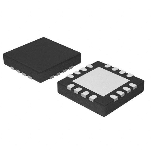
| 描述 | IC DETECTOR PHASE FREQ 24-QFN |
| 产品分类 | |
| 品牌 | Hittite Microwave Corporation |
| 数据手册 | |
| 产品图片 |
|
| 产品型号 | HMC984LP4E |
| RF类型 | 通用 |
| rohs | 无铅 / 符合限制有害物质指令(RoHS)规范要求 |
| 产品系列 | - |
| 其它名称 | 1127-1631 |
| 包装 | 剪带 |
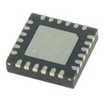
| 封装/外壳 | 24-VFQFN 裸露焊盘 |
| 标准包装 | 50 |
| 特色产品 | http://www.digikey.cn/product-highlights/zh/pll-chipset/52286 |
| 电压-电源 | 4.5 V ~ 5.5 V |
| 电流-电源 | 97mA |
| 精度 | - |
| 输入范围 | - |
| 频率 | 0Hz ~ 350MHz |


- 商务部:美国ITC正式对集成电路等产品启动337调查
- 曝三星4nm工艺存在良率问题 高通将骁龙8 Gen1或转产台积电
- 太阳诱电将投资9.5亿元在常州建新厂生产MLCC 预计2023年完工
- 英特尔发布欧洲新工厂建设计划 深化IDM 2.0 战略
- 台积电先进制程称霸业界 有大客户加持明年业绩稳了
- 达到5530亿美元!SIA预计今年全球半导体销售额将创下新高
- 英特尔拟将自动驾驶子公司Mobileye上市 估值或超500亿美元
- 三星加码芯片和SET,合并消费电子和移动部门,撤换高东真等 CEO
- 三星电子宣布重大人事变动 还合并消费电子和移动部门
- 海关总署:前11个月进口集成电路产品价值2.52万亿元 增长14.8%


PDF Datasheet 数据手册内容提取
HMC984LP4E v02.0112 DIGITAL PHASE-FREQUENCY DETECTOR Typical Applications Features The HMC984LP4E is suitable for: Ultra-Low Noise: • Test Equipment -231 dBc/Hz FOM Integer Mode T M • Portable Instruments -227 dBc/Hz FOM Fractional Mode S • High Performance Fractional-N Frequency Ultra Low Spurious Emissions: Synthesizers with Ultra Low Spurious Emissions - Less Than 60 dBc Fractional Spurious - S • Military Differential Phase Detector Input R 14-bit Reference Frequency Divider O Lock Indicator Output T Phase Measurement Capability C E GPIO (General Purpose Input/Output) Test Pin T Cycle Slip Prevention Support with HMC984LP4E E 24 pin, 4 x 4 mm, LP4E Package D & S R Functional Diagram General Description E D HMC984LP4E is a high-performance, ultra-low phase I noise, SiGe BiCMOS Phase-Frequency Detector V and Charge Pump targeted to be used together with I D the HMC983LP5E (Fractional Frequency Divider) to together form a high performance, low noise, ultra low Y spurious emission fractional-N frequency synthesizer. C N Although best performance and maximum features are achieved when used together with the HMC983LP5E, E the HMC984LP4E can also be used as a stand-alone, U low phase noise phase frequency detector. Q The HMC984LP4E can receive differential VCO input, E and a reference frequency as high as 150 MHz. It R features a 14-bit reference frequency R-Divider, and F automatic and/or configurable Lock Detect Indicator, as well as integrated CSP (Cycle Slip Prevention) capability, when used together with the HMC983LP5E, that significantly improves frequency lock time. Integrated Charge Pump phase swap option enables seamless interfaced to VCOs and active loop filters with inverted polarity. Additional features include adjustable Charge Pump gain and offset current that improve linearity and performance, and a Soft Reset feature that resets all register to default values without having to perform a power-cycle. The HMC984LP4E is housed in a compact 24 pin 4x4 mm LP4 package. Product covered by US and Foreign Patents including US Pat. No. 8,531,217. InfoFrmoarti opn rfuicrneish, edd eblyi vAenarlyog aDnevdic etso i sp blaelicevee do trod bee rasc:c uHraitet tiatned Mreliiacblreo. wHoawveveer ,C noo rpFoorra ptiroicne,, 2de Elivliezray,b aentdh tDo rpilvaece, Corhdeerlms: sAfnoarldog, MDeAv ic0e1s8, 2In4c., responsibility is assumed by Analog Devices for its use, nor for any infringements of patents or other One Technology Way, P.O. Box 9106, Norwood, MA 02062-9106 1 rliicgehntss eo fi sth girrda nptaerdti ebsy t himatp mlicaayt iorens 9uol7rt of8rtoh-me2r wit5sis 0ues -eu3.n dS3ep4re ca3infi yct aeptiaolt ne sn• ts ou rb9 jpe7act8te tno-t 2 crhi5gah0ntgs- e3o wf 3Ait7hnoa3ulot gfn aoDtixecve i .c •eNs o. OrPdheonr eO: 7n8-1l-in32e9 -a4t7 w00w (cid:127) wO.rhdeitrt iotnel.inceo amt www.analog.com Trademarks and registered trademarks are the property of their rAesppepcltiivce aowtinoerns. Support: appsA@pphliicttaittieon.c Soumpport: Phone: 1-800-ANALOG-D
HMC984LP4E v02.0112 DIGITAL PHASE-FREQUENCY DETECTOR Table 1. Electrical Specifications TA = +25 °C, AVDD, RVDD, VDDPD1, VDDPD2, DVDD = 3 V; VCCPD, VPPCP, VDDCP = 5 V; GND = 0 V T Parameter Conditions Min. Typ. Max. Units M Ref. Input Characteristics S Frequency Range DC 50 350 MHz - Ref. Input Power Range 50 Ω Source 6 12 dBm S Ref. Input Impedance 100||3 Ω||pF R Ref/-Divider Range (14-bit) 1 16383 O Phase Detector (PD) T C PD Input Internal Pull-Up Resistance VCOp, VCOn, Each Side 50 Ω E PD Input Current VCOp, VCOn, 2.5 mA Steps 12.5 15 17.5 mA T PD Input Voltage Swing Single-Ended Peak-to-Peak 625 750 875 mV E Fractional Mode D 12 dBm Sine-Wave Input, Mode A & B DC 50 125 MHz & Phase Detector Frequency 2 dBm Square-Wave Input, Mode A & B DC 50 90 MHz S Integer Mode R 12 dBm Sine-Wave Input DC 50 175 MHz E Phase Detector Frequency 2 dBm Square-Wave Input DC 50 150 MHz D Charge Pump (CP) I V 7-bit Programmable, 20 uA/Step, Charge CP Output Current 0.02 2.5 mA I Pump Gain = CP Current/2π Amps/rad D CP HiK See “Charge Pump High Gain (HiK) 3.5 6 mA Y Mode” section C Offset Current 7-bit Programmable,5 uA/Step 5 635 µA N Phase noise [1] E Integer Mode -230 dBc/Hz U Fractional Modes A & B -227 dBc/Hz Q Floor Figure of Merit (FOM) HiK Integer Mode -232 dBc/Hz E R HiK Fractional Mode A -230 dBc/Hz F HiK Fractional Mode B -229 dBc/Hz Integer Mode -269 dBc/Hz Fractional Modes A & B -267 dBc/Hz Flicker Figure of Merit (FOM) HiK Integer Mode -268 dBc/Hz HiK Fractional Mode A -266 dBc/Hz HiK Fractional Mode B -266 dBc/Hz Spurious [1] Frequency offsets less than loop band- Integer Boundary Spurs @ 2.1 GHz -60 -55 dBc width FPD=50 MHz, Mode A Frequency offsets less than loop band- Integer Boundary Spurs @ 2.1 GHz -70 -65 dBc width FPD=50 MHz, Mode B 1/2 Integer Boundary Spurs FPD=50 MHz -75 -70 dBc 1/3 Integer Boundary Spurs FPD=50 MHz -85 -80 dBc [1] Measured with HMC983LP5E/HMC984LP4E as fractional-N synthesizer chip set. InfoFrmoarti opn rfiucrneis,h edd eblyi vAenarlyog a Dnedvic etos isp blaelcievee do trod bee rasc:c uHraittet iatned Mreliiacbrleo. wHoawvevee r,C noo rpFoorra ptiroicne,, 2d eElivliezray,b aentdh tDo rpivlaec,e Corhdeelrms: sAfnoarldog, MDeAv ic0e1s8, 2In4c., responsibility is assumed by Analog Devices for its use, nor for any infringements of patents or other One Technology Way, P.O. Box 9106, Norwood, MA 02062-9106 2 rliicgehntss eo fi sth girrda nptaerdti ebsy t himatp mlicaayt iorens9 uo7lrt 8ofrtoh-me2r wi5tsis 0ues -eu3.n d3Sep4re c3ainf iyct aeptialo tne sn• ts ou 9rb jpe7ac8tte t-not2 cr5higah0ntgs- e3o wf3 Ait7hnoa3ulo t gfn aoDtxiecv ei .c •eN so . OrPdheorn eO: 7n8-1li-n32e9 a-4t7 w00w (cid:127)w O.rhdietrt iotenl.inceo amt www.analog.com Trademarks and registered trademarks are the property of their Arespppecltiivcea owtinoenrs. Support: appsA@pphliitctaittieo.nc Soumpport: Phone: 1-800-ANALOG-D
HMC984LP4E v02.0112 DIGITAL PHASE-FREQUENCY DETECTOR Table 1. Electrical Specifications Continued... TA = +25 °C, AVDD, RVDD, VDDPD1, VDDPD2, DVDD = 3 V; VCCPD, VPPCP, VDDCP = 5 V; GND = 0 V T Parameter Conditions Min. Typ. Max. Units M 1/5 Integer Boundary Spurs Fpd=50 MHz -85 dBc S Logic Inputs - VIH Input High Voltage DVDD - 0.4 V S VIL Input Low Voltage 0.4 V R Logic Outputs O VOH Output High Voltage DVDD- 0.4 V T VOL Output Low Voltage 0.4 V C DC Load 1.5 mA E T Serial Port E Serial Port Clock Frequency 30 MHz D Power Supplies & Analog Supplies, AVDD should equal AVDD, RVDD DVDD 2.8 3 3.3 V S VCCPD 5 V Analog Supply for PD 4.5 5 5.5 V R VPPCP CP Analog Supply 4.5 5 5.5 V E VDDCP CP Digital Supply 4.5 5 5.5 V D I DVDD, VDDPD1, VDDPD2 Digital Supplies 2.8 3 3.3 V V Current Consumption I D IDD- Total Current Consumption 123.6 mA Y I-AVDD (3 V) AVDD Current 4.8 mA C I-RVDD (3 V) Reference Path Current 22 mA N I-VCCPD (5 V) PD Current 83.5 mA E I-VDDPD1 (3 V) PD Digital Supply Current 2.7 mA U I-VDDPD2 (3 V) PD Digital Supply Current 2.7 mA Q I-VPPCP (5 V) CP Analog Supply Current 3 mA E R I-VDDCP (5 V) CP Digital Supply Current 2.9 mA F I-DVDD (3 V) Total DVDD Current 2 mA Bias Reference Voltage[2] Measured with 10 GΩ Volt Meter 1.58 1.72 1.86 V [2] Bias voltage cannot drive external load. It must be measured with a 10 GΩ voltmeter such as Agilent 34410A. A typical 10 MΩ Digital Volt Meter will read erroneously. InfoFrmoarti opn rfuicrneis,h edd eblyi vAenarlyog aDnevdic etso isp blaelicevee do trod bee rasc:c uHraitett iatned Mreliiacblreo. wHoawveveer ,C noo rpFoorra ptiroicne,, 2d eElivliezray,b aentdh tDo rpilvaec,e Corhdeerlms: sAfnoarldog, MDeAv ic0e1s8, 2In4c., responsibility is assumed by Analog Devices for its use, nor for any infringements of patents or other One Technology Way, P.O. Box 9106, Norwood, MA 02062-9106 rights of third parties that may res9ul7t f8ro-m2 i5ts 0us-e3. S3p4ec3if ictaetiol n s• s u b9je7c8t to- 2ch5a0ng-e3 w3it7ho3ut fnaotxice . •N o OrPdheonr eO: 7n8-1l-in32e9 a-4t7 w00w (cid:127) wO.rhdeitrt iotnel.inceo amt www.analog.com 6 - 3 license is granted by implication or otherwise under any patent or patent rights of Analog Devices. Trademarks and registered trademarks are the property of their Aresppepcltiivce aowtinoerns. Support: appsA@pphliicttaittieon.c Soumpport: Phone: 1-800-ANALOG-D
HMC984LP4E v02.0112 DIGITAL PHASE-FREQUENCY DETECTOR TYPICAL PERFORMANCE CHARACTERISTICS Figure 1. HMC984LP4E & HMC983LP5E Figure 2. HMC984LP4E & HMC983LP5E T PLL Flicker FOM vs Temperature [1] PLL Floor FOM vs Temperature [1] M S -266 -226 - -266.5 -227 Mode B Mode B S ECTOR FLICKER FOM (dBc/Hz)--22--66228766..5587 Hi K Mode B Hi K InInteteggeer rM Mooddee FLICKER FOM (dBc/Hz) ----222233221098 Hi K Mode B Integer ModeHi K Integer Mode T -269 -232 E -269.5 -233 D -50 -25 0 25 50 75 100 -50 -25 0 25 50 75 100 TEMPERATURE (C) TEMPERATURE (C) & Figure 3. HMC984LP4E & HMC983LP5E Figure 4. HMC984LP4E & HMC983LP5E S R PLL Flicker FOM vs Frequency [1] PLL Floor FOM vs Frequency [1] E -265.5 -226 D Hi K Mode B Hi K Mode A -266 -227 DIVI Bc/Hz)-2-6266.57 Mode A Bc/Hz) -228 Mode A HMi oKd Me oBde B Y FOM (d-267.5 Mode B FOM (d -229 Hi K Mode A R R -230 C CKE -268 Hi K Integer Mode CKE Integer Mode N FLI-268.5 FLI -231 Integer Mode E -269 -232 U Hi K Integer Mode -269.5 -233 Q 1 2 3 4 5 6 7 8 1 2 3 4 5 6 7 8 E FREQUENCY(GHz) FREQUENCY(GHz) R F Figure 5. HMC984LP4E & HMC983LP5E Figure 6. HMC984LP4E & HMC983LP5E PLL Flicker FOM vs Reference Power [1] PLL Floor FOM vs Reference Power [1] -264.5 -225 -265 -226 dBc/Hz)-2-6256.56 Mode B Bc/Hz) --222287 Mode B FOM (-266.5 Hi K Mode B OM (d -229 CKER -267 Hi K Integer Mode OOR F -230 Hi K Mode B FLI-267.5 FL -231 Integer Mode Integer Mode -268 -232 Hi K Integer Mode -268.5 -233 -15 -10 -5 0 5 10 15 -15 -10 -5 0 5 10 15 REFERENCE POWER (dBm) REFERENCE POWER (dBm) [1] Crystal frequency = 100 MHz, PFD frequency = 50 MHz, Active Loop Filter with 220 KHz Bandwidth. Measured at 4101 MHz in fractional mode and 4100 MHz in integer mode. InfoFrmoarti opn rfiucrneis,h edd eblyi vAenarlyog a Dnedvic etos isp blaelcievee do trod bee rasc:c uHraittet iatned Mreliiacbrleo. wHoawvevee r,C noo rpFoorra ptiroicne,, 2d eElivliezray,b aentdh tDo rpivlaec,e Corhdeelrms: sAfnoarldog, MDeAv ic0e1s8, 2In4c., responsibility is assumed by Analog Devices for its use, nor for any infringements of patents or other One Technology Way, P.O. Box 9106, Norwood, MA 02062-9106 4 rliicgehntss eo fi sth girrda nptaerdti ebsy t himatp mlicaayt iorens9 uo7lrt 8ofrtoh-me2r wi5tsis 0ues -eu3.n d3Sep4re c3ainf iyct aeptialo tne sn• ts ou 9rb jpe7ac8tte t-not2 cr5higah0ntgs- e3o wf3 Ait7hnoa3ulo t gfn aoDtxiecv ei .c •eN so . OrPdheorn eO: 7n8-1li-n32e9 a-4t7 w00w (cid:127)w O.rhdietrt iotenl.inceo amt www.analog.com Trademarks and registered trademarks are the property of their Arespppecltiivcea owtinoenrs. Support: appsA@pphliitctaittieo.nc Soumpport: Phone: 1-800-ANALOG-D
HMC984LP4E v02.0112 DIGITAL PHASE-FREQUENCY DETECTOR Figure 7. HMC984LP4E & HMC983LP5E Figure 8. HMC984LP4E & HMC983LP5E PLL Flicker FOM vs CP Current [2] PLL Floor FOM vs CP Current [2] -259 -218 -260 T -220 M OM (dBc/Hz)--226621 M (dBc/Hz)-222 - S ER F-263 R FO-224 S K O FLIC-264 FLO R -226 O -265 T -266 -228 C 0.5 0.75 1 1.25 1.5 1.75 2 2.25 2.5 0.5 0.75 1 1.25 1.5 1.75 2 2.25 2.5 E CHARGE PUMP CURRENT (mA) CHARGE PUMP CURRENT (mA) T E Figure 9. HMC984LP4E & HMC983LP5E Figure 10. HMC984LP4E & HMC983LP5E D PLL Flicker FOM vs CP Voltage [3] PLL Floor FOM vs CP Voltage [3] & -230 -195 -235 -200 S R -240 -205 CKER FOM (dBc/Hz) ---222554505 Hi K Mode B Hi K Integer MoMdeode B OOR FOM (dBc/Hz) ---222211050 IVIDE FLI -260 FL -225 Mode B Hi K Mode B D -265 -230 Y Integer Mode C -270 Integer Mode -235 Hi K Integer Mode 0 1 2 3 4 5 0 1 2 3 4 5 N CHARGE PUMP VOLTAGE (V) CHARGE PUMP VOLTAGE (V) E U Q Figure 11. HMC984LP4E & HMC983LP5E Figure 12. HMC984LP4E & HMC983LP5E E PLL Performance at 7000.01 MHz [4] PLL Performance at 4100.01 MHz [5] R -60 -60 F -80 -80 Bc/Hz)-100 Bc/Hz)-100 d d E ( E ( S-120 S-120 OI OI N N E E AS-140 AS-140 H H P P -160 -160 -180 -180 102 103 104 105 106 107 108 102 103 104 105 106 107 108 OFFSET FREQUENCY (Hz) OFFSET FREQUENCY (Hz) [2] PLL operated in Mode B, CP Votage = 2.5 V, Active Loop Filter with 220 kHz bandwidth used [3] Charge Pump Current = 2.5 mA [4] Crystal frequency=100MHz, PD frequency=50MHz, CP current=2.5mA, CP offset current=255 µA, Loop bandwidth = 87 kHz, PLL in Mode B. [5] Reference frequency=100 MHz, PD frequency=50 MHz, CP current=2.5 mA, CP offset current=280 µA, Loop bandwidth = 87 kHz, PLL in Mode B. InfoFrmoarti opn rfuicrneis,h edd eblyi vAenarlyog aDnevdic etso isp blaelicevee do trod bee rasc:c uHraitett iatned Mreliiacblreo. wHoawveveer ,C noo rpFoorra ptiroicne,, 2d eElivliezray,b aentdh tDo rpilvaec,e Corhdeerlms: sAfnoarldog, MDeAv ic0e1s8, 2In4c., responsibility is assumed by Analog Devices for its use, nor for any infringements of patents or other One Technology Way, P.O. Box 9106, Norwood, MA 02062-9106 rights of third parties that may res9ul7t f8ro-m2 i5ts 0us-e3. S3p4ec3if ictaetiol n s• s u b9je7c8t to- 2ch5a0ng-e3 w3it7ho3ut fnaotxice . •N o OrPdheonr eO: 7n8-1l-in32e9 a-4t7 w00w (cid:127) wO.rhdeitrt iotnel.inceo amt www.analog.com 6 - 5 license is granted by implication or otherwise under any patent or patent rights of Analog Devices. Trademarks and registered trademarks are the property of their Aresppepcltiivce aowtinoerns. Support: appsA@pphliicttaittieon.c Soumpport: Phone: 1-800-ANALOG-D
HMC984LP4E v02.0112 DIGITAL PHASE-FREQUENCY DETECTOR Figure 13. HMC984LP4E & HMC983LP5E Figure 14. HMC984LP4E & HMC983LP5E [6] PLL Performance at 2100.01 MHz [6] -60 -80 T -80 -100 M Calculated PLL Mode B RS - S HASE NOISE (dBc/Hz)---111420000 HASE NOISE (dBc/Hz)--114200 Simulated Mode B CalculateMd ePaLsLu rInetde g Mero dMeo Bde P P O -160 -160 Simulated Integer Mode T Measured Integer Mode C -180 -180 102 103 104 105 106 107 108 102 103 104 105 106 107 108 E OFFSET FREQUENCY (Hz) OFFSET FREQUENCY (Hz) T E Figure 15. HMC984LP4E & HMC983LP5E PLL Figure 16. HMC984LP4E & HMC983LP5E D In Band Fractional Spurs vs. Offset Current [8] PLL Floor FOM vs. RF Input Power & -20 -20 -226 Y DIVIDERS D SPUR AT 15 kHz OFFSET (dBc/Hz)-1---08640000 445470000000 MMMHHHzzz ----186400000PHASE NOISE (dBc/Hz) FLOOR FOM (dBc/Hz)-----222223322210987 HHii M KKoM MMdoeood ddBeee A AB C BAN -232 Integer Mode Hi K Integer Mode N I -120 -120 -233 N -800 -600 -400 -200 0 200 400 600 800 -30 -25 -20 -15 -10 -5 0 5 10 E OFFSET CURRENT (mA) RF INPUT POWER (dBm) U Q Figure 17. HMC984LP4E & HMC983LP5E Figure 18. HMC984LP4E & HMC983LP5E E PLL Flicker FOM vs. RF Input Power PLL Two-Way Auto Frequency Sweep [9] R -264.5 7000 F -265 Mode B 6900 -265.5 Bc/Hz) -266 Mode A MHz) 6800 OM (d-266.5 Hi K Mode B Hi K Mode A NCY ( 6700 F E KER -267 EQU 6600 C Hi K Integer Mode R LI F F-267.5 6500 -268 Integer Mode -268.5 6400 -30 -25 -20 -15 -10 -5 0 5 10 0 5 10 15 20 TIME (ms) RF INPUT POWER (dBm) [6] Crystal frequency=100 MHz, PFD frequency=50 MHz, CP current=2.5 mA, CP offset current=280 µA, Loop bandwidth = 87 kHz, PLL Mode [7] Measured at 7 GHz in Integer Mode and 7.001 GHz in Fractional mode B. PD Frequency = 50 MHz, and loop filter BW = 87 kHz. Simulated results were obtained using Hittite PLL Design software. [8] Active Loop filter bandwidth 150 kHz, measured at 10 kHz offset, PFD Frequency=50 MHz. Offset polarity should be positive for inverting configurations and negative otherwise. [9] 50 MHz PFD InfoFrmoarti opn rfiucrneis,h edd eblyi vAenarlyog a Dnedvic etos isp blaelcievee do trod bee rasc:c uHraittet iatned Mreliiacbrleo. wHoawvevee r,C noo rpFoorra ptiroicne,, 2d eElivliezray,b aentdh tDo rpivlaec,e Corhdeelrms: sAfnoarldog, MDeAv ic0e1s8, 2In4c., responsibility is assumed by Analog Devices for its use, nor for any infringements of patents or other One Technology Way, P.O. Box 9106, Norwood, MA 02062-9106 6 rliicgehntss eo fi sth girrda nptaerdti ebsy t himatp mlicaayt iorens9 uo7lrt 8ofrtoh-me2r wi5tsis 0ues -eu3.n d3Sep4re c3ainf iyct aeptialo tne sn• ts ou 9rb jpe7ac8tte t-not2 cr5higah0ntgs- e3o wf3 Ait7hnoa3ulo t gfn aoDtxiecv ei .c •eN so . OrPdheorn eO: 7n8-1li-n32e9 a-4t7 w00w (cid:127)w O.rhdietrt iotenl.inceo amt www.analog.com Trademarks and registered trademarks are the property of their Arespppecltiivcea owtinoenrs. Support: appsA@pphliitctaittieo.nc Soumpport: Phone: 1-800-ANALOG-D
HMC984LP4E v02.0112 DIGITAL PHASE-FREQUENCY DETECTOR Figure 19. HMC984LP4E & HMC983LP5E PLL Figure 20. HMC984LP4E & HMC983LP5E PLL One-Way Triggered Frequency Sweep [10] Floor FOM Vs. Sine-Wave Ref Input Level [11] 7000 -210 6900 T M -215 FREQUENCY (MHz) 666678000000 FLOOR FOM (dBc/Hz) --222250 50 MHz 25 MHz 12.5 MHz RS - S 6500 O 100 MHz T 6400 -230 C 0 200 400 600 800 1000 -15 -10 -5 0 5 TIME (ms) REFERENCE POWER (dBm) E T E Figure 21. HMC984LP4E & HMC983LP5E PLL Figure 22. HMC984LP4E & HMC983LP5E D Floor FOM Vs Square-Wave Ref Input Level [11] PLL Reference Input Return Loss [12] & -216 -6 S -218 100 MHz -8 R Hz) -220 B) E FLOOR FOM (dBc/ --222242 50 MHz RETURN LOSS (d--1120 DIVID -226 12.5 MHz -14 Y 25 MHz C -228 -16 -15 -10 -5 0 5 0 100 200 300 400 500 600 N REFERENCE POWER (dBm) FREQUENCY (MHz) E U Figure 23. HMC984LP4E & HMC983LP5E Figure 24. HMC984LP4E & HMC983LP5E Q PLL Cycle Slip Prevention at 100 MHz PD [13] PLL Cycle Slip Prevention at 50 MHz PD [13] E 7050 7050 R PLL OUTPUT FREQUENCY (MHz)666667788990505050000000 CRSegP0 EEnha[1b8le:1d5 ] =CR 8SehgP0 EEnha[1b8le:1d5 ] = 1Chycle Slip Disabled PLL OUTPUT FREQUENCY (GHz) 666667788990505050000000 CRSegP0 EEnha[1b8le:1d5 ] = 8h Cycle Slip Disabled CRSegP0 EEnha[1b8le:1d5 ] = 1h F 6700 6700 0 50 100 150 200 250 300 0 50 100 150 200 250 300 TIME (us) TIME (us) [10] Using 10 Hz external trigger. PFD frequency = 10 MHz. Measured with HMC983LP5E/HMC984LP4E fractional-N synthesizer chip set. [11] Measured with a 100 Ω external resistor termination, resulting in 50 Ω effective input impedance of Reference. Full FOM performance up to maximum 3.3 Vpp input voltage. [12] Measured with 100 Ω external termination AC coupled on HMC984LP4E & HMC983LP5E evaluation board. [13]Measured with HMC983LP5E/HMC984LP4E chip set as fractional-N synthesizer. Crystal input frequency = 100 MHz, CP current = 2.5 mA, CP offset current = 245 uA, Loop filter bandwidth = 87 KHz, DSM Mode B selected. Cycle Slip Prevention (CSP) is disabled in HMC984LP4E by setting Reg 01h [4] = 0. Setting Reg 01h [4] = 1 enables CSP in the two chip PLL. InfoFrmoarti opn rfuicrneis,h edd eblyi vAenarlyog aDnevdic etso isp blaelicevee do trod bee rasc:c uHraitett iatned Mreliiacblreo. wHoawveveer ,C noo rpFoorra ptiroicne,, 2d eElivliezray,b aentdh tDo rpilvaec,e Corhdeerlms: sAfnoarldog, MDeAv ic0e1s8, 2In4c., responsibility is assumed by Analog Devices for its use, nor for any infringements of patents or other One Technology Way, P.O. Box 9106, Norwood, MA 02062-9106 rights of third parties that may res9ul7t f8ro-m2 i5ts 0us-e3. S3p4ec3if ictaetiol n s• s u b9je7c8t to- 2ch5a0ng-e3 w3it7ho3ut fnaotxice . •N o OrPdheonr eO: 7n8-1l-in32e9 a-4t7 w00w (cid:127) wO.rhdeitrt iotnel.inceo amt www.analog.com 6 - 7 license is granted by implication or otherwise under any patent or patent rights of Analog Devices. Trademarks and registered trademarks are the property of their Aresppepcltiivce aowtinoerns. Support: appsA@pphliicttaittieon.c Soumpport: Phone: 1-800-ANALOG-D
HMC984LP4E v02.0112 DIGITAL PHASE-FREQUENCY DETECTOR Table 2. Pin Descriptions Pin Number Function Description Interface Schematic T M S 1 REF_EN Gate control output for TCXO clock export - S R O T C E T E 2 DTSTO Lock Detect/GPIO bit 0 D & S R E D I V 3 VCOp Positive Input Pin for PFD I D Y C N E U Q E R 4 VCOn Negative Input Pin for PFD F 5 VCCPD 5 V Analog Supply for Differential PFD 6,7 VDDPD1, VDDPD2 3 V Phase Detector Supply 1, 3 V Phase Detector Supply 2 8 VDDCP 5 V Charge Pump Supply InfoFrmoarti opn rfiucrneis,h edd eblyi vAenarlyog a Dnedvic etos isp blaelcievee do trod bee rasc:c uHraittet iatned Mreliiacbrleo. wHoawvevee r,C noo rpFoorra ptiroicne,, 2d eElivliezray,b aentdh tDo rpivlaec,e Corhdeelrms: sAfnoarldog, MDeAv ic0e1s8, 2In4c., responsibility is assumed by Analog Devices for its use, nor for any infringements of patents or other One Technology Way, P.O. Box 9106, Norwood, MA 02062-9106 8 rliicgehntss eo fi sth girrda nptaerdti ebsy t himatp mlicaayt iorens9 uo7lrt 8ofrtoh-me2r wi5tsis 0ues -eu3.n d3Sep4re c3ainf iyct aeptialo tne sn• ts ou 9rb jpe7ac8tte t-not2 cr5higah0ntgs- e3o wf3 Ait7hnoa3ulo t gfn aoDtxiecv ei .c •eN so . OrPdheorn eO: 7n8-1li-n32e9 a-4t7 w00w (cid:127)w O.rhdietrt iotenl.inceo amt www.analog.com Trademarks and registered trademarks are the property of their Arespppecltiivcea owtinoenrs. Support: appsA@pphliitctaittieo.nc Soumpport: Phone: 1-800-ANALOG-D
HMC984LP4E v02.0112 DIGITAL PHASE-FREQUENCY DETECTOR Table 2. Pin Descriptions Continued... Pin Number Function Description Interface Schematic T M S - 9 CP Charge Pump Output Pin S R O T C E 10 VPPCP 5 V Analog Power Supply Pin Charge Pump T 11 AVDD 3 V Analog Supply E 12 BIAS External Decoupling for Analog Bias Circuits D 13 RVDD 3 V Supply Pin for Reference Circuits & S R E D 14 XREFP Reference/TCXO Input Pin I V I D Y C N 15 NC No Connect Pin E 16 DVDD 3 V Digital Supply Pin U Q E R 17 CEN Chip Enable Pin F 18 SDO Serial Data Output Pin InfoFrmoarti opn rfuicrneis,h edd eblyi vAenarlyog aDnevdic etso isp blaelicevee do trod bee rasc:c uHraitett iatned Mreliiacblreo. wHoawveveer ,C noo rpFoorra ptiroicne,, 2d eElivliezray,b aentdh tDo rpilvaec,e Corhdeerlms: sAfnoarldog, MDeAv ic0e1s8, 2In4c., responsibility is assumed by Analog Devices for its use, nor for any infringements of patents or other One Technology Way, P.O. Box 9106, Norwood, MA 02062-9106 rights of third parties that may res9ul7t f8ro-m2 i5ts 0us-e3. S3p4ec3if ictaetiol n s• s u b9je7c8t to- 2ch5a0ng-e3 w3it7ho3ut fnaotxice . •N o OrPdheonr eO: 7n8-1l-in32e9 a-4t7 w00w (cid:127) wO.rhdeitrt iotnel.inceo amt www.analog.com 6 - 9 license is granted by implication or otherwise under any patent or patent rights of Analog Devices. Trademarks and registered trademarks are the property of their Aresppepcltiivce aowtinoerns. Support: appsA@pphliicttaittieon.c Soumpport: Phone: 1-800-ANALOG-D
HMC984LP4E v02.0112 DIGITAL PHASE-FREQUENCY DETECTOR Table 2. Pin Descriptions Continued... Pin Number Function Description Interface Schematic T M S 19, SENb, Serial Port Enable Input Pin, Active Low, - 20, SDI, Serial Port Data Input Pin, S R 21 SCLK Serial Data Clock Input Pin O T C E T E D & 22 CHIP3 Chip Address Bit 3 S R E D I V I D Y 23 UPSAT Reference Saturation Output C N E U Q E R F VCO Saturation Output Flag 24 DNSAT Also Multiplexed with Crystal Oscillator Clock InfoFrmoarti opn rfiucrneis,h edd eblyi vAenarlyog a Dnedvic etos isp blaelcievee do trod bee rasc:c uHraittet iatned Mreliiacbrleo. wHoawvevee r,C noo rpFoorra ptiroicne,, 2d eElivliezray,b aentdh tDo rpivlaec,e Corhdeelrms: sAfnoarldog, MDeAv ic0e1s8, 2In4c., responsibility is assumed by Analog Devices for its use, nor for any infringements of patents or other One Technology Way, P.O. Box 9106, Norwood, MA 02062-9106 10 rliicgehntss eo fi sth girrda nptaerdti ebsy t himatp mlicaayt iorens9 uo7lrt 8ofrtoh-me2r wi5tsis 0ues -eu3.n d3Sep4re c3ainf iyct aeptialo tne sn• ts ou 9rb jpe7ac8tte t-not2 cr5higah0ntgs- e3o wf3 Ait7hnoa3ulo t gfn aoDtxiecv ei .c •eN so . OrPdheorn eO: 7n8-1li-n32e9 a-4t7 w00w (cid:127)w O.rhdietrt iotenl.inceo amt www.analog.com Trademarks and registered trademarks are the property of their Arespppecltiivcea owtinoenrs. Support: appsA@pphliitctaittieo.nc Soumpport: Phone: 1-800-ANALOG-D
HMC984LP4E v02.0112 DIGITAL PHASE-FREQUENCY DETECTOR Table 19. Absolute Maximum Ratings Max VDC to Paddle on Supply Pins 6, Reflow Soldering -0.3 to 3.6 V 7, 11, 13, 16 Peak Temperature 260 °C Time at Peak Temperature 40 s T VCCPD, VPPCP, VDDCP -0.3 to +5.5 V M ESD Sensitivity (HBM) Class 1 B VCOp, VCOn Common Mode Voltage VCCPD - 1.4 V S XREFP 50 Ω Source + 12 dBm - Digital Input Voltage Range 0.25 to DVDD + 0.5 V Stresses above those listed under Absolute Maximum Ratings may S Digital Load 1 kΩ Minimum cause permanent damage to the device. This is a stress rating only; R functional operation of the device at these or any other conditions Operating Temperature Range -40 to +85 °C above those indicated in the operational section of this specification O Operating Temperature Range -65 to +125 °C is not implied. Exposure to absolute maximum rating conditions for T Maximum Junction Temperature 125 °C extended periods may affect device reliability. C Storage Temperature -65 to +125 °C E Thermal Resistance (Rth) ELECTROSTATIC SENSITIVE DEVICE (junction to ground paddle) 12 °C/W OBSERVE HANDLING PRECAUTIONS T E D Outline Drawing & S R E D I V I D Y C N E U Q E R NOTES: F [1] PACKAGE BODY MATERIAL: LOW STRESS INJECTION MOLDED PLASTIC SILICA AND SILICON IMPREGNATED. [2] LEAD AND GROUND PADDLE MATERIAL: COPPER ALLOY. [3] LEAD AND GROUND PADDLE PLATING: 100% MATTE TIN. [4] DIMENSIONS ARE IN INCHES [MILLIMETERS]. [5] LEAD SPACING TOLERANCE IS NON-CUMULATIVE. [6] PAD BURR LENGTH SHALL BE 0.15mm MAX. PAD BURR HEIGHT SHALL BE 0.25m MAX. [7] PACKAGE WARP SHALL NOT EXCEED 0.05mm [8] ALL GROUND LEADS AND GROUND PADDLE MUST BE SOLDERED TO PCB RF GROUND. [9] REFER TO HITTITE APPLICATION NOTE FOR SUGGESTED PCB LAND PATTERN. Package Information Part Number Package Body Material Lead Finish MSL Rating [2] Package Marking [1] H984 HMC984LP4E RoHS-compliant Low Stress Injection Molded Plastic 100% matte Sn MSL1 XXXX [1] 4-Digit lot number XXXX [2] Max peak reflow temperature of 260 °C InfoFrmoarti opn rfuicrneis,h edd eblyi vAenarlyog aDnevdic etso isp blaelicevee do trod bee rasc:c uHraitett iatned Mreliiacblreo. wHoawveveer ,C noo rpFoorra ptiroicne,, 2d eElivliezray,b aentdh tDo rpilvaec,e Corhdeerlms: sAfnoarldog, MDeAv ic0e1s8, 2In4c., responsibility is assumed by Analog Devices for its use, nor for any infringements of patents or other One Technology Way, P.O. Box 9106, Norwood, MA 02062-9106 rights of third parties that may res9ul7t f8ro-m2 i5ts 0us-e3. S3p4ec3if ictaetiol n s• s u b9je7c8t to- 2ch5a0ng-e3 w3it7ho3ut fnaotxice . •N o OrPdheonr eO: 7n8-1l-in32e9 a-4t7 w00w (cid:127) wO.rhdeitrt iotnel.inceo amt www.analog.com 6 - 11 license is granted by implication or otherwise under any patent or patent rights of Analog Devices. Trademarks and registered trademarks are the property of their Aresppepcltiivce aowtinoerns. Support: appsA@pphliicttaittieon.c Soumpport: Phone: 1-800-ANALOG-D
HMC984LP4E v02.0112 DIGITAL PHASE-FREQUENCY DETECTOR Evaluation PCB T M S - S R O T C E T E D & S R E D I V I D Y C N E U Q E R F The circuit board used in the application should use RF circuit design techniques. Signal lines should have 50 Ohms impedance while the package ground leads and exposed paddle should be connected directly to the ground plane similar to that shown unless mentioned otherwise. A sufficient number of via holes should be used to connect the top and bottom ground planes. The evaluation circuit board shown is available from Hittite upon request. Table 20. Evaluation Order Information Item Contents Part Number HMC984LP4E and HMC983LP5E PLL Chipset Evaluation PCB USB Interface Board Evaluation Kit EKIT01-HMC983LP5E 6’ USB A Male to USB B Female Cable CD ROM (Contains User Manual, Evaluation PCB Schematic, Evaluation Software) InfoFrmoarti opn rfiucrneis,h edd eblyi vAenarlyog a Dnedvic etos isp blaelcievee do trod bee rasc:c uHraittet iatned Mreliiacbrleo. wHoawvevee r,C noo rpFoorra ptiroicne,, 2d eElivliezray,b aentdh tDo rpivlaec,e Corhdeelrms: sAfnoarldog, MDeAv ic0e1s8, 2In4c., responsibility is assumed by Analog Devices for its use, nor for any infringements of patents or other One Technology Way, P.O. Box 9106, Norwood, MA 02062-9106 12 rliicgehntss eo fi sth girrda nptaerdti ebsy t himatp mlicaayt iorens9 uo7lrt 8ofrtoh-me2r wi5tsis 0ues -eu3.n d3Sep4re c3ainf iyct aeptialo tne sn• ts ou 9rb jpe7ac8tte t-not2 cr5higah0ntgs- e3o wf3 Ait7hnoa3ulo t gfn aoDtxiecv ei .c •eN so . OrPdheorn eO: 7n8-1li-n32e9 a-4t7 w00w (cid:127)w O.rhdietrt iotenl.inceo amt www.analog.com Trademarks and registered trademarks are the property of their Arespppecltiivcea owtinoenrs. Support: appsA@pphliitctaittieo.nc Soumpport: Phone: 1-800-ANALOG-D
HMC984LP4E v02.0112 DIGITAL PHASE-FREQUENCY DETECTOR Evaluation PCB Block Diagram T M S - S R O T C E T E D & S R E D I V I D Y C N E U Q E R F InfoFrmoarti opn rfuicrneis,h edd eblyi vAenarlyog aDnevdic etso isp blaelicevee do trod bee rasc:c uHraitett iatned Mreliiacblreo. wHoawveveer ,C noo rpFoorra ptiroicne,, 2d eElivliezray,b aentdh tDo rpilvaec,e Corhdeerlms: sAfnoarldog, MDeAv ic0e1s8, 2In4c., responsibility is assumed by Analog Devices for its use, nor for any infringements of patents or other One Technology Way, P.O. Box 9106, Norwood, MA 02062-9106 rights of third parties that may res9ul7t f8ro-m2 i5ts 0us-e3. S3p4ec3if ictaetiol n s• s u b9je7c8t to- 2ch5a0ng-e3 w3it7ho3ut fnaotxice . •N o OrPdheonr eO: 7n8-1l-in32e9 a-4t7 w00w (cid:127) wO.rhdeitrt iotnel.inceo amt www.analog.com 6 - 13 license is granted by implication or otherwise under any patent or patent rights of Analog Devices. Trademarks and registered trademarks are the property of their Aresppepcltiivce aowtinoerns. Support: appsA@pphliicttaittieon.c Soumpport: Phone: 1-800-ANALOG-D
HMC984LP4E v02.0112 DIGITAL PHASE-FREQUENCY DETECTOR Typical Performance Characteristics Theory of Operation T M Primary target application of the HMC984LP4E is to be used with the HMC983LP5E as shown in Figure 25. Together S these two components form a high performance, low noise, ultra low spurious emissions fractional-N frequency synthesizer. The two components are separated in order to maximize isolation between them, and minimize common - distortion and modulation by-products that exist in all PLLs. Careful IC design and increased isolation between the S two components result in high performance , high spectral efficiency PLL, with extremely low spurious emissions. R O T C E T E D & S R E D Figure 25. Typical Application of HMC984LP4E with HMC983LP5E to Form a Frequency Synthesizer I HMC984LP4E is a high performance low noise phase detector and charge pump. It consists of the following main V functional blocks; I D 1. Reference/Crystal Buffer Y 2. Reference Path ’R’ Divider C 3. Differential Phase/Frequency Detector N E 4. 5 V Charge Pump U 5. Two Lock Detect Circuits Q 6. Serial Port Interface E R PLL Performance Metrics (Figure of Merit, Noise Floor, and Flicker Noise Models) F The phase noise of an ideal phase locked oscillator is dependent upon a number of factors: a. Frequency of the VCO, and the Phase detector b. VCO Sensitivity, kvco, and VCO and Reference Oscillator phase noise profiles c. Charge Pump current, Loop Filter and Loop Bandwidth d. Mode of Operation: Integer, Fractional modulator style The contributions of the PLL to the output phase noise can be characterized in terms of a Figure of Merit (FOM) for both the PLL noise floor and the PLL flicker (1/f) noise regions, as follows: PLL PHASE F f2 F f2 NOISE Φ2p(f0,fm,fpd)= pf10 + pf00 (Eq 1) m pd InfoFrmoarti opn rfiucrneis,h edd eblyi vAenarlyog a Dnedvic etos isp blaelcievee do trod bee rasc:c uHraittet iatned Mreliiacbrleo. wHoawvevee r,C noo rpFoorra ptiroicne,, 2d eElivliezray,b aentdh tDo rpivlaec,e Corhdeelrms: sAfnoarldog, MDeAv ic0e1s8, 2In4c., responsibility is assumed by Analog Devices for its use, nor for any infringements of patents or other One Technology Way, P.O. Box 9106, Norwood, MA 02062-9106 14 rliicgehntss eo fi sth girrda nptaerdti ebsy t himatp mlicaayt iorens9 uo7lrt 8ofrtoh-me2r wi5tsis 0ues -eu3.n d3Sep4re c3ainf iyct aeptialo tne sn• ts ou 9rb jpe7ac8tte t-not2 cr5higah0ntgs- e3o wf3 Ait7hnoa3ulo t gfn aoDtxiecv ei .c •eN so . OrPdheorn eO: 7n8-1li-n32e9 a-4t7 w00w (cid:127)w O.rhdietrt iotenl.inceo amt www.analog.com Trademarks and registered trademarks are the property of their Arespppecltiivcea owtinoenrs. Support: appsA@pphliitctaittieo.nc Soumpport: Phone: 1-800-ANALOG-D
HMC984LP4E v02.0112 DIGITAL PHASE-FREQUENCY DETECTOR where: Ф 2 Phase Noise Contribution of the PLL (rads2/Hz) p f Frequency of the VCO (Hz) o f Frequency of the Phase Detector (Hz) T pd f Frequency offset from the carrier (Hz) M m Fpo Figure of Merit (FOM) for the phase noise floor S Fp1 Figure of Merit (FOM) for the flicker noise region - S R O T C E T E D & S R E D Figure 26. Figure of Merit Noise Models for the PLL I V If the free running phase noise of the VCO is known, it may also be represented by a figure of merit for both 1/f2 , F , I v2 D and the 1/f3, F , regions. v3 Y C VCO PHASE Φ2(f ,f )= Fν2f02 +Fν3f02 (Eq 2) N NOISE ν 0 m fm2 fm3 E U The Figures of Merit are essentially normalized noise parameters for both the PLL and VCO that can allow quick Q estimates of the performance levels of the PLL at the required VCO, offset and phase detector fre quency. Normally, E the PLL IC noise dominates inside the closed loop bandwidth of the synthesizer, and the VCO dominates outside the R loop bandwidth at offsets far from the carrier. Hence a quick estimate of the closed loop performance of the PLL can F be made by setting the loop bandwidth equal to the frequency where the PLL and free running phase noise are equal. The Figure of Merit is also useful in estimating the noise parameters to be entered into a closed loop design tool such as Hittite PLL Design, which can give a more accurate estimate of the closed loop phase noise and PLL loop filter component values. Given an optimum loop design, the approximate closed loop performance is simply given by the minimum of the PLL and VCO noise contributions. Φ2 =min(Φ2,Φ2) (Eq 3) p ν InfoFrmoarti opn rfuicrneis,h edd eblyi vAenarlyog aDnevdic etso isp blaelicevee do trod bee rasc:c uHraitett iatned Mreliiacblreo. wHoawveveer ,C noo rpFoorra ptiroicne,, 2d eElivliezray,b aentdh tDo rpilvaec,e Corhdeerlms: sAfnoarldog, MDeAv ic0e1s8, 2In4c., responsibility is assumed by Analog Devices for its use, nor for any infringements of patents or other One Technology Way, P.O. Box 9106, Norwood, MA 02062-9106 rights of third parties that may res9ul7t f8ro-m2 i5ts 0us-e3. S3p4ec3if ictaetiol n s• s u b9je7c8t to- 2ch5a0ng-e3 w3it7ho3ut fnaotxice . •N o OrPdheonr eO: 7n8-1l-in32e9 a-4t7 w00w (cid:127) wO.rhdeitrt iotnel.inceo amt www.analog.com 6 - 15 license is granted by implication or otherwise under any patent or patent rights of Analog Devices. Trademarks and registered trademarks are the property of their Aresppepcltiivce aowtinoerns. Support: appsA@pphliicttaittieon.c Soumpport: Phone: 1-800-ANALOG-D
HMC984LP4E v02.0112 DIGITAL PHASE-FREQUENCY DETECTOR An example of the use of the FOM values to make a quick estimate of PLL performance: Estimate the phase noise of an 7 GHz closed loop PLL with a 100 MHz reference operating in Fractional Mode B with the VCO operating at 7 GHz. Assume an HMC505LP4E VCO has free running phase noise in the 1/f2 region at 1 MHz offset of -130 dBc/Hz and T phase noise in the 1/f3 region at 1 kHz offset of -48 dBc/Hz. M F = -130 Free Running VCO PN at 1 MHz offset v1_dB S +20*log10(1e6) PNoise normalized to 1 Hz offset -20*log10(7e9) PNoise normalized to 1 Hz carrier - = -206.9 dBc/Hz at 1 Hz VCO FOM S R F = -48 Free Running VCO PN at 1 kHz offset v3_dB O +30*log10(1e3) PNoise normalized to 1 Hz offset T -20*log10(7e9) Pnoise normalized to 1 Hz carrier C = -154.9 dBc/Hz at 1 Hz VCO Flicker FOM We can see from Figure 3 and Figure 4 respectively that the PLL FOM floor and FOM flicker parameters in fractional E Mode A are approximately: T E Fpo_dB = -227 dBc/Hz at 1 Hz D Fp1_dB = -267 dBc/Hz at 1 Hz & Each of the Figure of Merit equations result in straight lines on a log-frequency plot. We can see in the example below S the resulting R PLL floor at 7 GHz = F + 20log10(fvco) - 10log10(fpd) = -227+ 196.9 -80 = -110.1 dBc/Hz po_dB E PLL Flicker at 1 kHz = F + 20log10(fvco) - 10log10(fm) = -267 + 196.9-30 = -100.1 dBc/Hz p1_dB D I VCO at 1 MHz = Fv1_dB + 20log10(fvco) - 20log10(fm) = -206.9 +196.9-120 = -130 dBc/Hz V VCO flicker at 1 kHz = F +20log10(fvco)-30log10(fm)= -154.9 +196.9-90 = -48 dBc/Hz v3_dB I D These four values help to visualize the main contributors to phase noise in the closed loop PLL. Each falls on a linear Y line on the log-frequency phase noise plot shown in Figure 25. C N Spurious Performance E U Q Integer Operation E The VCO always operates at an integer multiple of the PD frequency in an integer PLL. In general, spurious signals R originating from an integer PLL can only occur at multiples of the PD frequency. These unwanted outputs are often F simply referred to as reference sidebands. Spurs unrelated to the reference frequency must originate from outside sources. External spurious sources can modulate the VCO indirectly through power supplies, ground, or output ports, or bypass the loop filter due to poor isolation of the filter. It can also simply add to the output of the PLL. The HMC984LP4E together with the HMC983LP5E have been designed and tested for ultra-low spurious performance. Reference spuri ous levels can be typically below -100 dBc with a well designed board layout. A regulator with low noise and high power supply rejection, such as the HMC860LP3E, is recommended to minimize external spurious sources. Reference spurious levels of below -100 dBc require superb board isolation of power supplies, isolation of the VCO from the digital switching of the synthesizer and isolation of the VCO load from the PLL. Typical board layout, regulator design, demo boards and application information are available for very low spurious operation. Operation with lower levels of isolation in the application circuit board, from those rec ommended by Hittite, can result in higher spurious levels. InfoFrmoarti opn rfiucrneis,h edd eblyi vAenarlyog a Dnedvic etos isp blaelcievee do trod bee rasc:c uHraittet iatned Mreliiacbrleo. wHoawvevee r,C noo rpFoorra ptiroicne,, 2d eElivliezray,b aentdh tDo rpivlaec,e Corhdeelrms: sAfnoarldog, MDeAv ic0e1s8, 2In4c., responsibility is assumed by Analog Devices for its use, nor for any infringements of patents or other One Technology Way, P.O. Box 9106, Norwood, MA 02062-9106 16 rliicgehntss eo fi sth girrda nptaerdti ebsy t himatp mlicaayt iorens9 uo7lrt 8ofrtoh-me2r wi5tsis 0ues -eu3.n d3Sep4re c3ainf iyct aeptialo tne sn• ts ou 9rb jpe7ac8tte t-not2 cr5higah0ntgs- e3o wf3 Ait7hnoa3ulo t gfn aoDtxiecv ei .c •eN so . OrPdheorn eO: 7n8-1li-n32e9 a-4t7 w00w (cid:127)w O.rhdietrt iotenl.inceo amt www.analog.com Trademarks and registered trademarks are the property of their Arespppecltiivcea owtinoenrs. Support: appsA@pphliitctaittieo.nc Soumpport: Phone: 1-800-ANALOG-D
HMC984LP4E v02.0112 DIGITAL PHASE-FREQUENCY DETECTOR Of course, if the application environment contains other interfering frequencies unrelated to the PD fre quency, and if the application isolation from the board layout and regulation are insufficient, then the unwanted interfering frequencies will mix with the desired PLL output and cause additional spurs. The level of these spurs is dependant upon isolation and supply regulation or rejection (PSRR). T M Fractional Operation S - Unlike an integer PLL, spurious signals in a fractional PLL can occur due to the fact that the VCO operates at S frequencies unrelated to the PD frequency. Hence intermodulation of the VCO and the PD harmonics can cause spurious sidebands. Spurious emissions are largest when the VCO operates very close to an integer multiple of the R PD. When the VCO operates exactly at a harmonic of the PD then, no in-close mixing products are present. O T Interference is always present at multiples of the PD frequency, fpd, and the VCO frequency, fvco. If the fractional mode C of operation is used, the difference, Δ, between the VCO frequency and the nearest har monic of the reference, will E create what are referred to as integer boundary spurs. Depending upon the mode of operation of the PLL, higher T order, lower power spurs may also occur at multiples of integer fractions (sub-harmonics) of the PD frequency. That is, E fractional VCO frequencies which are near n·f + f ·d/m, where n, d and m are all integers and d≤m (mathematicians pd pd D refer to d/m as a rational num ber). We will refer to f d/m as an integer fraction. The denominator, m, is the order of pd the spurious product. Higher values of m produce smaller amplitude spurious at offsets of mΔ and usually when m>4 & spurs are small or unmeasurable. S The worst case, in fractional mode, is when d=1, and the VCO frequency is offset from n·f by less than the loop R pd bandwidth. This is the “in-band fractional boundary” case. E D I V I D Y C N E U Q E R F Figure 27. Fractional Spurious Example Characterization of the levels and orders of these products is not unlike a mixer spur chart. Exact levels of the products are dependent upon isolation of the various synthesizer parts. Hittite can offer guidance about expected levels of spurious with our PLL and VCO application boards. Regulators with high power supply rejection ratios (PSRR) are recommended, especially in noisy applications. When operating in fractional mode, charge pump and phase detector linearity is of paramount importance. Any non- linearity degrades phase noise and spurious performance. Phase detector linearity degrades when the phase error is very small and is operating back and forth between reference lead and VCO lead. To mitigate these non-linearities in fractional mode it is critical to operate the phase detector with some finite phase offset such that either the reference or VCO always leads. To provide a finite phase error, extra current sources can be enabled which provide a constant InfoFrmoarti opn rfuicrneis,h edd eblyi vAenarlyog aDnevdic etso isp blaelicevee do trod bee rasc:c uHraitett iatned Mreliiacblreo. wHoawveveer ,C noo rpFoorra ptiroicne,, 2d eElivliezray,b aentdh tDo rpilvaec,e Corhdeerlms: sAfnoarldog, MDeAv ic0e1s8, 2In4c., responsibility is assumed by Analog Devices for its use, nor for any infringements of patents or other One Technology Way, P.O. Box 9106, Norwood, MA 02062-9106 rights of third parties that may res9ul7t f8ro-m2 i5ts 0us-e3. S3p4ec3if ictaetiol n s• s u b9je7c8t to- 2ch5a0ng-e3 w3it7ho3ut fnaotxice . •N o OrPdheonr eO: 7n8-1l-in32e9 a-4t7 w00w (cid:127) wO.rhdeitrt iotnel.inceo amt www.analog.com 6 - 17 license is granted by implication or otherwise under any patent or patent rights of Analog Devices. Trademarks and registered trademarks are the property of their Aresppepcltiivce aowtinoerns. Support: appsA@pphliicttaittieon.c Soumpport: Phone: 1-800-ANALOG-D
HMC984LP4E v02.0112 DIGITAL PHASE-FREQUENCY DETECTOR DC current path to VDD (VCO leads always) or ground (reference leads always). These current sources are called charge pump offset and they are controlled via Reg 04h[20:14]. The time offset at the phase detector should be ~2.5 ns + 4 T , where T is the RF period at the fractional prescaler input in nanoseconds. The specific level of charge ps ps T pump offset current is determined by this time offset, the comparison frequency and the charge pump current and can M be calculated from: S - Required CP Offset = (2.5 ∙ 10-9+ 4TPS) ∙ (Fcomparison) ∙ ICP where: (Eq 4) S TPS: is the RF period at the fractional prescaler input (sec) I : is the full scale current setting of the switching charge pump (A) CP R Fcomparison: is the comparison frequency (Hz) O T Note that this calculation can be performed for the center frequency of the VCO, and does not need refinement for C small differences (<25%) in center frequencies. Also, operation with unreasonably large charge pump offset may cause Lock Detect to incorrectly indicate an unlocked condition. To correct, reduce the offset to recommended levels. E T E Reference/Crystal Input Buffer D The ultra-low noise phase-detector requires the best possible reference signal. The low phase noise reference input & buffer is optimized for this purpose. The input pin XREFP is DC coupled internally and there is 800 mV DC bias on the pin. The reference source should be AC coupled to the pin. The maximum input power can be up to 12 dBm from S a 50 Ω source. In order to achieve best phase noise performance, the reference source should have a phase noise R floor of -160 dBc/Hz or better. E D I Reference Path ’R’ Divider V I HMC984LP4E has 14-bit frequency divider that divides the incoming reference frequency by any number from 1 to D 214-1 = 16,383 inclusive. The maximum frequency at which the phase detector can work depends on the mode of Y operation when working as a PLL with its companion chip HMC983LP5E. In integer mode, the reference buffer and C divider can work up to 175 MHz, and in fractional mode the maximum frequency is typically 125 MHz. Hence higher N crystal frequencies need to be divided down by the R divider in order to generate phase comparison frequency that meets the limits of the phase detector. The minimum reference frequency can be as low as 100 kHz provided that E sharp rise and fall times (less than 500 ps) are guaranteed. Internally, the reference signal is used by other circuitry, U besides the phase detector. For best performance, it is recommended to use a higher reference frequency that is Q divided by the internal R-Divider to generate the required phase comparison frequency. E R Table 3. Reference Sensitivity Table F Square Input Sinusoidal Input Frequency Slew > 0.5V/ns Recommended Swing (Vpp) Recommended Power Range (dBm) (MHz) Recommended Min Max Recommended Min Max < 10 YES 0.6 2.5 x x x 10 YES 0.6 2.5 x x x 25 YES 0.6 2.5 ok 8 15 50 YES 0.6 2.5 YES 6 15 100 YES 0.6 2.5 YES 5 15 150 ok 0.9 2.5 YES 4 12 200 ok 1.2 2.5 YES 3 8 200 to 350 x x x YES1 5 10 Note: For greater than 200 MHz operation, use buffer in High Frequency Mode. Reg 08h[11] = 1 InfoFrmoarti opn rfiucrneis,h edd eblyi vAenarlyog a Dnedvic etos isp blaelcievee do trod bee rasc:c uHraittet iatned Mreliiacbrleo. wHoawvevee r,C noo rpFoorra ptiroicne,, 2d eElivliezray,b aentdh tDo rpivlaec,e Corhdeelrms: sAfnoarldog, MDeAv ic0e1s8, 2In4c., responsibility is assumed by Analog Devices for its use, nor for any infringements of patents or other One Technology Way, P.O. Box 9106, Norwood, MA 02062-9106 18 rliicgehntss eo fi sth girrda nptaerdti ebsy t himatp mlicaayt iorens9 uo7lrt 8ofrtoh-me2r wi5tsis 0ues -eu3.n d3Sep4re c3ainf iyct aeptialo tne sn• ts ou 9rb jpe7ac8tte t-not2 cr5higah0ntgs- e3o wf3 Ait7hnoa3ulo t gfn aoDtxiecv ei .c •eN so . OrPdheorn eO: 7n8-1li-n32e9 a-4t7 w00w (cid:127)w O.rhdietrt iotenl.inceo amt www.analog.com Trademarks and registered trademarks are the property of their Arespppecltiivcea owtinoenrs. Support: appsA@pphliitctaittieo.nc Soumpport: Phone: 1-800-ANALOG-D
HMC984LP4E v02.0112 DIGITAL PHASE-FREQUENCY DETECTOR Differential Phase-Frequency Detector As shown in Figure 25, the HMC984LP4E features an ultra-low noise digital differential Phase Detector (PD) with two differential inputs. One input comes from the reference path divider and the other from VCO path divider. The T reference input is internal to HMC984LP4E whereas the divided VCO input is external. The output from the PD is fed M to the charge pump in HMC984LP4E which converts the PD digital output to a current with programmable gain. The output of the CP is directly proportional to the phase difference between the divided reference and the VCO path S signals. - S R O T C E T E D & S R E D I V Figure 28. HMC984LP4E Input Interface I D The input of PD is a differential current-input. The input interface configurations are shown in Figure 25 and Figure 25. The HMC984LP4E is designed to work with its companion divider part, the HMC983LP5E, that provides an open Y collector output. The inputs are internally pulled up to VCCPD with on-chip 50 Ω resistors. Thus, any open collector C buffer can drive the PD inputs. A minimum of 750 mVpp single-ended level is needed to drive the PD inputs. N E U Q E R F Figure 29. HMC984LP4E Input Interface with Companion Part HMC983LP5E InfoFrmoarti opn rfuicrneis,h edd eblyi vAenarlyog aDnevdic etso isp blaelicevee do trod bee rasc:c uHraitett iatned Mreliiacblreo. wHoawveveer ,C noo rpFoorra ptiroicne,, 2d eElivliezray,b aentdh tDo rpilvaec,e Corhdeerlms: sAfnoarldog, MDeAv ic0e1s8, 2In4c., responsibility is assumed by Analog Devices for its use, nor for any infringements of patents or other One Technology Way, P.O. Box 9106, Norwood, MA 02062-9106 rights of third parties that may res9ul7t f8ro-m2 i5ts 0us-e3. S3p4ec3if ictaetiol n s• s u b9je7c8t to- 2ch5a0ng-e3 w3it7ho3ut fnaotxice . •N o OrPdheonr eO: 7n8-1l-in32e9 a-4t7 w00w (cid:127) wO.rhdeitrt iotnel.inceo amt www.analog.com 6 - 19 license is granted by implication or otherwise under any patent or patent rights of Analog Devices. Trademarks and registered trademarks are the property of their Aresppepcltiivce aowtinoerns. Support: appsA@pphliicttaittieon.c Soumpport: Phone: 1-800-ANALOG-D
HMC984LP4E v02.0112 DIGITAL PHASE-FREQUENCY DETECTOR The PD has several features and controls including: • Phase Swap • UP/DN Enable T M • Forced Outputs S - Phase swap S The input phase signals to the PD can be swapped internally by writing Reg 03h[4] = 1. When swapped, the PD gain R will be reversed. This feature enables the HMC984LP4E to be interfaced with reverse polarity VCOs (VCOs that have O negative gain curve), as well as systems that use an active loop filter where the operational amplifier introduces a T reverse phase polarity. C E Forced Outputs T E The UP or DN outputs from the PD can be forced with SPI control to keep constantly active in order to achieve faster D lock (to force UP write Reg 04h[26] = 1, to force DN write Reg 04h[27] = 1). This capability is used in CSP (Cycle Slip Prevention) feature when large phase errors are detected. In such a case the CP is continuously turned on the & appropriate direction (UP or DN) by the internal state machine to force faster phase convergence, and thus achieve S faster lock. Forced otput capability is also useful for testing purposes. It can be used to bring the VCO tune control R voltage to supply or ground, and observe the limits of the VCO. E D Cycle Slip Prevention I V When the frequency of the synthesizer is changed and the current VCO frequency is far from the desired locked DI frequency, the phase difference at the PD varies rapidly over a range larger than ±2π radians. Since the gain of the PD varies linearly with phase only up to ±2π, the gain of conventional PDs will cycle from high gain, when the phase Y difference approaches a multiple of 2π, to low gain, when the phase difference is slightly more than 2π radians. This C phenomena is known as cycle slipping. Cycle slipping causes the pull-in rate during the phase acquisition to vary N cyclically as shown in the red curve in Figure 25. Cycle slipping can dramatically increase the time to lock to a value E far greater than that predicted by normal small signal Laplace analysis. U Q E R F Figure 30. Cycle Slipping The HMC984LP4E PD features Cycle Slip Prevention (CSP) only when working in conjunction with the companion part, the HMC983LP5E. When enabled, the CSP feature holds the PD gain in the appropriate polarity until such time as the frequency difference is near zero. This enables significantly faster lock times as shown in Figure 25. The use of CSP feature is enabled with CSP Enable (Reg 01h[4] = 1) and CSP Output Enable (Reg 01h[13] = 1). The CSP feature may be optimized for a given set of PLL dynamics by adjusting the PD sensitivity to cycle slipping. This is achieved by adjusting CSP Reset Delay (Reg 03h[2:0]). InfoFrmoarti opn rfiucrneis,h edd eblyi vAenarlyog a Dnedvic etos isp blaelcievee do trod bee rasc:c uHraittet iatned Mreliiacbrleo. wHoawvevee r,C noo rpFoorra ptiroicne,, 2d eElivliezray,b aentdh tDo rpivlaec,e Corhdeelrms: sAfnoarldog, MDeAv ic0e1s8, 2In4c., responsibility is assumed by Analog Devices for its use, nor for any infringements of patents or other One Technology Way, P.O. Box 9106, Norwood, MA 02062-9106 20 rliicgehntss eo fi sth girrda nptaerdti ebsy t himatp mlicaayt iorens9 uo7lrt 8ofrtoh-me2r wi5tsis 0ues -eu3.n d3Sep4re c3ainf iyct aeptialo tne sn• ts ou 9rb jpe7ac8tte t-not2 cr5higah0ntgs- e3o wf3 Ait7hnoa3ulo t gfn aoDtxiecv ei .c •eN so . OrPdheorn eO: 7n8-1li-n32e9 a-4t7 w00w (cid:127)w O.rhdietrt iotenl.inceo amt www.analog.com Trademarks and registered trademarks are the property of their Arespppecltiivcea owtinoenrs. Support: appsA@pphliitctaittieo.nc Soumpport: Phone: 1-800-ANALOG-D
HMC984LP4E v02.0112 DIGITAL PHASE-FREQUENCY DETECTOR The HMC984LP4E has two outputs, UPSAT and DNSAT, which indicate to the HMC983LP5E whether the Reference or the VCO is leading in phase. These outputs are CMOS signal with DVDD levels. When HMC983LP5E detects saturation (large phase error), it configures itself, and the HMC984LP4E in order to eliminate or reduce cycle clipping. There are additional controls for adjusting the CSP operation in HMC983LP5E. The controls for CSP feature are; T 1. Register 0Eh bits [18:15] control the step size, where step is a VCO cycle. M 2. Register 0Eh bit [29] increases the step size by a factor of 16 for operations with low reference frequencies. S The actual operation of CSP will depend on the Reference and VCO frequencies and will need to be tailored for each - application. S R O Charge Pump T The charge pump in HMC984LP4E converts the phase detector digital outputs to appropriate current level that is C proportional to phase difference between the reference and the VCO. A simplified block diagram of the charge pump E is shown in Figure 25. The HMC984LP4E CP has programmable current gain and offset current. T E D Charge Pump Gain Current & CP gain current defines the gain of Phase Detector vs. Phase Difference in Amps/radians. The UP and DOWN gain currents are configured in Reg 04h[6:0] and Reg 04h[13:7] respectively. Both UP and DOWN currents can be S programmed to provide up to 2.5 mA independently in 127 steps (20 μA/step). Resulting phase detector gain is the R total current from one side divided by 2π. For example, if both UP and DOWN currents are set 2 mA each, the gain E would be 2 mA/2π = 318.31 μA/radian. Typically both of the gain currents are set to the same value. D I V Charge Pump Phase Offset I D Either of the UP or DOWN charge pumps may have a DC offset current added to it. Offset current allows the phase detector to operate with a phase offset between the reference and the divided VCO inputs. The phase offset is Y proportional to the ratio of the offset current to the main current times the period of the phase comparison clock. C N E PD Phase offset=Offset Current× 1 (Eq 5) U CP Current f PD Q It is recommended to operate the HMC984LP4E with a phase offset when using fractional mode to reduce non-linear E effects from any UP and DN pump mismatches that may exist. Phase noise in fractional mode is strongly affected by R charge pump offset. F The magnitude of offset current is set in Reg 04h[20:14], and can be added to the UP (Reg 04h[21] = 1) or DOWN (Reg 04h[22] = 1) pumps. As an example, if the main pump gain was set at 2 mA, an offset of 160 µA (Reg 04h[20:14] = 20h) and 50 MHz PFD rate would represent a phase offset of about (160/2000)*360 = 28.8 degrees or (163.5 μA/2000 μA)*20 ns = 1.6 ns phase offset at the PD input. Charge Pump High Gain (HiK) Mode Operating the CP of the HMC984LP4E in High Gain mode (Reg 04h[23] = 1) can improve PLL phase noise performance by up to 3 dB. In High Gain mode the charge pump can deliver current of 3.5 mA + normal programmed CP current. High gain mode can be used without the normal charge pump current in which case the loop filter should be designed with a current of 3.5 mA. In the case where high gain mode is used with the normal CP current, the loop filter should be designed with a charge pump current of 3.5 mA + programmed CP current. The high gain mode current is depended on the loop filter voltage, therefore the high gain mode should be used with active loop filters to keep a constant voltage a the charge pump output. InfoFrmoarti opn rfuicrneis,h edd eblyi vAenarlyog aDnevdic etso isp blaelicevee do trod bee rasc:c uHraitett iatned Mreliiacblreo. wHoawveveer ,C noo rpFoorra ptiroicne,, 2d eElivliezray,b aentdh tDo rpilvaec,e Corhdeerlms: sAfnoarldog, MDeAv ic0e1s8, 2In4c., responsibility is assumed by Analog Devices for its use, nor for any infringements of patents or other One Technology Way, P.O. Box 9106, Norwood, MA 02062-9106 rights of third parties that may res9ul7t f8ro-m2 i5ts 0us-e3. S3p4ec3if ictaetiol n s• s u b9je7c8t to- 2ch5a0ng-e3 w3it7ho3ut fnaotxice . •N o OrPdheonr eO: 7n8-1l-in32e9 a-4t7 w00w (cid:127) wO.rhdeitrt iotnel.inceo amt www.analog.com 6 - 21 license is granted by implication or otherwise under any patent or patent rights of Analog Devices. Trademarks and registered trademarks are the property of their Aresppepcltiivce aowtinoerns. Support: appsA@pphliicttaittieon.c Soumpport: Phone: 1-800-ANALOG-D
HMC984LP4E v02.0112 DIGITAL PHASE-FREQUENCY DETECTOR T M S - S R O T C Figure 31. Charge Pump Block Diagram E T E PFD Jitter and Lock Detect Background D In normal phase locked operation the divided VCO signal arrives at the phase detector in phase with the divided & crystal signal, known as the reference signal. Despite the fact that the device is in lock, the phase of the VCO signal and the reference signal vary in time due to the phase noise of the crystal and VCO oscillators, the loop bandwidth S used and the presence of fractional modulation or not. The total integrated noise on the VCO path normally dominates R the variations in the two arrival times at the phase detector if fractional modulation is turned off. E D To determine weather the VCO is in lock or not, it is necessary to distinguish between normal phase jitter when in lock and phase jitter when not in lock. I V First, the meaning of jitter of the synthesizer that is observed at the phase detector in integer or fractional modes I D needs to be understood. Y The standard deviation of the arrival time of the VCO signal, or the jitter, in integer mode may be estimated with a C simple approximation if it is assumed that the locked VCO has a constant phase noise, Ф2 (ƒ0), at offsets less than the loop 3 dB bandwidth and a 20 dB per decade roll off at greater offsets. The simple locked VCO phase noise N approximation is shown on the left of Figure 25. E U Q E R F Figure 32. Synthesizer Phase Noise & Jitter With this simplification the single sideband integrated VCO phase noise, Ф2 , in rads2 at the phase detector is given by ΦSSB2 =Φ2(fo)Bπ/N2 (Eq 6) 2 InfoFrmoarti opn rfiucrneis,h edd eblyi vAenarlyog a Dnedvic etos isp blaelcievee do trod bee rasc:c uHraittet iatned Mreliiacbrleo. wHoawvevee r,C noo rpFoorra ptiroicne,, 2d eElivliezray,b aentdh tDo rpivlaec,e Corhdeelrms: sAfnoarldog, MDeAv ic0e1s8, 2In4c., responsibility is assumed by Analog Devices for its use, nor for any infringements of patents or other One Technology Way, P.O. Box 9106, Norwood, MA 02062-9106 22 rliicgehntss eo fi sth girrda nptaerdti ebsy t himatp mlicaayt iorens9 uo7lrt 8ofrtoh-me2r wi5tsis 0ues -eu3.n d3Sep4re c3ainf iyct aeptialo tne sn• ts ou 9rb jpe7ac8tte t-not2 cr5higah0ntgs- e3o wf3 Ait7hnoa3ulo t gfn aoDtxiecv ei .c •eN so . OrPdheorn eO: 7n8-1li-n32e9 a-4t7 w00w (cid:127)w O.rhdietrt iotenl.inceo amt www.analog.com Trademarks and registered trademarks are the property of their Arespppecltiivcea owtinoenrs. Support: appsA@pphliitctaittieo.nc Soumpport: Phone: 1-800-ANALOG-D
HMC984LP4E v02.0112 DIGITAL PHASE-FREQUENCY DETECTOR where Ф2 (ƒ0) is the single sideband phase noise in rads2/Hz inside the loop bandwidth, B is the 3 dB corner frequency of SSB the closed loop PLL and N is the division ratio of the prescaler. T The rms phase jitter of the VCO in rads, Ф , results from the power sum of the two sidebands: M S Φ= 2Φ2SSB (Eq 7) - S R Since the simple integral of (EQ 6) is just a product of constants, the integral in the log domain can easily be done . For example if the VCO phase noise inside the loop is -100 dBc/Hz at 10 kHz offset and the loop bandwidth is 100 O kHz, and the division ratio N=100, then the integrated single sideband phase noise at the phase detector in dB is given T by Ф2 dB = 10log (Ф2(ƒ)Bπ ⁄ N2) = -100 + 50 + 5 - 40 = -85 dBrads, or equivalently Ф = 10-85/20 = 56 urads rms or 3.2 C 0 milli-degrees rms. E While the phase noise reduces by a factor of 20Log10(N) after division to the reference, the jitter is a constant. T E The rms jitter from the phase noise is then given by T = Tref Ф / 2π jnp D In this example if the reference was 50 MHz, T = 20 nsec, and hence T = 178 femto-sec. ref jpn & A normal 3 sigma peak-to-peak variation in the arrival time therefore would be S ±3·√2·T = 0.756 ps jpn R If the synthesizer was in fractional mode, the fractional modulation of the VCO divider will dominate the jitter. The exact E standard deviation of the divided VCO signal will vary based upon the modulator chosen, however a typical modulator D will vary by about ±3 VCO periods, ±4 VCO periods, worst case. I V If, for example, a nominal VCO at 5 GHz is divided by 100 to equal the reference at 50 MHz, then the worst case I division ratios will vary by 100±4. Hence the peak variation in the arrival times caused by DS modulation of the D fractional synthesizer at the reference will be Y C (Eq 8) N Tj∆Σpk=±Tvco*(Nmax−Nmin)/2 E U Q In this example, T = ±200 ps (104-96)/2 = ±800 psec. If it is assumed that the distribution of the delta sigma E jDSpk modulation is approximately Gaussian, T could be approximated as a 3 sigma jitter, and hence the rms jitter of the R jDSpk DS modulator could be estimated as ~ 1/3 of T or ~ 267 psec in this example. jDSpk F Hence the total rms jitter T, expected from the delta sigma modulation plus the phase noise of the VCO would be j given by the rms sum , where Tj= T2jpn+(Tj∆Σpk)2 (Eq 9) 3 It is apparent that the jitter from (EQ. 9) at the phase detector is dominated by the fractional modulation. In general, ~t ±0.8 nsec of normal variation in the phase detector arrival times has to be expected when in fractional mode. In addition, lower VCO frequencies with high reference frequencies will have much larger variations. For example, a 1 GHz VCO operating at near the minimum nominal divider ratio of 36, would, according to (EQ 8), exhibit about ±4 nsec of peak variation at the phase detector, under normal operation. The lock detect circuit must not confuse this modulation as being out of lock. InfoFrmoarti opn rfuicrneis,h edd eblyi vAenarlyog aDnevdic etso isp blaelicevee do trod bee rasc:c uHraitett iatned Mreliiacblreo. wHoawveveer ,C noo rpFoorra ptiroicne,, 2d eElivliezray,b aentdh tDo rpilvaec,e Corhdeerlms: sAfnoarldog, MDeAv ic0e1s8, 2In4c., responsibility is assumed by Analog Devices for its use, nor for any infringements of patents or other One Technology Way, P.O. Box 9106, Norwood, MA 02062-9106 rights of third parties that may res9ul7t f8ro-m2 i5ts 0us-e3. S3p4ec3if ictaetiol n s• s u b9je7c8t to- 2ch5a0ng-e3 w3it7ho3ut fnaotxice . •N o OrPdheonr eO: 7n8-1l-in32e9 a-4t7 w00w (cid:127) wO.rhdeitrt iotnel.inceo amt www.analog.com 6 - 23 license is granted by implication or otherwise under any patent or patent rights of Analog Devices. Trademarks and registered trademarks are the property of their Aresppepcltiivce aowtinoerns. Support: appsA@pphliicttaittieon.c Soumpport: Phone: 1-800-ANALOG-D
HMC984LP4E v02.0112 DIGITAL PHASE-FREQUENCY DETECTOR HMC984LP4E Lock Detect Circuits HMC984LP4E includes two lock detect circuits. • Legacy Lock Detect Function T • Phase Measurement Based Lock Detect Function M Reg 01h[6:8] enables the lock detect functions of the HMC984LP4E. The LD output is available either from the GPO S pin D0 or through SPI register Reg 12h. - S Legacy Lock Detect Function R The Lock Detect circuit in the HMC984LP4E places a one shot window around the reference. The one shot window O may be generated by either an analog one shot circuit or a digital one shot based upon an internal ring oscillator timer. T Clearing LKDOS One Shot Select (Reg 07h[22]=0) will result in a nominal ±10 nsec ‘analog’ window of fixed length, C as shown in Figure 9. Setting this bit to 1 will result in a variable length ’digital’ widow. The digital one shot window E is controlled by LKDOS Ring Oscillator Speed (Reg 07h[20:19]). The resulting lock detect window period is then T generated by the number of ring oscillator periods defined in LKDOS One Shot Pulse Width (Reg 07h[18:16]). The lock E detect ring oscillator may be observed on the GPO port by setting Reg 07h[21] =1 and configuring the Reg 08h[7:0] = D C1h in (GPO). Lock detect does not function when this test mode is enabled. & LKDOS OK Count (Reg 07h[15:0]) defines the number of consecutive counts of the VCO that must land inside the lock detect window to declare lock. If for example LKDOS OK Count = 1000 , then the VCO arrival would have to occur S inside the selected lock window 1000 times in a row to be declared locked. When locked the Lock Detect flag (Reg R 12h[2]=1 ) is set, Reg 12h is a read only register. A single occurrence outside of the window will result in clearing the E Lock Detect flag. D I V I D Y C N E U Q E R F Figure 33. Normal Lock Detect Window - Integer Mode, Zero Offset Lock Detect with Phase Offset When operating in fractional mode the linearity of the phase detector and charge pump is more critical than in integer mode. The phase detector linearity deteriorates when operating with zero phase offset. Hence in fractional mode it is necessary to offset the phase of the reference and the VCO at the phase detector. In such a case, for example with an offset delay, the mean phase of the VCO will always occur after the reference, as shown in Figure 10. The lock detect circuit window can be made more selective with a fixed offset delay by setting Reg 05h [0]=1 and Reg 05h[1]=1. The offset can be assigned in advance of the reference by setting Reg 05h[1]=0 and Reg 05h [0]=1. InfoFrmoarti opn rfiucrneis,h edd eblyi vAenarlyog a Dnedvic etos isp blaelcievee do trod bee rasc:c uHraittet iatned Mreliiacbrleo. wHoawvevee r,C noo rpFoorra ptiroicne,, 2d eElivliezray,b aentdh tDo rpivlaec,e Corhdeelrms: sAfnoarldog, MDeAv ic0e1s8, 2In4c., responsibility is assumed by Analog Devices for its use, nor for any infringements of patents or other One Technology Way, P.O. Box 9106, Norwood, MA 02062-9106 24 rliicgehntss eo fi sth girrda nptaerdti ebsy t himatp mlicaayt iorens9 uo7lrt 8ofrtoh-me2r wi5tsis 0ues -eu3.n d3Sep4re c3ainf iyct aeptialo tne sn• ts ou 9rb jpe7ac8tte t-not2 cr5higah0ntgs- e3o wf3 Ait7hnoa3ulo t gfn aoDtxiecv ei .c •eN so . OrPdheorn eO: 7n8-1li-n32e9 a-4t7 w00w (cid:127)w O.rhdietrt iotenl.inceo amt www.analog.com Trademarks and registered trademarks are the property of their Arespppecltiivcea owtinoenrs. Support: appsA@pphliitctaittieo.nc Soumpport: Phone: 1-800-ANALOG-D
HMC984LP4E v02.0112 DIGITAL PHASE-FREQUENCY DETECTOR T M S - S R O T C E Figure 34. Lock Detect Window - Fractional Mode with Offset T E D Lock Detect with Phase Measurement & Lock Detect with Phase Measurement is based on phase error measurement at the PFD output. The phase error S measurement is done in terms of the reference period at the PFD input. The period of the reference is first measured R with a delay line and this count is available in read-only register Reg 10h. The phase error at the output of the PFD E is then measured with the same delay line and this count is available in the read-only register Reg 11h. When the D PLL is not locked, the measured phase error count will vary every time the Reg 11h is read and will become a stable I value once PLL is locked. The phase error count will then be proportional to the static phase error at the PFD output. V For example, assuming that PLL is locked, if the reference duration count is 150 in Reg 10h and Reg 11h reads 35 DI then the approximate static phase error at the PFD output is 20*(35/150) = 4.7 ns assuming a 20 ns reference period or Fpfd of 50 MHz. Reg 06h [13:0] defines the low and high thresholds for current phase error count. Reg 06h[23:14] Y defines the number of reference cycles that the phase error has to be within the thresholds before the lock is declared. C For example, if the low threshold is set to Reg 06h [6:0] = 20d and high threshold is set to Reg 06h [13:7] = 50d and N the LD OK Count is set to Reg 06h[23:14] = 512d, then the phase error count has to be between 20 and 50 for 512 E consecutive reference cycles before that lock is declared. The thresholds make it easier to define lock condition in U case of fractional operation where the static phase error is expected to be larger due to charge pump offset currents. Q E Chip Address Pins R F HMC984LP4E has three programmable chip address bits, which enable the HMC984LP4E to be used in an SPI bus configuration. Two LSB chip address bits are internal and bond wire programmable at the time of packaging. The MSB bit is available externally as pin CHIP3. The chip address pins are read at power-up and every time the chip is reset. By default, all CHIP3 is internally pulled to DVDD thus there is no need to connect the pin to DVDD if the address bit is to be set as logic high. To assign a 0 to address bit, pin should be connected to ground. The internal CHIP1 and CHIP2 bits are internally tied to ground. The chip address for the companion chip HMC983LP5E is stored in Reg 09h[2:0] of HMC984LP4E. In cases when an SPI command is common to both devices, it is not necessary to send separate commands to each part. Both parts are always listening to the SPI bus and when a common command is issued, they will take the command and update the corresponding registers. Writing its own chip address to the companion chip address register Reg 09h[2:0] will disable this feature. InfoFrmoarti opn rfuicrneis,h edd eblyi vAenarlyog aDnevdic etso isp blaelicevee do trod bee rasc:c uHraitett iatned Mreliiacblreo. wHoawveveer ,C noo rpFoorra ptiroicne,, 2d eElivliezray,b aentdh tDo rpilvaec,e Corhdeerlms: sAfnoarldog, MDeAv ic0e1s8, 2In4c., responsibility is assumed by Analog Devices for its use, nor for any infringements of patents or other One Technology Way, P.O. Box 9106, Norwood, MA 02062-9106 rights of third parties that may res9ul7t f8ro-m2 i5ts 0us-e3. S3p4ec3if ictaetiol n s• s u b9je7c8t to- 2ch5a0ng-e3 w3it7ho3ut fnaotxice . •N o OrPdheonr eO: 7n8-1l-in32e9 a-4t7 w00w (cid:127) wO.rhdeitrt iotnel.inceo amt www.analog.com 6 - 25 license is granted by implication or otherwise under any patent or patent rights of Analog Devices. Trademarks and registered trademarks are the property of their Aresppepcltiivce aowtinoerns. Support: appsA@pphliicttaittieon.c Soumpport: Phone: 1-800-ANALOG-D
HMC984LP4E v02.0112 DIGITAL PHASE-FREQUENCY DETECTOR General Purpose Input Output Pin D0 HMC984LP4E has one GPIO pin D0. This pin normally functions as the output for the lock detect. It can be programmed to test and probe several internal signals. Following signals are available (Reg 08h[3:0]). T M 1. gpo_test_out. S 2. Lock Detect or Lock Indicator output 3. PFD UP output going to Lock Detect - S 4. PFD DN output going to Lock Detect R 5. R-Divider output to digital O 6. R-Divider output T C 7. Saturation reset Signal E 8. PFD saturation DN (VCO) output T 9. PFD saturation UP (REF) output E D 10. Ring oscillator test output 11. One-shot pulse output & 12. One-shot trigger output S R 13. Pull UP hard E 14. Pull down hard D 15. VCO divider output to digital I V 16. Crystal oscillator buffer output I D See the serial port section for programming configuration, Reg 08h. Y C Serial Port Interface N The HMC984LP4E features a four wire serial port for simple communication with the host controller. Typical serial port E operation can be run with SCK at speeds up to 30 MHz. U The details of SPI access for the HMC984LP4E are provided in the following sections. Note that the READ operation Q below is always preceded by a WRITE operation to Register 0 to define the register to be queried. Also note that E every READ cycle is also a WRITE cycle in that data sent to the SPI while reading the data will also be stored by the R HMC984LP4E when SEN goes high. If this is not desired then it is suggested to write to Reg 00h during the READ F operation so that the status of the device will be unaffected. Power on Reset and Soft Reset The HMC984LP4E has a built in Power On Reset (POR) and a serial port accessible Soft Reset (SR). POR is accomplished when power is cycled for the HMC984LP4E while SR is accomplished via the SPI by writing Reg 00h = 80h, followed by writing Reg 00h = 00h. All chip registers will be reset to default states approximately 250 us after power up. Serial Port WRITE Operation The host changes the data on the falling edge of SCK and the HMC984LP4E reads the data on the rising edge. A typical WRITE cycle is shown in Figure 1. It is 40 clock cycles long. 1. The host both asserts SEN (active low Serial Port Enable) and places the MSB of the data on SDI followed by a rising edge on SCK. 2. HMC984LP4E reads data on SDI (the MSB) on the 1st rising edge of SCK after SEN. InfoFrmoarti opn rfiucrneis,h edd eblyi vAenarlyog a Dnedvic etos isp blaelcievee do trod bee rasc:c uHraittet iatned Mreliiacbrleo. wHoawvevee r,C noo rpFoorra ptiroicne,, 2d eElivliezray,b aentdh tDo rpivlaec,e Corhdeelrms: sAfnoarldog, MDeAv ic0e1s8, 2In4c., responsibility is assumed by Analog Devices for its use, nor for any infringements of patents or other One Technology Way, P.O. Box 9106, Norwood, MA 02062-9106 26 rliicgehntss eo fi sth girrda nptaerdti ebsy t himatp mlicaayt iorens9 uo7lrt 8ofrtoh-me2r wi5tsis 0ues -eu3.n d3Sep4re c3ainf iyct aeptialo tne sn• ts ou 9rb jpe7ac8tte t-not2 cr5higah0ntgs- e3o wf3 Ait7hnoa3ulo t gfn aoDtxiecv ei .c •eN so . OrPdheorn eO: 7n8-1li-n32e9 a-4t7 w00w (cid:127)w O.rhdietrt iotenl.inceo amt www.analog.com Trademarks and registered trademarks are the property of their Arespppecltiivcea owtinoenrs. Support: appsA@pphliitctaittieo.nc Soumpport: Phone: 1-800-ANALOG-D
HMC984LP4E v02.0112 DIGITAL PHASE-FREQUENCY DETECTOR 3. HMC984LP4E registers the data bits, D29:D0, in the next 29 rising edges of SCK (total of 30 data bits). 4. Host places the 7 register address bits, A6:A0, on the next 7 falling edges of SCK (MSB to LSB) while the HMC984LP4E reads the address bits on the corresponding rising edge of SCK. T 5. Host places the 3 chip address bits, CA2:CA0=[110], on the next 3 falling edges of SCK (MSB to LSB). Note M the HMC984LP4E chip address is fixed as “4d” or “100b”. S 6. SEN goes from low to high after the 40th rising edge of SCK. This completes the WRITE cycle. - 7. HMC984LP4E also exports data back on the SDO line. For details see the section on READ operation. S R Serial Port READ Operation O The SPI can read from the internal registers in the chip. The data is available on SDO pin. This pin itself is tri-stated T when the device is not being addressed. However, when the device is active and has been addressed by the SPI C master, the HMC984LP4E controls the SDO pin and exports data on this pin during the next SPI cycle. E T HMC984LP4E changes the data to the host on the rising edge of SCK and the host reads the data from HMC984LP4E E on the falling edge. D A typical READ cycle is shown in Figure 1. Read cycle is 40 clock cycles long. To specifically read a register, the address of that register must be written to dedicated Reg 00h. This requires two full cycles, one to write the & required address, and a 2nd to retrieve the data. A read cycle can then be initiated as follows; S 1. The host asserts SEN (active low Serial Port Enable) followed by a rising edge SCK. R 2. HMC984LP4E reads SDI (the MSB) on the 1st rising edge of SCK after SEN. E D 3. HMC984LP4E registers the data bits in the next 29 rising edges of SCK (total of 30 data bits). The LSBs of the data bits represent the address of the register that is intended to be read. VI 4. Host places the 7 register address bits on the next 7 falling edges of SCK (MSB to LSB) while the HMC984LP4E I D reads the address bits on the corresponding rising edge of SCK. For a read operation this is “0000000”. Y 5. Host places the 3 chip address bits [100] on the next 3 falling edges of SCK (MSB to LSB). Note the C HMC984LP4E chip address is fixed as “4d” or “100b”. N 6. SEN goes from low to high after the 40th rising edge of SCK. This completes the first portion of the READ E cycle. U 7. The host asserts SEN (active low Serial Port Enable) followed by a rising edge SCK. Q 8. HMC984LP4E places the 30 data bits, 7 address bits, and 3 chip id bits, on the SDO, on each rising edge of E the SCK, commencing with the first rising edge beginning with MSB. R 9. The host de-asserts SEN (i.e. sets SEN high) after reading the 40 bits from the SDO output. The 40 bits F consists of 30 data bits, 7 address bits, and the 3 chip id bits. This completes the read cycle. Note that the data sent to the SPI by the host during this portion of the READ operation is stored in the SPI when SEN is de-asserted. This can potentially change the state of the HMC984LP4E. If this is undesired it is recommended that during the second phase of the READ operation that Reg 00h is addressed with either the same address or the address of another register to be read during the next cycle. InfoFrmoarti opn rfuicrneis,h edd eblyi vAenarlyog aDnevdic etso isp blaelicevee do trod bee rasc:c uHraitett iatned Mreliiacblreo. wHoawveveer ,C noo rpFoorra ptiroicne,, 2d eElivliezray,b aentdh tDo rpilvaec,e Corhdeerlms: sAfnoarldog, MDeAv ic0e1s8, 2In4c., responsibility is assumed by Analog Devices for its use, nor for any infringements of patents or other One Technology Way, P.O. Box 9106, Norwood, MA 02062-9106 rights of third parties that may res9ul7t f8ro-m2 i5ts 0us-e3. S3p4ec3if ictaetiol n s• s u b9je7c8t to- 2ch5a0ng-e3 w3it7ho3ut fnaotxice . •N o OrPdheonr eO: 7n8-1l-in32e9 a-4t7 w00w (cid:127) wO.rhdeitrt iotnel.inceo amt www.analog.com 6 - 27 license is granted by implication or otherwise under any patent or patent rights of Analog Devices. Trademarks and registered trademarks are the property of their Aresppepcltiivce aowtinoerns. Support: appsA@pphliicttaittieon.c Soumpport: Phone: 1-800-ANALOG-D
HMC984LP4E v02.0112 DIGITAL PHASE-FREQUENCY DETECTOR T M S - S R O T C E T E D & Figure 35. SPI Timing Diagram S R DVDD = 5 V ±10%, GND = 0 V E Table 4. Main SPI Timing Characteristics D Parameter Conditions Min Typ Max Units I V t1 SDI to SCK Setup Time 8 nsec I D t2 SDI to SCK Hold Time 8 nsec Y t3 SCK High Duration [1] 10 nsec C t4 SCK Low Duration 10 nsec N t5 SEN Low Duration 20 nsec E t6 SEN High Duration 20 nsec U t7 SCK to SEN [2] 8 nsec Q t8 SCK to SDO out [3] 8 nsec E R [1] The SPI is relatively insensitive to the duty cycle of SCK. [2] SEN must rise after the 32nd falling edge of SCK but before the next rising SCK edge. If SCK is shared amongst several devices this timing F must be respected. [3] Typical load to SDO is 10 pF, maximum 20 pF InfoFrmoarti opn rfiucrneis,h edd eblyi vAenarlyog a Dnedvic etos isp blaelcievee do trod bee rasc:c uHraittet iatned Mreliiacbrleo. wHoawvevee r,C noo rpFoorra ptiroicne,, 2d eElivliezray,b aentdh tDo rpivlaec,e Corhdeelrms: sAfnoarldog, MDeAv ic0e1s8, 2In4c., responsibility is assumed by Analog Devices for its use, nor for any infringements of patents or other One Technology Way, P.O. Box 9106, Norwood, MA 02062-9106 28 rliicgehntss eo fi sth girrda nptaerdti ebsy t himatp mlicaayt iorens9 uo7lrt 8ofrtoh-me2r wi5tsis 0ues -eu3.n d3Sep4re c3ainf iyct aeptialo tne sn• ts ou 9rb jpe7ac8tte t-not2 cr5higah0ntgs- e3o wf3 Ait7hnoa3ulo t gfn aoDtxiecv ei .c •eN so . OrPdheorn eO: 7n8-1li-n32e9 a-4t7 w00w (cid:127)w O.rhdietrt iotenl.inceo amt www.analog.com Trademarks and registered trademarks are the property of their Arespppecltiivcea owtinoenrs. Support: appsA@pphliitctaittieo.nc Soumpport: Phone: 1-800-ANALOG-D
HMC984LP4E v02.0112 DIGITAL PHASE-FREQUENCY DETECTOR Register Map Table 5. Reg 00h Chip ID, Soft Reset, Read Register T M BIT TYPE NAME W DEFLT DESCRIPTION S [6:0] R/W Read Address Register 7 0 Address of the register to be read in the next cycle. Soft Reset. Writing 1 generates soft reset. Resets all the digital - [7] R/W Soft Reset 1 0 and registers to default states. Writing 0 resumes normal chip S operation. R [31:8] R/W Chid ID 24 97331h Part Number, Description. Read reg00h returns chip ID. O T C Table 6. Reg 01h Enable Register E T BIT TYPE NAME W DEFLT DESCRIPTION E 0 = Use CEN pin for chip enable. [0] R/W Use SPI Chip Enable 1 0 D 1 = Ignore CEN pin and use SPI chip_en bit. & [1] R/W SPI CE 1 1 Chip enable from SPI = 1 allows chip control through SPI software. [2] R/W R Divider Enable 1 1 Enable Reference Divider enabled S 1 = PFD enabled R [3] R/W PFD Enable 1 1 E 0 = PFD disabled D [4] R/W CSP Enable 1 1 Enable cycle-slip prevention. I [5] R/W Charge Pump Enable 1 1 Enable Charge Pump. V I [6] R/W Lock Detect Enable 1 1 Main Lock Detect enable D Lock Detected Watch Dog. Declares unlock if no UP/DN pulses are [7] R/W Lock Detect Watch Dog Enable 1 1 Y received from PFD. C [8] R/W One Shot Lock Detect Enable 1 1 Legacy Lock Detect enable. N 1 = GPIO output enable, D0 pin is output. [9] R/W GPO Enable 1 1 E 0 = D0 pin configured as input. U [10] R/W Reference Buffer Enable 1 1 Enable Reference Buffer. Q [11] R/W Test Clocks Enable 1 1 Enable test clocks to digital (Xtal, Rdiv, Vdiv). E [12] R/W Bias Enable 1 1 Enables the bias currents to the analog blocks. R F [13] R/W CSP Output Enable 1 1 Enables the output pad for [14] R/W CP OP-AMP Enable 1 1 Enables the charge pump operational amplifier. [17:15] R/W Unused bits 3 111b [18] R/W VCO Input Test Clock Enable 1 0 Enable for VCO/Divider input test clock. [19] R/W Unused bit 4 0 Table 7. Reg 02h REFDIV Reference Divider Register BIT TYPE NAME W DEFLT DESCRIPTION Reference Divider Division Ratio R. Minimum = 1, Maximum = [13:0] R/W R-Divider Ratio 14 1 16383d. InfoFrmoarti opn rfuicrneis,h edd eblyi vAenarlyog aDnevdic etso isp blaelicevee do trod bee rasc:c uHraitett iatned Mreliiacblreo. wHoawveveer ,C noo rpFoorra ptiroicne,, 2d eElivliezray,b aentdh tDo rpilvaec,e Corhdeerlms: sAfnoarldog, MDeAv ic0e1s8, 2In4c., responsibility is assumed by Analog Devices for its use, nor for any infringements of patents or other One Technology Way, P.O. Box 9106, Norwood, MA 02062-9106 rights of third parties that may res9ul7t f8ro-m2 i5ts 0us-e3. S3p4ec3if ictaetiol n s• s u b9je7c8t to- 2ch5a0ng-e3 w3it7ho3ut fnaotxice . •N o OrPdheonr eO: 7n8-1l-in32e9 a-4t7 w00w (cid:127) wO.rhdeitrt iotnel.inceo amt www.analog.com 6 - 29 license is granted by implication or otherwise under any patent or patent rights of Analog Devices. Trademarks and registered trademarks are the property of their Aresppepcltiivce aowtinoerns. Support: appsA@pphliicttaittieon.c Soumpport: Phone: 1-800-ANALOG-D
HMC984LP4E v02.0112 DIGITAL PHASE-FREQUENCY DETECTOR Table 8. Reg 03h PFD Settings Register BIT TYPE NAME W DEFLT DESCRIPTION T The number of reference clock cycles after which the saturation [2:0] R/W CSP Reset Delay 3 100b M detection is reset. [3] R/W CSP Auto Disable 1 1 When 1, PD saturation is disabled when Lock Detect becomes 1. S [4] R/W PD Phase Swap 1 0 Swap PD inputs when 1. - 1 = Apply reference to both PFD inputs when pfd_swap_phase S [5] R/W PD Short Mode Enable 1 0 Reg08h[4]= 0 or applies Divider output to both PFD inputs when R pfd_swap_phase Reg08h[4] = 1. O 1 = Enable UP output from PD. [6] R/W PD Up Enable 1 1 T 0 = Disable UP output from PD. C 1 = Enable DN output from PD. [7] R/W PD Down Enable 1 1 E 0 = Disable DN output from PD. T 1 = Forces UP output from the PD to stay continuously on. [8] R/W PD Force Up 1 0 E 0 = Normal UP operation. D 1 = Forces DN output from the PD to stay continuously on. [9] R/W PD Force Down 1 0 0 = Normal DN operation. & [10] R/W PD Outputs to LD Enable 1 1 1 Enables PD outputs to Lock Detect in the Digital. S 1 resets the PD when crystal is exported to the companion [11] R/W Reset PD when Xtal Gate 1 1 R Prescaler/Sigma Delta chip HMC983LP5E E D I V I D Y C N E U Q E R F InfoFrmoarti opn rfiucrneis,h edd eblyi vAenarlyog a Dnedvic etos isp blaelcievee do trod bee rasc:c uHraittet iatned Mreliiacbrleo. wHoawvevee r,C noo rpFoorra ptiroicne,, 2d eElivliezray,b aentdh tDo rpivlaec,e Corhdeelrms: sAfnoarldog, MDeAv ic0e1s8, 2In4c., responsibility is assumed by Analog Devices for its use, nor for any infringements of patents or other One Technology Way, P.O. Box 9106, Norwood, MA 02062-9106 30 rliicgehntss eo fi sth girrda nptaerdti ebsy t himatp mlicaayt iorens9 uo7lrt 8ofrtoh-me2r wi5tsis 0ues -eu3.n d3Sep4re c3ainf iyct aeptialo tne sn• ts ou 9rb jpe7ac8tte t-not2 cr5higah0ntgs- e3o wf3 Ait7hnoa3ulo t gfn aoDtxiecv ei .c •eN so . OrPdheorn eO: 7n8-1li-n32e9 a-4t7 w00w (cid:127)w O.rhdietrt iotenl.inceo amt www.analog.com Trademarks and registered trademarks are the property of their Arespppecltiivcea owtinoenrs. Support: appsA@pphliitctaittieo.nc Soumpport: Phone: 1-800-ANALOG-D
HMC984LP4E v02.0112 DIGITAL PHASE-FREQUENCY DETECTOR Table 9. Reg 04h Charge Pump Settings Register BIT TYPE NAME W DEFLT DESCRIPTION Charge Pump DOWN MAIN current, 20 μA step, 127 steps T 0000000 = Tristate if PFD also disabled. M 0000001 = 20 μA [6:0] R/W Up Current 7 0x7h 0000010 = 40 μA S ... 1111111 = 2.54 mA - S Charge Pump UP MAIN current, 20 μA step, 127 steps 000 = Tristate if PFD also disabled. R 0000001 = 20 μA O [13:7] R/W Down Current 7 0x7h 0000010 = 40 μA T ... C 1111111 = 2.54 mA E Charge Pump offset current magnitude, 5 μA step, 127 steps T 0000000 = Tristate if PFD also disabled. E 0000001 = 5 μA [20:14] R/W Offset Current 7 0x7h 0000010 = 10 μA D ... & 1111111 = 635 μA S Enable for Charge pump offset current in up direction. Reference [21] R/W Up Offset Current Enable 1 0 signal is lagging when phase swap is 0. R E Enable for Charge pump offset current in down direction, VCO/ [22] R/W Down Offset Current Enable 1 0 Divider is lagging when phase swap is 0. D [23] R/W High Gain Mode Enable 1 0 Enables high gain mode for the charge pump with uncontrolled 1 VI mA - 3.5 mA of additional charge pump current. I D Charge Pump Op-Amp bias select. 00 = 540 μA Y [25:24] R/W OP-Amp Bias 2 11b 01 = 689 μA 10 = 943 μA C 11 = 1503 μA N [26] R/W CP Force Up Enable 1 0 Force Up current from the charge pump output. E [27] R/W CP Force Down Enable 1 0 Force Down current from the charge pump output. U Q Force the charge pump output to mid rail voltage. cp_force_up [28] R/W CP Force Mid Rail Enable 1 0 (Reg09h[26]) or cp_force_dn (Reg09h[27]) have precedence over E this bit. R [29] R/W Ring Oscillator Output to CP Enable 1 0 Exports ring oscillator to pulluphard/pulldnhard for test purpose. F Table 10. Reg 05h LKD_FLXCPGAIN (Lock Detect) Register BIT TYPE NAME W DEFLT DESCRIPTION [0] R/W LD Asymmetric Window Enable 1 0 Enable asymmetric window for Lock Detect. 0 = Reference is expected first. [1] R/W LD Asymmetric Direction Select 1 0 1 = VCO/Divider is expected first. 0 = Use falling edge. [2] R/W Reference Edge for LD Select 1 0 1 = Use rising edge. Forces UP or DN if phase error exceeds the register value. 00 = Disabled [4:3] R/W Flex CP Mode Select 2 00b 01 = Force when phase error > 1 ns. 10 = Force when phase error > 3 ns. 11 = Force when phase error > 5 ns. InfoFrmoarti opn rfuicrneis,h edd eblyi vAenarlyog aDnevdic etso isp blaelicevee do trod bee rasc:c uHraitett iatned Mreliiacblreo. wHoawveveer ,C noo rpFoorra ptiroicne,, 2d eElivliezray,b aentdh tDo rpilvaec,e Corhdeerlms: sAfnoarldog, MDeAv ic0e1s8, 2In4c., responsibility is assumed by Analog Devices for its use, nor for any infringements of patents or other One Technology Way, P.O. Box 9106, Norwood, MA 02062-9106 rights of third parties that may res9ul7t f8ro-m2 i5ts 0us-e3. S3p4ec3if ictaetiol n s• s u b9je7c8t to- 2ch5a0ng-e3 w3it7ho3ut fnaotxice . •N o OrPdheonr eO: 7n8-1l-in32e9 a-4t7 w00w (cid:127) wO.rhdeitrt iotnel.inceo amt www.analog.com 6 - 31 license is granted by implication or otherwise under any patent or patent rights of Analog Devices. Trademarks and registered trademarks are the property of their Aresppepcltiivce aowtinoerns. Support: appsA@pphliicttaittieon.c Soumpport: Phone: 1-800-ANALOG-D
HMC984LP4E v02.0112 DIGITAL PHASE-FREQUENCY DETECTOR Table 11. Reg 06h LKDOS (Lock Detect) Register BIT TYPE NAME W DEFLT DESCRIPTION T [6:0] R/W LD High Threshold Duration 7 7Fh High threshold for measuring PFD pulse width. M [13:7] R/W LD Low Threshold Duration 7 0x00 Low threshold for measuring PFD pulse width. S Number of consecutive counts within the time window to declare [23:14] R/W LD OK Count Threshold 10 200h lock. “Theory of Operation” on page 14 - S R Table 12. Reg 07h LKDOS (Legacy Lock Detect) Register O T BIT TYPE NAME W DEFLT DESCRIPTION C 0x1000 Number of consecutive counts within the time window to declare E [15:0] R/W LKDOS OK Count 16 4096d lock. “Legacy Lock Detect Function” on page 24 T E [18:16] R/W LKD One Shot Pulse Width 3 100b D Set ring oscillator speed or frequency. [20:19] R/W LKDOS Ring Oscillator Speed 2 00b 00 = fastest. & 11 = slowest. S [21] R/W LKDOS Ring Oscillator Mode 1 0 1 = Force ring oscillator for test. 0 = Normal operation. R E [22] R/W LKDOS One Shot Select 1 1 1 = Select digital one-shot. 0 = Select analog one-shot. D I V I Table 13. Reg 08h GPIO Register D BIT TYPE NAME W DEFLT DESCRIPTION Y C Select signal to be probed on the GPIO output pin. 0000 = gpo_test. N 0001 = Locked. E 0010 = PFD UP output to LKD. 0011 = PFD dn output to LKD. U 0100 = R-Divider output to digital. Q 0101 = R-Divider output. E 0110 = PFD saturation reset. [3:0] R/W GPO Output Signal Select 4 0000b 0111 = PFD saturation DN (VCO) output. R 1000 = PFD saturation UP (REF) output. F 1001 = Ring oscillator test output. 1010 = One-shot pulse output. 1011 = One-shot trigger output. 1100 = Pull up hard. 1101 = Pull down hard. 1110 = VCO divider output to digital. 1111 = Crystal oscillator buffer output. [5:4] R/W GPO Static Test Value 2 00b Static test values for GPIO. Only LSB is used. [7:6] R/W GPO Output Enable 2 11b 1 = Enable GPIO output. 0 = Configure GPIO as input. InfoFrmoarti opn rfiucrneis,h edd eblyi vAenarlyog a Dnedvic etos isp blaelcievee do trod bee rasc:c uHraittet iatned Mreliiacbrleo. wHoawvevee r,C noo rpFoorra ptiroicne,, 2d eElivliezray,b aentdh tDo rpivlaec,e Corhdeelrms: sAfnoarldog, MDeAv ic0e1s8, 2In4c., responsibility is assumed by Analog Devices for its use, nor for any infringements of patents or other One Technology Way, P.O. Box 9106, Norwood, MA 02062-9106 32 rliicgehntss eo fi sth girrda nptaerdti ebsy t himatp mlicaayt iorens9 uo7lrt 8ofrtoh-me2r wi5tsis 0ues -eu3.n d3Sep4re c3ainf iyct aeptialo tne sn• ts ou 9rb jpe7ac8tte t-not2 cr5higah0ntgs- e3o wf3 Ait7hnoa3ulo t gfn aoDtxiecv ei .c •eN so . OrPdheorn eO: 7n8-1li-n32e9 a-4t7 w00w (cid:127)w O.rhdietrt iotenl.inceo amt www.analog.com Trademarks and registered trademarks are the property of their Arespppecltiivcea owtinoenrs. Support: appsA@pphliitctaittieo.nc Soumpport: Phone: 1-800-ANALOG-D
HMC984LP4E v02.0112 DIGITAL PHASE-FREQUENCY DETECTOR Table 14. Reg 09h REFDIVSET (Reference Divider Settings) Register BIT TYPE NAME W DEFLT DESCRIPTION Chip address of the Prescaler/Divider HMC983LP5E. When a T new REFDIV value is selected through the SPI, either of the two M chips will take the same command. This makes it unnecessary to [2:0] R/W HMC983LP5E Chip Address 3 001 issue two separate WRITE cycles to change the REFDIV value. To S disable this feature, write the chip address of the HMC984LP4E itself so that it will not listen to the command issued to the other - chip. See “Chip Address Pins” on page 25 for more information. S R [3] R/W Force R-Divider to Bypass 1 0 1 = Force REFDIV bypass when RDIV is not equal to 1. O T C Table 15. Reg 0Ah Spare Register E T BIT TYPE NAME W DEFLT DESCRIPTION E [9:0] R/W Not used 10 3FFh D [10] R/W XtalDisSat 1 0 Disables saturation protection on reference (Xtal) buffer. & [11] R/W XtalHighFreq 1 0 Extends bandwidth of the reference buffer. S R E Table 16. Reg 10h MEAS_REF Read Only Register D BIT TYPE NAME W DEFLT DESCRIPTION I V [19:0] R Measured Reference Duration 20 0 Mcaeliabsrautrieodn .duration of the reference period for Lock Detect DI [20] R Reference Measure Overflow Flag 1 0 REF measurement overflow flag. Y C N Table 17. Reg 11h MEAS_PFD Read Only Register E BIT TYPE NAME W DEFLT DESCRIPTION U Q [19:0] R Measured Phase Error 20 0 Measured duration of the PFD. Sign is available in Reg 12h, bit 0. E [20] R Phase Error Overflow Flag 1 0 PFD pulse measurement overflow flag. R F Table 18. Reg 12h STATUS Read Only Register BIT TYPE NAME W DEFLT DESCRIPTION [0] R Phase Error Sign 1 0 Sign of PFD duration LD Output from Phase Error [1] R 1 0 Lock Detect result from pulse duration based Lock Detect circuit. Measurement [2] R LD Output from Legacy Lock Detect 1 0 Lock Detect result from legacy one-shot Lock Detect circuit. InfoFrmoarti opn rfuicrneis,h edd eblyi vAenarlyog aDnevdic etso isp blaelicevee do trod bee rasc:c uHraitett iatned Mreliiacblreo. wHoawveveer ,C noo rpFoorra ptiroicne,, 2d eElivliezray,b aentdh tDo rpilvaec,e Corhdeerlms: sAfnoarldog, MDeAv ic0e1s8, 2In4c., responsibility is assumed by Analog Devices for its use, nor for any infringements of patents or other One Technology Way, P.O. Box 9106, Norwood, MA 02062-9106 rights of third parties that may res9ul7t f8ro-m2 i5ts 0us-e3. S3p4ec3if ictaetiol n s• s u b9je7c8t to- 2ch5a0ng-e3 w3it7ho3ut fnaotxice . •N o OrPdheonr eO: 7n8-1l-in32e9 a-4t7 w00w (cid:127) wO.rhdeitrt iotnel.inceo amt www.analog.com 6 - 33 license is granted by implication or otherwise under any patent or patent rights of Analog Devices. Trademarks and registered trademarks are the property of their Aresppepcltiivce aowtinoerns. Support: appsA@pphliicttaittieon.c Soumpport: Phone: 1-800-ANALOG-D
HMC984LP4E v02.0112 DIGITAL PHASE-FREQUENCY DETECTOR NOTES: T M S - S R O T C E T E D & S R E D I V I D Y C N E U Q E R F InfoFrmoarti opn rfiucrneis,h edd eblyi vAenarlyog a Dnedvic etos isp blaelcievee do trod bee rasc:c uHraittet iatned Mreliiacbrleo. wHoawvevee r,C noo rpFoorra ptiroicne,, 2d eElivliezray,b aentdh tDo rpivlaec,e Corhdeelrms: sAfnoarldog, MDeAv ic0e1s8, 2In4c., responsibility is assumed by Analog Devices for its use, nor for any infringements of patents or other One Technology Way, P.O. Box 9106, Norwood, MA 02062-9106 34 rliicgehntss eo fi sth girrda nptaerdti ebsy t himatp mlicaayt iorens9 uo7lrt 8ofrtoh-me2r wi5tsis 0ues -eu3.n d3Sep4re c3ainf iyct aeptialo tne sn• ts ou 9rb jpe7ac8tte t-not2 cr5higah0ntgs- e3o wf3 Ait7hnoa3ulo t gfn aoDtxiecv ei .c •eN so . OrPdheorn eO: 7n8-1li-n32e9 a-4t7 w00w (cid:127)w O.rhdietrt iotenl.inceo amt www.analog.com Trademarks and registered trademarks are the property of their Arespppecltiivcea owtinoenrs. Support: appsA@pphliitctaittieo.nc Soumpport: Phone: 1-800-ANALOG-D
Mouser Electronics Authorized Distributor Click to View Pricing, Inventory, Delivery & Lifecycle Information: A nalog Devices Inc.: HMC984LP4E HMC984LP4ETR