ICGOO在线商城 > 射频/IF 和 RFID > RF 检测器 > AD8302ARUZ
 Datasheet下载
- 型号: AD8302ARUZ
- 制造商: Analog
- 库位|库存: xxxx|xxxx
- 要求:
| 数量阶梯 | 香港交货 | 国内含税 |
| +xxxx | $xxxx | ¥xxxx |
查看当月历史价格
查看今年历史价格
AD8302ARUZ产品简介:
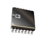
ICGOO电子元器件商城为您提供AD8302ARUZ由Analog设计生产,在icgoo商城现货销售,并且可以通过原厂、代理商等渠道进行代购。 AD8302ARUZ价格参考¥121.33-¥169.73。AnalogAD8302ARUZ封装/规格:RF 检测器, RF Detector IC General Purpose 2.7GHz -60dBm ~ 0dBm ±0.5dB 14-TSSOP (0.173", 4.40mm Width)。您可以下载AD8302ARUZ参考资料、Datasheet数据手册功能说明书,资料中有AD8302ARUZ 详细功能的应用电路图电压和使用方法及教程。
AD8302ARUZ是Analog Devices Inc.生产的一款高精度RF(射频)检测器,主要用于测量信号的幅度和相位差。其典型应用场景包括无线通信系统、射频功率控制、天线校准、雷达系统以及测试与测量设备。

在无线基站中,AD8302ARUZ可用于实时监测发射和接收信号的功率电平,实现自动增益控制(AGC),确保信号稳定传输。在射频收发模块中,它能够精确测量两个高频信号之间的幅度比和相位差,适用于I/Q信号平衡校正和反馈环路设计。此外,在相控阵天线系统中,该器件可用于相位一致性检测与调整,提升波束成形精度。

AD8302ARUZ工作频率范围宽(从低频至2.7 GHz),具备良好的温度稳定性与线性度,适合在复杂电磁环境中可靠运行。因其集成度高、外围电路简单,也广泛应用于便携式射频测试仪器,如场强仪、网络分析仪辅助模块等。

总之,AD8302ARUZ凭借其高精度、宽带宽和易用性,成为现代射频系统中实现信号动态监测与控制的关键元件。
| 参数 | 数值 |
| 产品目录 | |
| 描述 | IC DETECT GAIN PHASE 14-TSSOP对数放大器 2.7GHz RF/IF GAIN PHASE DETECTOR |
| DevelopmentKit | AD8302-EVALZ |
| 产品分类 | |
| 品牌 | Analog Devices |
| 产品手册 | |
| 产品图片 |
|
| rohs | 符合RoHS无铅 / 符合限制有害物质指令(RoHS)规范要求 |
| 产品系列 | 放大器 IC,对数放大器,Analog Devices AD8302ARUZ- |
| 数据手册 | |
| 产品型号 | AD8302ARUZ |
| RF类型 | 通用 |
| 产品 | Logarithmic Amplifiers |
| 产品培训模块 | http://www.digikey.cn/PTM/IndividualPTM.page?site=cn&lang=zhs&ptm=25139 |
| 产品目录页面 | |
| 产品种类 | 对数放大器 |
| 包装 | 管件 |
| 可用增益调整 | 30 dB |
| 商标 | Analog Devices |
| 安装风格 | SMD/SMT |
| 封装 | Tube |
| 封装/外壳 | 14-TSSOP(0.173",4.40mm 宽) |
| 封装/箱体 | TSSOP-14 |
| 工作温度范围 | - 40 C to + 85 C |
| 工作电源电压 | 2.7 V to 5.5 V |
| 工厂包装数量 | 96 |
| 带宽 | 30 MHz |
| 放大器类型 | Logarithmic |
| 最小工作温度 | - 40 C |
| 标准包装 | 1 |
| 电压-电源 | 2.7 V ~ 5.5 V |
| 电流-电源 | 23mA |
| 电源电流 | 19 mA |
| 类型 | Dual Channel Detector |
| 精度 | 0.5dB |
| 系列 | AD8302 |
| 视频文件 | http://www.digikey.cn/classic/video.aspx?PlayerID=1364138032001&width=640&height=505&videoID=2245193150001 |
| 输入电压范围—最大 | 5.5 V |
| 输入范围 | -60dBm ~ 0dBm |
| 通道数量 | 2 Channel |
| 频率 | 2.7GHz |


- 商务部:美国ITC正式对集成电路等产品启动337调查
- 曝三星4nm工艺存在良率问题 高通将骁龙8 Gen1或转产台积电
- 太阳诱电将投资9.5亿元在常州建新厂生产MLCC 预计2023年完工
- 英特尔发布欧洲新工厂建设计划 深化IDM 2.0 战略
- 台积电先进制程称霸业界 有大客户加持明年业绩稳了
- 达到5530亿美元!SIA预计今年全球半导体销售额将创下新高
- 英特尔拟将自动驾驶子公司Mobileye上市 估值或超500亿美元
- 三星加码芯片和SET,合并消费电子和移动部门,撤换高东真等 CEO
- 三星电子宣布重大人事变动 还合并消费电子和移动部门
- 海关总署:前11个月进口集成电路产品价值2.52万亿元 增长14.8%


PDF Datasheet 数据手册内容提取
a LF–2.7 GHz RF/IF Gain and Phase Detector AD8302 FEATURES FUNCTIONAL BLOCK DIAGRAM Measures Gain/Loss and Phase up to 2.7 GHz Dual Demodulating Log Amps and Phase Detector AD8302 Input Range –60 dBm to 0 dBm in a 50 (cid:1) System MFLT VIDEO OUTPUT – A + + Accurate Gain Measurement Scaling (30 mV/dB) VMAG Typical Nonlinearity < 0.5 dB INPA 60dB LOG AMPS – – Accurate Phase Measurement Scaling (10 mV/Degree) OFSA (7 DETECTORS) Typical Nonlinearity < 1 Degree Measurement/Controller/Level Comparator Modes MSET Operates from Supply Voltages of 2.7 V–5.5 V COMM PHASE Stable 1.8 V Reference Voltage Output DETECTOR PSET Small Signal Envelope Bandwidth from DC to 30 MHz APPLICATIONS OFSB 60dB LOG AMPS – RF/IF PA Linearization INPB (7 DETECTORS) VPHS + Precise RF Power Control VIDEO OUTPUT – B PFLT Remote System Monitoring and Diagnostics 1.8V Return Loss/VSWR Measurements VPOS BIAS x3 VREF Log Ratio Function for AC Signals PRODUCT DESCRIPTION The signal inputs are single-ended, allowing them to be matched The AD8302 is a fully integrated system for measuring gain/loss and connected directly to a directional coupler. Their input and phase in numerous receive, transmit, and instrumentation impedance is nominally 3 kΩ at low frequencies. applications. It requires few external components and a single The AD8302 includes a phase detector of the multiplier type, supply of 2.7 V–5.5 V. The ac-coupled input signals can range but with precise phase balance driven by the fully limited signals from –60 dBm to 0 dBm in a 50 Ω system, from low frequencies appearing at the outputs of the two logarithmic amplifiers. up to 2.7 GHz. The outputs provide an accurate measurement Thus, the phase accuracy measurement is independent of signal of either gain or loss over a ±30 dB range scaled to 30 mV/dB, level over a wide range. and of phase over a 0°–180° range scaled to 10 mV/degree. Both subsystems have an output bandwidth of 30 MHz, which The phase and gain output voltages are simultaneously available at loadable ground referenced outputs over the standard output may optionally be reduced by the addition of external filter range of 0 V to 1.8 V. The output drivers can source or sink up capacitors. The AD8302 can be used in controller mode to to 8 mA. A loadable, stable reference voltage of 1.8 V is avail- force the gain and phase of a signal chain toward predetermined able for precise repositioning of the output range by the user. setpoints. In controller applications, the connection between the gain The AD8302 comprises a closely matched pair of demodulating output pin VMAG and the setpoint control pin MSET is broken. logarithmic amplifiers, each having a 60 dB measurement range. The desired setpoint is presented to MSET and the VMAG By taking the difference of their outputs, a measurement of control signal drives an appropriate external variable gain device. the magnitude ratio or gain between the two input signals is Likewise, the feedback path between the phase output pin VPHS available. These signals may even be at different frequencies, and its setpoint control pin PSET may be broken to allow allowing the measurement of conversion gain or loss. The AD8302 operation as a phase controller. may be used to determine absolute signal level by applying the unknown signal to one input and a calibrated ac reference signal The AD8302 is fabricated on Analog Devices’ proprietary, high to the other. With the output stage feedback connection dis- performance 25 GHz SOI complementary bipolar IC process. It is abled, a comparator may be realized, using the setpoint pins available in a 14-lead TSSOP package and operates over a –40°C MSET and PSET to program the thresholds. to +85°C temperature range. An evaluation board is available. REV. B Document Feedback Information furnished by Analog Devices is believed to be accurate and reliable. However, no responsibility is assumed by Analog Devices for its One Technology Way, P.O. Box 9106, Norwood, MA 02062-9106, U.S.A. use, nor for any infringements of patents or other rights of third parties that may result from its use. No license is granted by implication or otherwise Tel: 781.329.4700 ©2018 Analog Devices, Inc. All rights reserved. under any patent or patent rights of Analog Devices. Technical Support www.analog.com
AD8302–SPECIFICATIONS (T = 25(cid:2)C, V = 5 V, VMAG shorted to MSET, VPHS shorted to PSET, 52.3 (cid:1) shunt A S resistors connected to INPA and INPB, for Phase measurement P = P , unless otherwise noted.) INPA INPB Parameter Conditions Min Typ Max Unit OVERALL FUNCTION Input Frequency Range >0 2700 MHz Gain Measurement Range P at INPA, P at INPB = –30 dBm ±30 dB IN IN Phase Measurement Range φ at INPA > φ at INPB ±90 Degree IN IN Reference Voltage Output Pin VREF, –40°C ≤ T ≤ +85°C 1.72 1.8 1.88 V A INPUT INTERFACE Pins INPA and INPB Input Simplified Equivalent Circuit To AC Ground, f ≤ 500 MHz 3(cid:1)2 kΩ(cid:1)pF Input Voltage Range AC-Coupled (0 dBV = 1 V rms) –73 –13 dBV re: 50 Ω –60 0 dBm Center of Input Dynamic Range –43 dBV –30 dBm MAGNITUDE OUTPUT Pin VMAG Output Voltage Minimum 20 × Log (V /V ) = –30 dB 30 mV INPA INPB Output Voltage Maximum 20 × Log (V /V ) = +30 dB 1.8 V INPA INPB Center Point of Output (MCP) V = V 900 mV INPA INPB Output Current Source/Sink 8 mA Small Signal Envelope Bandwidth Pin MFLT Open 30 MHz Slew Rate 40 dB Change, Load 20 pF(cid:1)10 kΩ 25 V/µs Response Time Rise Time Any 20 dB Change, 10%–90% 50 ns Fall Time Any 20 dB Change, 90%–10% 60 ns Settling Time Full-Scale 60 dB Change, to 1% Settling 300 ns PHASE OUTPUT Pin VPHS Output Voltage Minimum Phase Difference 180 Degrees 30 mV Output Voltage Maximum Phase Difference 0 Degrees 1.8 V Phase Center Point When φ = φ ±90° 900 mV INPA INPB Output Current Drive Source/Sink 8 mA Slew Rate 25 V/µs Small Signal Envelope Bandwidth 30 MHz Response Time Any 15 Degree Change, 10%–90% 40 ns 120 Degree Change C =1 pF, to 1% Settling 500 ns FILT 100 MHz MAGNITUDE OUTPUT Dynamic Range ±1 dB Linearity P = –30 dBm (V = –43 dBV) 58 dB REF REF ±0.5 dB Linearity P = –30 dBm (V = –43 dBV) 55 dB REF REF ±0.2 dB Linearity P = –30 dBm (V = –43 dBV) 42 dB REF REF Slope From Linear Regression 29 mV/dB Deviation vs. Temperature Deviation from Output at 25°C –40°C ≤ T ≤ +85°C, P = P = –30 dBm 0.25 dB A INPA INPB Deviation from Best Fit Curve at 25°C –40°C ≤ T ≤ +85°C, P = ±25 dB, P = –30 dBm 0.25 dB A INPA INPB Gain Measurement Balance P = P = –5 dBm to –50 dBm 0.2 dB INPA INPB PHASE OUTPUT Dynamic Range Less than ±1 Degree Deviation from Best Fit Line 145 Degree Less than 10% Deviation in Instantaneous Slope 143 Degree Slope (Absolute Value) From Linear Regression about –90° or +90° 10 mV/Degree Deviation vs. Temperature Deviation from Output at 25°C –40°C ≤ T ≤ +85°C, Delta Phase = 90 Degrees 0.7 Degree A Deviation from Best Fit Curve at 25°C –40°C ≤ T ≤ +85°C, Delta Phase = ±30 Degrees 0.7 Degree A –2– REV. B
AD8302 Parameter Conditions Min Typ Max Unit 900 MHz MAGNITUDE OUTPUT Dynamic Range ±1 dB Linearity P = –30 dBm (V = –43 dBV) 58 dB REF REF ±0.5 dB Linearity P = –30 dBm (V = –43 dBV) 54 dB REF REF ±0.2 dB Linearity P = –30 dBm (V = –43 dBV) 42 dB REF REF Slope From Linear Regression 28.7 mV/dB Deviation vs. Temperature Deviation from Output at 25°C –40°C ≤ T ≤ +85°C, P = P = –30 dBm 0.25 dB A INPA INPB Deviation from Best Fit Curve at 25°C –40°C ≤ T ≤ +85°C, P = ±25 dB, P = –30 dBm 0.25 dB A INPA INPB Gain Measurement Balance P = P = –5 dBm to –50 dBm 0.2 dB INPA INPB PHASE OUTPUT Dynamic Range Less than ± 1 Degree Deviation from Best Fit Line 143 Degree Less than 10% Deviation in Instantaneous Slope 143 Degree Slope (Absolute Value) From Linear Regression about –90° or +90° 10.1 mV/Degree Deviation Linear Deviation from Best Fit Curve at 25°C –40°C ≤ T ≤ +85°C, Delta Phase = 90 Degrees 0.75 Degree A –40°C ≤ T ≤ +85°C, Delta Phase = ±30 Degrees 0.75 Degree A Phase Measurement Balance Phase @ INPA = Phase @ INPB, P = –5 dBm to –50 dBm 0.8 Degree IN 1900 MHz MAGNITUDE OUTPUT Dynamic Range ±1 dB Linearity P = –30 dBm (V = –43 dBV) 57 dB REF REF ±0.5 dB Linearity P = –30 dBm (V = –43 dBV) 54 dB REF REF ±0.2 dB Linearity P = –30 dBm (V = –43 dBV) 42 dB REF REF Slope From Linear Regression 27.5 mV/dB Deviation vs. Temperature Deviation from Output at 25°C –40°C ≤ T ≤ +85°C, P = P = –30 dBm 0.27 dB A INPA INPB Deviation from Best Fit Curve at 25°C –40°C ≤ T ≤ +85°C, P = ±25 dB, P = –30 dBm 0.33 dB A INPA INPB Gain Measurement Balance P = P = –5 dBm to –50 dBm 0.2 dB INPA INPB PHASE OUTPUT Dynamic Range Less than ±1 Degree Deviation from Best Fit Line 128 Degree Less than 10% Deviation in Instantaneous Slope 120 Degree Slope (Absolute Value) From Linear Regression about –90° or +90° 10.2 mV/Degree Deviation Linear Deviation from Best Fit Curve at 25°C –40°C ≤ T ≤ +85°C, Delta Phase = 90 Degrees 0.8 Degree A –40°C ≤ T ≤ +85°C, Delta Phase = ±30 Degrees 0.8 Degree A Phase Measurement Balance Phase @ INPA = Phase @ INPB, P = –5 dBm to –50 dBm 1 Degree IN 2200 MHz MAGNITUDE OUTPUT Dynamic Range ±1 dB Linearity P = –30 dBm (V = –43 dBV) 53 dB REF REF ±0.5 dB Linearity P = –30 dBm (V = –43 dBV) 51 dB REF REF ±0.2 dB Linearity P = –30 dBm (V = –43 dBV) 38 dB REF REF Slope From Linear Regression 27.5 mV/dB Deviation vs. Temperature Deviation from Output at 25°C –40°C ≤ T ≤ +85°C, P = P = –30 dBm 0.28 dB A INPA INPB Deviation from Best Fit Curve at 25°C –40°C ≤ T ≤ +85°C, P = ±25 dB, P = –30 dBm 0.4 dB A INPA INPB Gain Measurement Balance P = P = –5 dBm to –50 dBm 0.2 dB INPA INPB PHASE OUTPUT Dynamic Range Less than ±1 Degree Deviation from Best Fit Line 115 Degree Less than 10% Deviation in Instantaneous Slope 110 Degree Slope (Absolute Value) From Linear Regression about –90° or +90° 10 mV/Degree Deviation Linear Deviation from Best Fit Curve at 25°C –40°C ≤ T ≤ +85°C, Delta Phase = 90 Degrees 0.85 Degree A –40°C ≤ T ≤ +85°C, Delta Phase = ±30 Degrees 0.9 Degree A REFERENCE VOLTAGE Pin VREF Output Voltage Load = 2 kΩ 1.7 1.8 1.9 V PSRR V = 2.7 V to 5.5 V 0.25 mV/V S Output Current Source/Sink (Less than 1% Change) 5 mA POWER SUPPLY Pin VPOS Supply 2.7 5.0 5.5 V Operating Current (Quiescent) V = 5 V 19 25 mA S –40°C ≤ T ≤ +85°C 21 27 mA A Specifications subject to change without notice. REV. B –3–
AD8302 ABSOLUTE MAXIMUM RATINGS1 PIN CONFIGURATION Supply Voltage V . . . . . . . . . . . . . . . . . . . . . . . . . . . . . 5.5 V S PSET, MSET Voltage . . . . . . . . . . . . . . . . . . . . . . V + 0.3 V S INPA, INPB Maximum Input . . . . . . . . . . . . . . . . . . –3 dBV COMM 1 14 MFLT Equivalent Power Re. 50 Ω . . . . . . . . . . . . . . . . . . 10 dBm INPA 2 13 VMAG θ 2 . . . . . . . . . . . . . . . . . . . . . . . . . . . . . . . . . . . . . 150°C/W OFSA 3 AD8302 12 MSET JA Maximum Junction Temperature . . . . . . . . . . . . . . . . 125°C VPOS 4 (NToOt Pto V SIEcaWle) 11 VREF Operating Temperature Range . . . . . . . . . . . –40°C to +85°C OFSB 5 10 PSET Storage Temperature Range . . . . . . . . . . . . –65°C to +150°C INPB 6 9 VPHS Lead Temperature Range (Soldering 60 sec) . . . . . . . . 300°C COMM 7 8 PFLT NOTES 1Stresses above those listed under Absolute Maximum Ratings may cause perma- nent damage to the device. This is a stress rating only; functional operation of the device at these or any other conditions above those indicated in the operational section of this specification is not implied. Exposure to absolute maximum rating conditions for extended periods may affect device reliability. 2JEDEC 1S Standard (2-layer) board data. PIN FUNCTION DESCRIPTIONS Equivalent Pin No. Mnemonic Function Circuit 1, 7 COMM Device Common. Connect to low impedance ground. 2 INPA High Input Impedance to Channel A. Must be ac-coupled. Circuit A 3 OFSA A capacitor to ground at this pin sets the offset compensation filter corner Circuit A and provides input decoupling. 4 VPOS Voltage Supply (V ), 2.7 V to 5.5 V S 5 OFSB A capacitor to ground at this pin sets the offset compensation filter corner Circuit A and provides input decoupling. 6 INPB Input to Channel B. Same structure as INPA. Circuit A 8 PFLT Low Pass Filter Terminal for the Phase Output Circuit E 9 VPHS Single-Ended Output Proportional to the Phase Difference between INPA Circuit B and INPB. 10 PSET Feedback Pin for Scaling of VPHS Output Voltage in Measurement Mode. Circuit D Apply a setpoint voltage for controller mode. 11 VREF Internally Generated Reference Voltage (1.8 V Nominal) Circuit C 12 MSET Feedback Pin for Scaling of VMAG Output Voltage Measurement Mode. Circuit D Accepts a set point voltage in controller mode. 13 VMAG Single-Ended Output. Output voltage proportional to the decibel ratio of signals applied to INPA and INPB. Circuit B 14 MFLT Low Pass Filter Terminal for the Magnitude Output Circuit E CAUTION ESD (electrostatic discharge) sensitive device. Electrostatic charges as high as 4000 V readily WARNING! accumulate on the human body and test equipment and can discharge without detection. Although the AD8302 features proprietary ESD protection circuitry, permanent damage may occur on devices subjected to high energy electrostatic discharges. Therefore, proper ESD precautions are recommended to avoid performance degradation or loss of functionality. ESD SENSITIVE DEVICE –4– REV. B
AD8302 VPOS VPOS 100mV 4k(cid:1) INPA(INPB) 4k(cid:1) + 750(cid:1) 25(cid:1) VMAG ON TO (VPHS) OFSA(OFSB) LOG-AMP – CLASS A-B 10pF 2k(cid:1) CONTROL COMM COMM Circuit A Circuit B VPOS VPOS VPOS MFLT VREF MSET 10k(cid:1) (PFLT) 10k(cid:1) (PSET) 1.5pF 10k(cid:1) 5k(cid:1) ACTIVE LOADS COMM COMM COMM Circuit C Circuit D Circuit E Figure 1.Equivalent Circuits REV. B –5–
AD8302–Typical Performance Characteristics (V = 5 V, V is the reference input and V is swept, unless otherwise noted. All references to dBm are referred to 50 (cid:1). For the phase output S INPB INPA curves, the input signal levels are equal, unless otherwise noted.) 2.0 1.80 3.0 900 1.8 1.65 2.5 100 1.50 2.0 1.6 1.35 1.5 1.4 B 2200 1.20 1.0 – d VMAG – V110...208 2700 1900 VMAG – V100...097505 –40(cid:2)C +85(cid:2)C +25(cid:2)C 00–..050.5 OR IN VMAG 0.6 0.60 –1.0 ERR 0.45 –1.5 0.4 0.30 –2.0 0.2 0.15 –2.5 0 0 –3.0 –30 –25 –20 –15 –10 –5 0 5 10 15 20 25 30 –30 –20 –10 0 10 20 30 MAGNITUDE RATIO – dB MAGNITUDE RATIO – dB TPC 1.Magnitude Output (VMAG)vs. Input Level Ratio TPC 4.VMAG and Log Conformance vs. Input Level Ratio (Gain) V /V , Frequencies 100 MHz, 900 MHz, (Gain), Frequency 900 MHz, –40(cid:2)C, +25(cid:2)C, and +85(cid:2)C, INPA INPB 1900 MHz, 2200 MHz, 2700 MHz, 25(cid:2)C, P = –30 dBm, Reference Level = –30 dBm INPB (Re: 50 Ω) 2.0 1.80 3.0 1900 1.8 1.65 2.5 1.50 2.0 1.6 1.35 1.5 1.4 B 2700 1.20 1.0 – d VMAG – V110...208 VMAG – V100...097505 –40(cid:2)C +85(cid:2)C+25(cid:2)C 00–..050.5OR IN VMAG 0.6 2200 00..6405 ––11..05ERR 0.4 0.30 –2.0 0.2 900 0.15 –2.5 100 0 0 –3.0 –30 –25 –20 –15 –10 –5 0 5 10 15 20 25 30 –30 –20 –10 0 10 20 30 MAGNITUDE RATIO – dB MAGNITUDE RATIO – dB TPC 2.VMAG vs. Input Level Ratio (Gain) V /V , TPC 5.VMAG and Log Conformance vs. Input Level Ratio INPA INPB Frequencies 100 MHz, 900 MHz, 1900 MHz, 2200 MHz, (Gain), Frequency 1900 MHz, –40(cid:2)C, +25(cid:2)C, and +85(cid:2)C, 2700 MHz, P = –30 dBm Reference Level = –30 dBm INPA 1.80 3.0 1.80 3.0 1.65 2.5 1.65 2.5 1.50 2.0 1.50 2.0 1.35 1.5 1.35 1.5 B B VMAG – V1100....20970505 –40(cid:2)C +85(cid:2)C +25(cid:2)C 100–...0050.5 OR IN VMAG – d VMAG – V1100....20970505 –40(cid:2)C ++852(cid:2)5C(cid:2)C 100–...0050.5OR IN VMAG – d 0.60 –1.0 RR 0.60 –1.0RR E E 0.45 –1.5 0.45 –1.5 0.30 –2.0 0.30 –2.0 0.15 –2.5 0.15 –2.5 0 –3.0 0 –3.0 –30 –20 –10 0 10 20 30 –30 –20 –10 0 10 20 30 MAGNITUDE RATIO – dB MAGNITUDE RATIO – dB TPC 3.VMAG Output and Log Conformance vs. Input TPC 6.VMAG Output and Log Conformance vs. Input Level Ratio (Gain), Frequency 100 MHz, –40(cid:2)C, +25(cid:2)C, Level Ratio (Gain), Frequency 2200 MHz, –40(cid:2)C, +25(cid:2)C, and +85(cid:2)C, Reference Level = –30 dBm and +85(cid:2)C, Reference Level = –30 dBm –6– REV. B
AD8302 3.0 2.0 2.5 1.8 2.0 1.6 1.5 –40C B +85C 1.4 d 1.0 – R IN VMAG –000...505 VMAG – V 110...208 O ERR–1.0 +85C 0.6 –1.5 +25C –40C 0.4 –2.0 0.2 –2.5 –3.0 0.0 –30 –25 –20 –15 –10 –5 0 5 10 15 20 25 30 –30 –25 –20 –15 –10 –5 0 5 10 15 20 25 30 MAGNITUDE RATIO – dB MAGNITUDE RATIO – dB TPC 7.Distribution of Magnitude Error vs. Input Level TPC 10.Distribution of VMAG vs. Input Level Ratio (Gain), Ratio (Gain), Three Sigma to Either Side of Mean, Three Sigma to Either Side of Mean, Frequency 1900 MHz, Frequency 900 MHz, –40(cid:2)C, +25(cid:2)C, and +85(cid:2)C, Refer- Temperatures Between –40(cid:2)C and +85(cid:2)C, Reference Level ence Level = –30 dBm = –30 dBm 3.0 1.8 3.0 –45dBm 2.5 2.5 1.6 2.0 2.0 1.4 –45dBm –30dBm 1.5 1.5 –40C B +85C B d 1.0 1.2 1.0 d VMAG – 00..50 G – V 1.0 –15dBm 00..50 VMAG – R IN –0.5 VMA 0.8 –30dBm –0.5 R IN O –15dBm O RR–1.0 0.6 –1.0 RR E E –1.5 +25C –1.5 0.4 –40C +85C –2.0 –2.0 0.2 –2.5 –2.5 –3.0 0.0 –3.0 –30 –25 –20 –15 –10 –5 0 5 10 15 20 25 30 –30 –20 –10 0 10 20 30 MAGNITUDE RATIO – dB MAGNITUDE RATIO – dB TPC 8.Distribution of Error vs. Input Level Ratio (Gain), TPC 11.VMAG Output and Log Conformance vs. Input Three Sigma to Either Side of Mean, Frequency 1900 MHz, Level Ratio (Gain), Reference Level = –15 dBm, –30 dBm, –40(cid:2)C, +25(cid:2)C, and +85(cid:2)C, Reference Level = –30 dBm and –45 dBm, Frequency 1900 MHz 3.0 1.10 2.5 2.0 1.05 PINPA = PINPB + 5dB –40C 1.5 B +85C 1.00 d 1.0 – MAG 0.5 – V 0.95 R IN V–00..05 VMAG 0.90 PINPA = PINPB O RR–1.0 E +25C +85C 0.85 –1.5 –40C –2.0 0.80 –2.5 PINPA = PINPB – 5dB –3.0 0.75 –30 –25 –20 –15 –10 –5 0 5 10 15 20 25 30 –65 –60 –55 –50 –45 –40 –35 –30 –25 –20 –15 –10 –5 0 MAGNITUDE RATIO – dB INPUT LEVEL – dBm TPC 9.Distribution of Magnitude Error vs. Input Level TPC 12.VMAG Output vs. Input Level for P = P , INPA INPB Ratio (Gain), Three Sigma to Either Side of Mean, P = P + 5 dB, P = P – 5 dB, Frequency 1900 MHz INPA INPB INPA INPB Frequency 2200 MHz, Temperatures –40(cid:2)C, +25(cid:2)C, and +85(cid:2)C, Reference Level = –30 dBm REV. B –7–
AD8302 1.06 1.04 18 1.02 PINPA = PINPB + 5dB 1.00 15 0.98 0.96 0.94 12 MAG – V000...998208 PINPA = PINPB ERCENT 9 V P 0.86 0.84 6 0.82 0.80 3 0.78 PINPA = PINPB – 5dB 0.76 0.74 0 0 200 400 600 800 1000120014001600180020002200 0.80 0.85 0.90 0.95 1.00 FREQUENCY – MHz MCP – V TPC 13.VMAG Output vs. Frequency, for P = P , P TPC 16.Center Point of Magnitude Output (MCP) INPA INPB INPA = P + 5 dB, and P = P – 5 dB, P = –30 dBm Distribution Frequencies 900 MHz, 17,000 Units INPB INPA INPB INPB 0.4 18 0.2 0 15 V–0.2 m E – –0.4 12 E IN SLOP––00..68 PERCENT 9 ANG–1.0 6 CH–1.2 –1.4 3 –1.6 –1.8 0 –40 –20 0 20 40 60 80 85 27.0 27.5 28.0 28.5 29.0 29.5 30.0 TEMPERATURE – (cid:2)C VMAG SLOPE – mV/dB TPC 14.Change in VMAG Slope vs. Temperature, Three TPC 17.VMAG Slope, Frequency 900 MHz, 17,000 Units Sigma to Either Side of Mean, Frequencies 1900 MHz 25 0.032 20 15 0.030 10 V – mV 5 MAG G – 0 F V0.028 A O VM –5 PE O L –10 S 0.026 –15 –20 –25 0.024 –40 –30 –20 –10 0 10 20 30 40 50 60 70 80 90 0 0 0 0 0 0 0 0 0 0 0 0 0 0 0 0 0 0 0 0 0 0 0 0 0 0 0 0 0 TEMPERATURE – (cid:2)C 2 4 6 8 10 12 14 16 18 20 22 24 26 28 FREQUENCY – MHz TPC 15.Change in Center Point of Magnitude Output TPC 18.VMAG Slope vs. Frequency (MCP) vs. Temperature, Three Sigma to Either Side of Mean, Frequencies 1900 MHz –8– REV. B
AD8302 10000 INPUT –50dBm 1000 Hz V/ n INPUT –30dBm – G A M INPUT –10dBm 20mV PER V 100 VERTICAL DIVISION 25ns HORIZONTAL 10 1k 10k 100k 1M 10M 100M FREQUENCY – Hz TPC 19.Magnitude Output Response to 4 dB Step, for TPC 22.Magnitude Output Noise Spectral P = –30 dBm, P = –32 dBm to –28 dBm, Frequency Density, P = P = –10 dBm, –30 dBm, INPB INPA INPA INPB 1900 MHz, No Filter Capacitor –50 dBm, No Filter Capacitor 10000 INPUT –50dBm 1000 Hz nV/ INPUT –30dBm – 20mV PER G VERTICAL MA DIVISION V 100 INPUT –10dBm 1.00(cid:3)s HORIZONTAL 10 1k 10k 100k 1M 10M 100M FREQUENCY – Hz TPC 20.Magnitude Output Response to 4 dB Step, for TPC 23.Magnitude Output Noise Spectral Density, PINPA = PINPB P = –30 dBm, P = –32 dBm to –28 dBm, Frequency = –10 dBm, –30 dBm, –50 dBm, with Filter Capacitor, C = 1 nF INPB INPA 1900 MHz, 1 nF Filter Capacitor 0.18 0.16 0.14 V – K) 0.12 A E P O-0.10 T K- 200mV PER A0.08 VERTICAL PE 1900 2700 DIVISION G (0.06 A 2200 M 900 V0.04 100ns 100 HORIZONTAL 0.02 0.00 –25 –20 –15 –10 –5 0 5 10 15 20 25 MAGNITUDE RATIO – dB TPC 21.Magnitude Output Response to 40 dB Step, for TPC 24.VMAG Peak-to-Peak Output Induced by Sweeping P = –30 dBm, P = –50 dBm to –10 dBm, Supply 5 V, Phase Difference through 360 Degrees vs. Magnitude Ratio, INPB INPA Frequency 1900 MHz, No Filter Capacitor Frequencies 100 MHz, 900 MHz, 1900 MHz, 2200 MHz, and 2700 MHz REV. B –9–
AD8302 1.8 1.80 10 1.6 100MHz 900MHz 1.62 8 1.44 6 1.4 1900MHz 1.26 4 1.2 s HASE OUT – V10..08 2200MH2z700MHz HASE OUT – V100...097802 –202ROR – Degree P0.6 P ER 0.54 –4 0.4 0.36 –6 0.2 0.18 –8 0.0 0.00 –10 –180 –140 –100 –60 –20 20 60 100 140 180 –180–150–120 –90 –60 –30 0 30 60 90 120 150 180 PHASE DIFFERENCE – Degrees PHASE DIFFERENCE – Degrees TPC 25.Phase Output (VPHS) vs. Input Phase Difference, TPC 28.VPHS Output and Nonlinearity vs. Input Phase Input Levels –30 dBm, Frequencies 100 MHz, 900 MHz, Difference, Input Levels –30 dBm, Frequency 1900 MHz 1900 MHz, 2200 MHz, Supply 5 V, 2700 MHz 1.80 10 1.80 10 1.62 8 1.62 8 1.44 6 1.44 6 1.26 4 1.26 4 s s HASE OUT – V100...097802 –202ROR – Degree HASE OUT – V 100...097802 –202ROR – Degree P R P R E E 0.54 –4 0.54 –4 0.36 –6 0.36 –6 0.18 –8 0.18 –8 0.00 –10 0.00 –10 –180–150–120 –90 –60 –30 0 30 60 90 120 150 180 –180–150–120 –90 –60 –30 0 30 60 90 120 150 180 PHASE DIFFERENCE – Degrees PHASE DIFFERENCE – Degrees TPC 26.VPHS Output and Nonlinearity vs. Input Phase TPC 29.VPHS Output and Nonlinearity vs. Input Phase Difference, Input Levels –30 dBm, Frequency 100 MHz Difference, Input Levels –30 dBm, Frequency 2200 MHz 1.80 10 10 1.62 8 8 1.44 6 6 1.26 4 4 V es es +25(cid:2)C HASE OUT – 100...097802 –202ROR – Degre ROR – Degre–220 P ER ER +85(cid:2)C 0.54 –4 –4 –40(cid:2)C 0.36 –6 –6 0.18 –8 –8 0.00 –10 –10 –180–150–120 –90 –60 –30 0 30 60 90 120 150 180 –180–150–120 –90 –60 –30 0 30 60 90 120 150 180 PHASE DIFFERENCE – Degrees PHASE DIFFERENCE – Degrees TPC 27.VPHS Output and Nonlinearity vs. Input Phase TPC 30.Distribution of VPHS Error vs. Input Phase Differ- Difference, Input Levels –30 dBm, Frequency 900 MHz ence, Three Sigma to Either Side of Mean, Frequency 900 MHz, –40(cid:2)C, +25(cid:2)C, and +85(cid:2)C, Input Levels –30 dBm –10– REV. B
AD8302 10 0.15 8 0.10 6 V 0.05 MEAN +3 SIGMA m Degrees 42 +25(cid:2)C –40(cid:2)C S SLOPE – –00..0050 R – 0 VPH –0.10 ERRO––24 +85(cid:2)C NGE IN ––00..2105 MEAN –3 SIGMA A H –6 C –0.25 –8 –0.30 –10 –0.35 –180–150–120 –90 –60 –30 0 30 60 90 120 150 180 –40 –30 –20 –10 0 10 20 30 40 50 60 70 80 90 PHASE DIFFERENCE – Degrees TEMPERATURE – (cid:2)C TPC 31.Distribution of VPHS Error vs. Input Phase TPC 34.Change in VPHS Slope vs. Temperature, Three Difference, Three Sigma to Either Side of Mean, Frequency Sigma to Either Side of Mean, Frequency 1900 MHz 1900 MHz, –40(cid:2)C, +25(cid:2)C, and +85(cid:2)C, Supply 5 V, Input Levels P = P = –30 dBm INPA INPB 10 10 +3 SIGMA 8 5 6 0 s 4 +85(cid:2)C +25(cid:2)C –5 e – Degre 20 CENT ––1150 –3 SIGMA R R RO–2 PE –20 R E –4 –25 –40(cid:2)C –6 –30 –8 –35 –10 –40 –180–150–120 –90 –60 –30 0 30 60 90 120 150 180 –40 –30 –20 –10 0 10 20 30 40 50 60 70 80 90 PHASE DIFFERENCE – Degrees VPHS – mV/Degree TPC 32.Distribution of VPHS Error vs. Input Phase Differ- TPC 35.Change in Phase Center Point (PCP) vs. ence, Three Sigma to Either Side of Mean, Frequency Temperature, Three Sigma to Either Side of Mean, 2200 MHz, –40(cid:2)C, +25(cid:2)C, and +85(cid:2)C, Input Levels –30 dBm Frequency 1900MHz 1.8 18 1.6 15 1.4 1.2 12 S – V1.0 CENT 9 VPH0.8 PER 0.6 6 0.4 3 0.2 0.0 0 –180–150–120 –90 –60 –30 0 30 60 90 120 150 180 0.75 0.80 0.85 0.90 0.95 1.00 1.05 PHASE DIFFERENCE – Degrees PCP – V TPC 33.Distribution of VPHS vs. Input Phase Differ- TPC 36.Phase Center Point (PCP) Distribution, Frequency ence, Three Sigma to Either Side of Mean, Frequency 900 MHz, 17,000 Units 900 MHz, Temperature between –40(cid:2)C and +85(cid:2)C, Input Levels –30 dBm REV. B –11–
AD8302 16 14 12 10 T 100mV PER N RCE 8 VDEIVRISTIIOCANL E P 6 4 2 50ns HORIZONTAL 0 9.5 9.7 9.9 10.1 10.3 10.5 10.7 10.9 11.1 VPHS – mV/Degree TPC 37.VPHS Slope Distribution, Frequency TPC 40.VPHS Output Response to 40(cid:2) Step with Nominal 900 MHz Phase Shift of 90(cid:2), Input Levels P = P = –30 dBm, INPA INPB Frequency 1900 MHz,1 pF Filter Capacitor 10000 INPUT –50dBm 1000 Hz INPUT –30dBm 1VD0EIVmRISVTII OCPEANRL – nV/ INPUT –10dBm S H P V 100 50ns HORIZONTAL 10 1k 10k 100k 1M 10M 100M FREQUENCY – Hz TPC 38.VPHS Output Response to 4(cid:2) Step with Nominal TPC 41.VPHS Output Noise Spectral Density vs. Frequency, Phase Shift of 90(cid:2), Input Levels –30 dBm, Frequency P = –30 dBm, P = –10 dBm, –30 dBm, –50 dBm, and INPA INPB 1900 MHz, 25(cid:2)C, 1 pF Filter Capacitor 90(cid:2) Input Phase Difference 1.80 PINPA = –30dBm 1.62 1.44 PINPA = –15dBm 1.26 V – 1.08 10mV PER UT PINPA = –45dBm VERTICAL O0.90 DIVISION E S A0.72 H P 0.54 0.36 2(cid:3)s HORIZONTAL 0.18 0.00 –180–150–120 –90 –60 –30 0 30 60 90 120 150 180 PHASE DIFFERENCE – Degrees TPC 39.VPHS Output Response to 4(cid:2) Step with Nominal TPC 42.Phase Output vs. Input Phase Difference, P = INPA Phase Shift of 90(cid:2), Input Levels PINPA = PINPB = –30 dBm, PINPB, PINPA = PINPB + 15 dB, PINPA = PINPB – 15 dB, Frequency Supply 5 V, Frequency 1900 MHz, 25(cid:2)C, with 100 pF Filter 900 MHz Capacitor –12– REV. B
AD8302 12 1.80 PINPA = –15dBm PINPA = –30dBm PINPA = –20dBm 1.62 10 V 1.44 Sm ABSOLUTE VALUE OF VPHINSTANTANEOUS SLOPE – 8642 PINPA = –45dBm PHASE OUT – V 110000......209753680246 PINPA = –40dBm 0.18 PINPA = –30dBm 0 0.00 –180–150–120 –90 –60 –30 0 30 60 90 120 150 180 –180–150–120 –90 –60 –30 0 30 60 90 120 150 180 PHASE DIFFERENCE – Degrees PHASE DIFFERENCE – Degrees TPC 43.Phase Output Instantaneous Slope, TPC 46.Phase Output vs. Input Phase Difference, P = P , P = P + 15 dB, P = P – 15 dB, P = P , P = P + 10 dB, P = P – 10 dB, INPA INPB INPA INPB INPA INPB INPA INPB INPA INPB INPA INPB Frequency 900 MHz Frequency 2200 MHz 1.80 12 PINPA = –20dBm PINPA = –20dBm 1.62 10 1.44 V E OUT – V110...209680 PINPA = –40dBm VALUE OF VPHSOUS SLOPE – m 86 PINPA = –30dBm PINPA = –40dBm HAS0.72 UTE ANE P00..5346 PINPA = –30dBm ABSOLINSTANT 4 2 0.18 0.00 0 –180–150–120 –90 –60 –30 0 30 60 90 120 150 180 –180–150–120 –90 –60 –30 0 30 60 90 120 150 180 PHASE DIFFERENCE – Degrees PHASE DIFFERENCE – Degrees TPC 44.Phase Output vs. Input Phase Difference, TPC 47.Phase Output Instantaneous Slope, PINPA = PINPB, P = P , P = P + 10 dB, P = P – 10 dB, P = P + 10 dB, P = P – 10 dB, Frequency INPA INPB INPA INPB INPA INPB INPA INPB INPA INPB Frequency 1900 MHz, Supply 5 V 2200 MHz 12 4000 4.0 3500 3.5 10 V OLUTE VALUE OF VPHSNTANEOUS SLOPE – m 864 PINPAP IN= P–A3 =0 d–B4m0dBm (cid:1)RESISTANCE – 3221050500000000 SHURNETA CL SHSUHNUTN TZ R((cid:1)) 3221....0505 CAPACITANCE – pF ABSNSTA 1000 1.0 I 2 CAPACITANCE SHUNT Z (pF) 500 0.5 PINPA = –20dBm 0 0 0.0 –180–150–120 –90 –60 –30 0 30 60 90 120 150 180 0 500 1000 1500 2000 2500 PHASE DIFFERENCE – Degrees FREQUENCY – MHz TPC 45.Phase Output Instantaneous Slope, P = TPC 48.Input Impedance, Modeled as Shunt R in Parallel INPA P , P = P + 10 dB, P = P – 10 dB, with Shunt C INPB INPA INPB INPA INPB Frequency 1900 MHz, Supply 5 V REV. B –13–
AD8302 8 18 6 15 4 12 mV 2 NT EF – RCE 9 R 0 E V P 6 –2 3 –4 –6 0 –40 –30 –20 –10 0 10 20 30 40 50 60 70 80 90 1.74 1.76 1.78 1.80 1.82 1.84 1.86 1.88 TEMPERATURE – (cid:2)C VREF – V TPC 49.Change in VREF vs. Temperature, Three Sigma to TPC 51.VREF Distribution, 17,000 Units Either Side of Mean 120 100 80 Hz V/ n – 60 E S OI N 40 20 0 1k 10k 100k 1M 10M 100M FREQUENCY – Hz TPC 50.VREF Output Noise Spectral Density vs. Frequency –14– REV. B
AD8302 GENERAL DESCRIPTION AND THEORY [ ( ) ( )] The AD8302 measures the magnitude ratio, defined here as V PHS =VΦ ΦVINA −ΦVINB (3) gain, and phase difference between two signals. A pair of where VΦ is the phase slope in mV/degree and Φ is each signal’s matched logarithmic amplifiers provide the measurement, and relative phase in degrees. their hard-limited outputs drive the phase detector. Structure Basic Theory The general form of the AD8302 is shown in Figure 2. The Logarithmic amplifiers (log amps) provide a logarithmic com- major blocks consist of two demodulating log amps, a phase pression function that converts a large range of input signal detector, output amplifiers, a biasing cell, and an output refer- levels to a compact decibel-scaled output. The general math- ence voltage buffer. The log amps and phase detector process ematical form is: the high frequency signals and deliver the gain and phase infor- ( ) mation in current form to the output amplifiers. The output V =V logV /V (1) OUT SLP IN Z amplifiers determine the final gain and phase scaling. External filter capacitors set the averaging time constants for the respec- where V is the input voltage, V is called the intercept (voltage), IN Z tive outputs. The reference buffer provides a 1.80 V reference and V is called the slope (voltage). It is assumed throughout SLP that log(x) represents the log10(x) function. V is thus the voltage that tracks the internal scaling constants. SLP volts/decade, and since a decade of voltage corresponds to 20 dB, VSLP/20 is the volts/dB. VZ is the value of input VIDEO OUTPUT – A + + MFLT signal that results in an output of zero and need not correspond VMAG – – to a physically realizable part of the log amp signal range. INPA 60dB LOG AMPS OFSA (7 DETECTORS) While the slope is fundamentally a characteristic of the log amp, the intercept is a function of the input waveform as well.1 MSET Furthermore, the intercept is typically more sensitive to tem- perature and frequency than the slope. When single log amps COMM PHASE DETECTOR are used for power measurement, this variability introduces PSET errors into the absolute accuracy of the measurement since the intercept represents a reference level. The AD8302 takes the difference in the output of two identical OFSB 60dB LOG AMPS – INPB (7 DETECTORS) VPHS log amps, each driven by signals of similar waveforms but at + different levels. Since subtraction in the logarithmic domain VIDEO OUTPUT – B PFLT corresponds to a ratio in the linear domain, the resulting VPOS BIAS x3 VREF 1.8V output becomes: ( ) Figure 2.General Structure V =V logV /V (2) MAG SLP INA INB Each log amp consists of a cascade of six 10 dB gain stages with where V and V are the input voltages, V is the output seven associated detectors. The individual gain stages have 3 dB INA INB MAG corresponding to the magnitude of the signal level difference, bandwidths in excess of 5 GHz. The signal path is fully differen- and V is the slope. Note that the intercept, V , has dropped tial to minimize the effect of common-mode signals and noise. SLP Z out. Unlike the measurement of power, when measuring a dimen- Since there is a total of 60 dB of cascaded gain, slight dc offsets sionless quantity such as relative signal level, no independent can cause limiting of the latter stages, which may cause mea- reference or intercept need be invoked. In essence, one signal surement errors for small signals. This is corrected by a feedback serves as the intercept for the other. Variations in intercept due loop. The nominal high-pass corner frequency, fHP, of this loop to frequency, process, temperature, and supply voltage affect both is set internally at 200 MHz but can be lowered by adding external channels identically and hence do not affect the difference. This capacitance to the OFSA and OFSB pins. Signals at frequencies technique depends on the two log amps being well matched well below the high-pass corner are indistinguishable from dc in slope and intercept to ensure cancellation. This is the case offsets and are also nulled. The difference in the log amp out- for an integrated pair of log amps. Note that if the two signals puts is performed in the current domain, yielding by analogy to have different waveforms (e.g., different peak-to-average ratios) Equation 2: or different frequencies, an intercept difference may appear, intro- I =I log(V /V ) (4) ducing a systematic offset. LA SLP INA INB where I and I are the output current difference and the The log amp structure consists of a cascade of linear/limiting LA SLP characteristic slope (current) of the log amps, respectively. The gain stages with demodulating detectors. Further details about slope is derived from an accurate reference designed to be insen- the structure and function of log amps can be found in data sitive to temperature and supply voltage. sheets for other log amps produced by Analog Devices.2 The output of the final stage of a log amp is a fully limited signal The phase detector uses a fully symmetric structure with respect over most of the input dynamic range. The limited outputs from to its two inputs to maintain balanced delays along both signal both log amps drive an exclusive-OR style digital phase detector. paths. Fully differential signaling again minimizes the sensitivity Operating strictly on the relative zero-crossings of the limited sig- to common-mode perturbations. The current-mode equivalent nals, the extracted phase difference is independent of the original to Equation 3 is: input signal levels. The phase output has the general form: [ ( ) ( ) ] I PD =IΦ ΦVINA −ΦVINB −90° (5) NOTES 1See the data sheet for the AD640 for a description of the effect of waveform on where IPD and IΦ are the output current and characteristic slope the intercept of log amps. associated with the phase detector, respectively. The slope is 2For example, see the data sheet for the AD8307. derived from the same reference as the log amp slope. REV. B –15–
AD8302 Note that by convention, the phase difference is taken in the range VP from –180° to +180°. Since this style of phase detector does not C7 distinguish between ±90°, it is considered to have an unambiguous AD8302 R4 180° phase difference range that can be either 0° to +180° centered 1 COMM MFLT 14 at +90° or 0° to –180° centered at –90°. VINA C1 2 INPA VMAG 13 VMAG C2 The basic structure of both output interfaces is shown in Figure 3. It R1 3 OFSA MSET 12 accepts a setpoint input and includes an internal integrating/averag- C4 ing capacitor and a buffer amplifier with gain K. External access to 4 VPOS VREF 11 C6 these setpoints provides for several modes of operation and enables 5 OFSB PSET 10 flexible tailoring of the gain and phase transfer characteristics. The R2 setpoint interface block, characterized by a transresistance R , gener- VINB 6 INPB VPHS 9 VPHS F C5 ates a current proportional to the voltage presented to its input pin, 7 COMM PFLT 8 MSET or PSET. A precise offset voltage of 900 mV is introduced C3 C8 internally to establish the center-point (V ) for the gain and phase CP Figure 4.Basic Connections in Measurement Mode with functions, i.e., the setpoint voltage that corresponds to a gain of 0 dB 30 mV/dB and 10 mV/Degree Scaling and a phase difference of 90°. This setpoint current is subtracted from the signal current, I , coming from the log amps in the gain In the low frequency limit, the gain and phase transfer functions IN channel or from the phase detector in the phase channel. The result- given in Equations 4 and 5 become: ing difference is integrated on the averaging capacitors at either pin ( ) V =R I logV /V +V or (8a) MFLT or PFLT and then buffered by the output amplifier to the MAG F SLP INA INB CP respective output pins, VMAG and VPHS. With this open-loop ( )( ) V = R I /20 P −P +V (8b) arrangement, the output voltage is a simple integration of the differ- MAG F SLP INA INB CP ence between the( measured )ga(in/p)hase and the desired setpoint: V PHS =–RFIΦ(|Φ(VINA)−Φ(VINB)|–90°)+VCP (9) V =R I −I / sT (6) OUT F IN FB which are illustrated in Figure 5. In Equation 8b, PINA and PINB are the power in dBm equivalent to V and V at a specified refer- where I is the feedback current equal to (V – V )/R , V INA INB FB SET CP F SET ence impedance. For the gain function, the slope represented by is the setpoint input, and T is the integration time constant equal R I is 600 mV/decade or, dividing by 20 dB/decade, 30 mV/dB. to R C /K, where C is the parallel combination of the inter- F SLP F AVE AVE With a center point of 900 mV for 0 dB gain, a range of –30 dB to nal 1.5 pF and the external capacitor C . FLT +30 dB covers the full-scale swing from 0 V to 1.8 V. For the phase function, the slope represented by RFIΦ is 10 mV/degree. With a 1.5pF center point of 900 mV for 90°, a range of 0° to 180° covers the MFLT/PFLT full-scale swing from 1.8 V to 0 V. The range of 0° to –180° covers IIN = ILA OR IPD + K VMAG/VPHS CFLT the same full-scale swing but with the opposite slope. – IFB VCP = 900mV 1.8V + RF + MSET/PSET 20k(cid:1) 30mV/dB G Figure 3.Simplified Block Diagram of the Output Interface VMA900mV VCP BASIC CONNECTIONS Measurement Mode The basic function of the AD8302 is the direct measurement of gain and phase. When the output pins, VMAG and VPHS, are connected 0V directly to the feedback setpoint input pins, MSET and PSET, the –30 0 +30 default slopes and center points are invoked. This basic connection MAGNITUDE RATIO – dB shown in Figure 4 is termed the measurement mode. The current 1.8V from the setpoint interface is forced by the integrator to be equal to the signal currents coming from the log amps and phase detector. The closed loop transfer function is thus given by: +10mV/DEG –10mV/DEG ( ) ( ) V OUT = IINRF +VCP / 1+sT (7) PHS V 900mV VCP The time constant T represents the single-pole response to the enve- lope of the dB-scaled gain and the degree-scaled phase functions. A small internal capacitor sets the maximum envelope bandwidth to approximately 30 MHz. If no external C is used, the AD8302 FLT can follow the gain and phase envelopes within this bandwidth. If 0V longer averaging is desired, CFLT can be added as necessary accord- –180 –90 0 90 180 ing to T (ns) = 3.3 × CAVE (pF). For best transient response with PHASE DIFFERENCE – Degrees minimal overshoot, it is recommended that 1 pF minimum value Figure 5.Idealized Transfer Characteristics for the Gain external capacitors be added to the MFLT and PFLT pins. and Phase Measurement Mode –16– REV. B
AD8302 Interfacing to the Input Channels Dynamic Range The single-ended input interfaces for both channels are identical. The maximum measurement range for the gain subsystem is lim- Each consists of a driving pin, INPA and INPB, and an ac- ited to a total of 60 dB distributed from –30 dB to +30 dB. This grounding pin, OFSA and OFSB. All four pins are internally means that both gain and attenuation can be measured. The limits dc-biased at about 100 mV from the positive supply and should are determined by the minimum and maximum levels that each be externally ac-coupled to the input signals and to ground. For individual log amp can detect. In the AD8302, each log amp can the signal pins, the coupling capacitor should offer negligible detect inputs ranging from –73 dBV [(223 µV, –60 dBm re: 50 Ω impedance at the signal frequency. For the grounding pins, the to –13 dBV (223 mV, 0 dBm re: 50 Ω)]. Note that log coupling capacitor has two functions: It provides ac grounding amps respond to voltages and not power. An equivalent power and sets the high-pass corner frequency for the internal offset can be inferred given an impedance level, e.g., to convert from compensation loop. There is an internal 10 pF capacitor to ground dBV to dBm in a 50 Ω system, simply add 13 dB. To cover that sets the maximum corner to approximately 200 MHz. the entire range, it is necessary to apply a reference level to one log The corner can be lowered according the formula f (MHz) = amp that corresponds precisely to its midrange. In the AD8302, HP 2/C (nF), where C is the total capacitance from OFSA or OFSB this level is at –43 dBV, which corresponds to –30 dBm in a 50 Ω C C to ground, including the internal 10 pF. environment. The other channel can now sweep from its low end, 30 dB below midrange, to its high end, 30 dB above midrange. If The input impedance to INPA and INPB is a function of the reference is displaced from midrange, some measurement frequency, the offset compensation capacitor, and package range will be lost at the extremes. This can occur either if the log parasitics. At moderate frequencies above f , the input network can be approximated by a shunt 3 kΩ resistHoPr in parallel with a amps run out of range or if the rails at ground or 1.8 V are reached. Figure 7 illustrates the effect of the reference channel level placement. 2 pF capacitor. At higher frequencies, the shunt resistance decreases to approximately 500 Ω. The Smith Chart in Figure 6 If the reference is chosen lower than midrange by 10 dB, then the lower limit will be at –20 dB rather than –30 dB. If the reference chosen shows the input impedance over the frequency range 100 MHz is higher by 10 dB, the upper limit will be 20 dB rather than 30 dB. to 3 GHz. MAX RANGE FOR VREF = VREFOPT 1.80 V 100MHz – G A M 900MHz V 0.90 VREF < VREFOPT VREF > VREFOPT 1.8GHz 2.2GHz 2.7GHz 3.0GHz –30 0 +30 GAIN MEASUREMENT RANGE – dB Figure 6.Smith Chart Showing the Input Impedance of a Single Channel from 100 MHz to 3 GHz Figure 7.The Effect of Offsetting the Reference Level Is to Reduce the Maximum Dynamic Range A broadband resistive termination on the signal side of the coupling capacitors can be used to match to a given source impedance. The phase measurement range is of 0° to 180°. For phase differ- The value of the termination resistor, R , is determined by: ences of 0° to –180°, the transfer characteristics are mirrored as T shown in Figure 5, with a slope of the opposite sign. The phase ( ) R =R R / R −R (10) detector responds to the relative position of the zero crossings T IN S IN S between the two input channels. At higher frequencies, the finite where R is the input resistance and R the source impedance. IN S rise and fall times of the amplitude limited inputs create an At higher frequencies, a reactive, narrow-band match might be ambiguous situation that leads to inaccessible dead zones at the desirable to tune out the reactive portion of the input impedance. 0° and 180° limits. For maximum phase difference coverage, the An important attribute of the two-log-amp architecture is that if reference phase difference should be set to 90°. both channels are at the same frequency and have the same input network, then impedance mismatches and reflection losses become essentially common-mode and hence do not impact the relative gain and phase measurement. However, mismatches in these external components can result in measurement errors. REV. B –17–
AD8302 Cross Modulation of Magnitude and Phase reference that determines the nominal center point, their At high frequencies, unintentional cross coupling between signals tracking with temperature, supply, and part-to-part variations in Channels A and B inevitably occurs due to on-chip and board- should be better in comparison to a fixed external voltage. If the level parasitics. When the two signals presented to the AD8302 center point is shifted to 0 dB in the previous example where inputs are at very different levels, the cross coupling introduces the slope was doubled, then the range spans from –15 dB at cross modulation of the phase and magnitude responses. If the two V = 0 V to 15 dB at V = 1.8 V. MAG MAG signals are held at the same relative levels and the phase between them is modulated then only the phase output should respond. Due to phase-to-amplitude cross modulation, the magnitude out- NEW SLOPE = 30mV/dB (cid:4) 1(cid:5) 10Rk1(cid:1) put shows a residual response. A similar effect occurs when the VMAG relative phase is held constant while the magnitude difference is R1 MSET modulated, i.e., an expected magnitude response and a residual phase response are observed due to amplitude-to-phase cross 20k(cid:1) 20k(cid:1) modulation. The point where these effects are noticeable depends VREF on the signal frequency and the magnitude of the difference. Typi- cally, for differences <20 dB, the effects of cross modulation are negligible at 900 MHz. Figure 9.The Center Point Is Repositioned with the Help of the Internal Reference Voltage of 1.80 V Modifying the Slope and Center Point The default slope and center point values can be modified with Comparator and Controller Modes the addition of external resistors. Since the output interface The AD8302 can also operate in a comparator mode if used in blocks are generalized for both magnitude and phase functions, the arrangement shown in Figure 10 where the DUT is the element the scaling modification techniques are equally valid for both to be evaluated. The VMAG and VPHS pins are no longer outputs. Figure 8 demonstrates how a simple voltage divider connected to MSET and PSET. The trip-point thresholds for the from the VMAG and VPHS pins to the MSET and PSET pins gain and phase difference comparison are determined by the can be used to modify the slope. The increase in slope is given by voltages applied to pins MSET and PSET according to: 1 + R1/(R2(cid:1)20 kΩ). Note that it may be necessary to account for the MSET and PSET input impedance of 20 kΩ which has a ±20% V MSET(V)=30mV/dB×GainSP(dB)+900mV (11) manufacturing tolerance. As is generally true in such feedback ( ) systems, envelope bandwidth is decreased and the output noise VPSET(V)=−10mV/°× |PhaseSP(°)|–90° +900mV (12) transferred from the input is increased by the same factor. For where GainSP (dB) and PhaseSP (°) are the desired gain and example, by selecting R1 and R2 to be 10 kΩ and 20 kΩ, phase thresholds. If the actual gain and phase between the two respectively, gain slope increases from the nominal 30 mV/dB input channels differ from these thresholds, the V and V by a factor of 2 to 60 mV/dB. The range is reduced by a factor MAG PHS outputs toggle like comparators, i.e., of 2 and the new center point is at –15 dB, i.e., the range now extends from –30 dB, corresponding to V = 0 V, to 0 dB, MAG 1.8V if Gain>GainSP corresponding to VMAG = 1.8 V. V = (13) MAG 0V if Gain<GainSP 1.8V if Phase>PhaseSP VMAG NEW SLOPE = 30mV/dB (cid:4) 1(cid:5)R2||RR210k(cid:1) VPHS = 0V if Phase<PhaseSP (14) R1 MSET 20k(cid:1) R2 VP Figure 8.Increasing the Slope Requires the Inclusion of a C7 AD8302 Voltage Divider R4 1 COMM MFLT 14 Repositioning the center point back to its original value of 0 dB C1 C2 simply requires that an appropriate voltage be applied to the VINA 2 INPA VMAG 13 VMAG R1 grounded side of the lower resistor in the voltage divider. This 3 OFSA MSET 12 VMSET voltage may be provided externally or derived from the internal C4 4 VPOS VREF 11 reference voltage on pin VREF. For the specific choice of R2 = C6 20 kΩ, the center point is easily readjusted to 0 dB by connecting 5 OFSB PSET 10 VPSET R2 the VREF pin directly to the lower pin of R2 as shown in Figure 9. VINB 6 INPB VPHS 9 VPHS The increase in slope is now simplified to 1 + R1/10kΩ. Since this C5 7 COMM PFLT 8 1.80 V reference voltage is derived from the same band gap C3 C8 Figure 10.Disconnecting the Feedback to the Setpoint Controls, the AD8302 Operates in Comparator Mode –18– REV. B
AD8302 The comparator mode can be turned into a controller mode by When the insertion phase is nominal, the VPHS output is 900 mV. closing the loop around the VMAG and VPHS outputs. Deviations from the nominal are reported with a 10 mV/degree Figure 11 illustrates a closed loop controller that stabilizes the gain scaling. Table I gives suggested component values for the and phase of a DUT with gain and phase adjustment elements. measurement of an amplifier with a nominal gain of 10 dB and If VMAG and VPHS are properly conditioned to drive gain and an input power of –10 dBm. phase adjustment blocks preceding the DUT, the actual gain and phase of the DUT will be forced toward the prescribed setpoint gain and phase given in Equations 11 and 12. These are essentially ATTENA AGC and APC loops. Note that as with all control loops of this kind, DCA VP loop dynamics and appropriate interfaces all must be considered in more detail. T C7 U TP AD8302 OU R4 1 COMM MFLT 14 C2 C1 H 2 INPA VMAG 13 (cid:1)MAG INPA VMAG R1 3 OFSA MSET 12 R5 MAG MSET SETPOINT C4 AD8302 4 VPOS VREF 11 PSET PHASE “BLACK BOX” C6 SETPOINT 5 OFSB PSET 10 INPB VPHS R2 H (cid:1)(cid:2) 6 INPB VPHS 9 C5 R6 7 COMM PFLT 8 T C3 C8 U P N Figure 11.By Applying Overall Feedback to a DUT Via I External Gain and Phase Adjusters, the AD8302 Acts DCB ATTENB as a Controller APPLICATIONS Figure 12.Using the AD8302 to Measure the Gain and Measuring Amplifier Gain and Compression Insertion Phase of an Amplifier or Mixer The most fundamental application of AD8302 is the monitoring of the gain and phase response of a functional circuit block such as Table I. Component Values for Measuring a 10 dB Amplifier an amplifier or a mixer. As illustrated in Figure 12, directional with an Input Power of –10 dBm couplers, DC and DC , sample the input and output signals of B A Component Value Quantity the “Black Box” DUT. The attenuators ensure that the signal levels presented to the AD8302 fall within its dynamic range. R1, R2 52.3 Ω 2 From the discussion in the Dynamic Range section, the optimal R5, R6 100 Ω 2 choice places both channels at P = –30 dBm referenced to 50 Ω, C1, C4, C5, C6 0.001 µF 4 OPT which corresponds to –43 dBV. To achieve this, the combination C2, C8 Open of coupling factor and attenuation are given by: C3 100 pF 1 C7 0.1 µF 1 C +L =P −P (15) B B IN OPT AttenA 10 dB (See Text) 1 C A +LA =PIN +GAINNOM −POPT (16) AttenB 1 dB (See Text) 1 DC , DC 20 dB 2 where C and C are the coupling coefficients, L and L are the A B B A B A attenuation factors, and GAIN is the nominal DUT gain. If NOM The gain measurement application can also monitor gain and identical couplers are used for both ports, then the difference in the phase distortion in the form of AM-AM (gain compression) and two attenuators compensates for the nominal DUT gain. When the AM-PM conversion. In this case, the nominal gain and phase actual gain is nominal, the VMAG output is 900 mV, corresponding corresponds to those at low input signal levels. As the input level to 0 dB. Variations from nominal gain appear as a deviation from is increased, output compression and excess phase shifts are 900 mV or 0 dB with a 30 mV/dB scaling. Depending on the nominal measured as deviations from the low level case. Note that the signal insertion phase associated with DUT, the phase measurement may levels over which the input is swept must remain within the dynamic require a fixed phase shift in series with one of the channels to bring range of the AD8302 for proper operation. the nominal phase difference presented to the AD8302 near the optimal 90° point. REV. B –19–
AD8302 Reflectometer The measurement accuracy can be compromised if board The AD8302 can be configured to measure the magnitude ratio level details are not addressed. Minimize the physical distance and phase difference of signals that are incident on and reflected between the series connected couplers since the extra path from a load. The vector reflection coefficient, (cid:3), is defined as, length adds phase error to (cid:3). Keep the paths from the couplers ( ) ( ) to the AD8302 as well matched as possible since any differences Γ =ReflectedVoltage/IncidentVoltage= Z −Z / Z +Z (17) L O L O introduce measurement errors. The finite directivity, D, of the where Z is the complex load impedance and Z is the charac- couplers sets the minimum detectable reflection coefficient, i.e., L O teristic system impedance. |ΓMIN(dB)|<|D(dB)|. The measured reflection coefficient can be used to calculate the SOURCE level of impedance mismatch or standing wave ratio (SWR) of a particular load condition. This proves particularly useful in diag- INCIDENT REFLECTED ZLOAD nosing varying load impedances such as antennas that can degrade WAVE 20dB 1dB WAVE performance and even cause physical damage. The vector reflectometer arrangement given in Figure 13 consists of a pair of directional couplers that sample the incident and reflected sig- nals. The attenuators reposition the two signal levels within the R2 R1 dynamic range of the AD8302. In analogy to Equations 15 and 16, the attenuation factors and coupling coefficients are given by: C5 C6 C4 C1 C +L =P −P (18) C3 R4 B B IN OPT VP C7 C +L =P +Γ −P (19) A A IN NOM OPT where (cid:3) is the nominal reflection coefficient in dB and is NOM negative for passive loads. Consider the case where the incident signal is 10 dBm and the nominal reflection coefficient is –19 dB. AD8302 C2 As shown in Figure 13, using 20 dB couplers on both sides and 1 COMM MFLT 14 –30 dBm for P , the attenuators for Channel A and B paths OPT 2 INPA VMAG 13 (cid:6) are 1 dB and 20 dB, respectively. The magnitude and phase of R5 the reflection coefficient are available at the VMAG and VPHS 3 OFSA MSET 12 pins scaled to 30 mV/dB and 10 mV/degree. When (cid:3) is –19 dB, 4 VPOS VREF 11 the VMAG output is 900 mV. 5 OFSB PSET 10 6 INPB VPHS 9 (cid:6) R6 7 COMM PFLT 8 C8 Figure 13.Using the AD8302 to Measure the Vector Reflection Coefficient Off an Arbitrary Load –20– REV. B
AD8302 VP VP C7 R4 AD8302 1 COMM MFLT 14 C1 C2 GAIN Table II. P1 Pin Allocations INPA 2 INPA VMAG 13 R5 R1 1 Common 3 OFSA MSET 12 SW1 C4 R7 GSET 2 VPOS GND 4 VPOS VREF 11 VREF 3 Common C6 SW2 R3 R9 5 OFSB PSET 10 R2 R8 INPB 6 INPB VPHS 9 PSET C5 7 COMM PFLT 8 PHASE C3 C8 R6 Figure 14.Evaluation Board Schematic Figure 15a.Component Side Metal of Evaluation Board Figure 15b.Component Side Silkscreen of Evaluation Board Table III. Evaluation Board Configuration Options Component Function Default Condition P1 Power Supply and Ground Connector: Pin 2 VPOS and Pins 1 and 3 Ground. Not Applicable R1, R2 Input Termination. Provide termination for input sources. R1 = R2 = 52.3 Ω (Size 0402) R3 VREF Output Load. This load is optional and is meant to allow the user to simulate R3 = 1 kΩ (Size 0603) their circuit loading of the device. R5, R6, R9 Snubbing Resistor R5 = R6 = 0 Ω (Size 0603) R9 = 0 Ω (Size 0603) C3, C7, R4 Supply Decoupling C3 = 100 pF (Size 0603) C7 = 0.1 µF (Size 0603) R4 = 0 Ω (Size 0603) C1, C5 Input AC-Coupling Capacitors C1 = C5 = 1 nF (Size 0603) C2, C8 Video Filtering. C2 and C8 limit the video bandwidth of the gain and phase C2 = C8 = Open (Size 0603) output respectively. C4, C6 Offset Feedback. These set the high-pass corner of the offset cancellation loop and thus with the input ac-coupling capacitors the minimum operating frequency. C4 = C6 = 1 nF (Size 0603) SW1 GSET Signal Source. When SW1 is in the position shown, the device is in gain SW1 = Installed measure mode; when switched, it operates in comparator mode and a signal must be applied to GSET. SW2 PSET Signal Source. When SW2 is in the position shown, the device is in phase SW1 = Installed measure mode; when switched, it operates in comparator mode and a signal must be applied to PSET. REV. B –21–
AD8302 CHARACTERIZATION SETUPS AND METHODS Phase The general hardware configuration used for most of the AD8302 The majority of the VPHS output data was collected by generating characterization is shown in Figure 16. The characterization board phase change, again by operating the two input sources with a is similar to the Customer Evaluation Board. Two reference-locked small frequency offset (normally 100 kHz) using the same R and S SMT03 signal generators are used as the inputs to configuration shown in Figure 16. Although this method gives INPA and INPB, while the gain and phase outputs are monitored excellent linear phase change, good for measurement of slope using both a TDS 744A oscilloscope with 10× high impedance and linearity, it lacks an absolute phase reference point. In the probes and Agilent 34401A multimeters. curves showing swept phase, the phase at which the VPHS is the same as VPHS with no input signal is taken to be –90° and all Gain other angles are references to there. Typical Performance Curves The basic technique used to evaluate the static gain (VMAG) show two figures of merit; instantaneous slope and error. Instanta- performance was to set one source to a fixed level and sweep the neous slope, as shown in TPCs 43, 44, 45, and 47, was calculated amplitude of the other source, while measuring the VMAG output simply by taking the delta in VPHS over angular change for adjacent with the DMM. In practice, the two sources were run at 100 kHz measurement points. frequency offset and average output measured with the DMM to alleviate errors that might be induced by gain/phase modulation due to phase jitter between the two sources. TEKTRONIX TEKTRONIX TDS 744A The errors stated are the difference between a best fit line calcu- VX1410A OSCILLOSCOPE lated by a linear regression and the actual measured data divided R & S MULTIMETER/ by the slope of the line to give an error in V/dB. The referred to SIGNAL GENERATOR 3dB INPA VMAG OSCILLOSCOPE SMTO3 25°C error uses this same method while always using the slope VREF HP 34401A and intercept calculated for that device at 25°C. R & S EVB MULTIMETER SIGNAL GENERATOR 3dB INPB VPHS Response measurement made of the VMAG output used the SMTO3 configuration shown in Figure 17. The variable attenuator, SAME SETUP AS Alpha AD260, is driven with a HP8112A pulse generator pro- VMAG ducing a change in RF level within 10 ns. Figure 16.Primary Characterization Setup Noise spectral density measurements were made using a HP3589A with the inputs delivered through a Narda 4032C TEKTRONIX 90° phase splitter. VX1410A To measure the modulation of VMAG due to phase variation TEKTRONIX again the sources were run at a frequency offset, f , effectively FIXED 3dB INPA VMAG P TDS 744A OS R & S ATTEN OSCILLOSCOPE creating a continuous linear change in phase going through 360° SIGNAL VREF GENERATOR EVB once every 1/f seconds. The VMAG output is then measured with a DSO. WOShen perceivable, only at high frequencies and SMTO3 VAARTITAEBNLE 3dB INPB VPHS large input magnitude differences, the linearly ramping phase SPLITTER creates a near sinusoid output riding on the expected VMAG dc PULSE output level. The curves in TPC 24 show the peak-to-peak out- GENERATOR put level measured with averaging. Figure 17.VMAG Dynamic Performance Measurement Setup –22– REV. B
Data Sheet AD8302 OUTLINE DIMENSIONS 5.10 5.00 4.90 14 8 4.50 4.40 6.40 BSC 4.30 1 7 PIN 1 0.65 BSC 1.05 1.00 1M.2A0X 0.20 0.80 0.09 0.75 0.15 8° 0.60 0.05 0.30 SPELAATNIENG 0° 0.45 COPLANARITY 0.19 0.10 COMPLIANT TO JEDEC STANDARDS MO-153-AB-1 061908-A Figure 18. 14-Lead Thin Shrink Small Outline Package [TSSOP] (RU-14) Dimensions shown in millimeters ORDERING GUIDE Model1 Temperature Range Package Description Package Option AD8302ARUZ −40°C to +85°C 14-Lead Thin Shrink Small Outline Package [TSSOP] RU-14 AD8302ARUZ-REEL −40°C to +85°C 14-Lead Thin Shrink Small Outline Package [TSSOP] RU-14 AD8302ARUZ-RL7 −40°C to +85°C 14-Lead Thin Shrink Small Outline Package [TSSOP] RU-14 AD8302-EVALZ 1 Z = RoHS Compliant Part. REVISION HISTORY 4/2018—Rev. A to Rev. B Updated Outline Dimensions ........................................................ 23 Moved Ordering Guide .................................................................. 23 Changes to Ordering Guide ........................................................... 23 7/2002—Rev. 0 to Rev. A. TPC 3 Through TPC 6 Replaced .................................................... 6 ©2018 Analog Devices, Inc. All rights reserved. Trademarks and registered trademarks are the property of their respective owners. D02492-0-4/18(B) Rev. B | Page 23 of 23
Mouser Electronics Authorized Distributor Click to View Pricing, Inventory, Delivery & Lifecycle Information: A nalog Devices Inc.: AD8302ARUZ AD8302ARU AD8302ARUZ-REEL AD8302ARUZ-RL7