ICGOO在线商城 > 射频/IF 和 RFID > RF 检测器 > AD8362ARUZ-REEL7
 Datasheet下载
- 型号: AD8362ARUZ-REEL7
- 制造商: Analog
- 库位|库存: xxxx|xxxx
- 要求:
| 数量阶梯 | 香港交货 | 国内含税 |
| +xxxx | $xxxx | ¥xxxx |
查看当月历史价格
查看今年历史价格
AD8362ARUZ-REEL7产品简介:
ICGOO电子元器件商城为您提供AD8362ARUZ-REEL7由Analog设计生产,在icgoo商城现货销售,并且可以通过原厂、代理商等渠道进行代购。 AD8362ARUZ-REEL7价格参考。AnalogAD8362ARUZ-REEL7封装/规格:RF 检测器, RF Detector IC Cellular, GSM, CDMA, TDMA, TETRA 50Hz ~ 3.8GHz -52dBm ~ 8dBm ±0.5dB 16-TSSOP (0.173", 4.40mm Width)。您可以下载AD8362ARUZ-REEL7参考资料、Datasheet数据手册功能说明书,资料中有AD8362ARUZ-REEL7 详细功能的应用电路图电压和使用方法及教程。
AD8362ARUZ-REEL7是Analog Devices Inc.生产的一款高性能RF(射频)检测器,主要用于测量射频信号的功率。该器件属于对数放大器类的均方根(RMS)功率检测器,能够在40 dB以上的动态范围内精确测量射频信号的有效值功率,频率范围覆盖从低频至6 GHz,适用于多种无线通信和射频系统。

典型应用场景包括:无线通信基站中的发射功率监测与控制,确保输出功率稳定并符合标准;在便携式无线设备(如智能手机、无线模块)中用于功率反馈控制,提升能效和信号质量;在测试与测量仪器中作为高精度功率检波元件,用于频谱分析仪或功率计;还可用于雷达系统、点对点微波通信链路以及工业射频加热设备中的功率监控。

AD8362ARUZ-REEL7采用节省空间的TSSOP-16封装,具有良好的温度稳定性与线性响应,适合在工业级温度范围内可靠运行。其高集成度和宽频带特性使其成为现代射频系统中实现精准功率管理的关键元件。此外,该器件支持单电源供电,易于与ADC或微控制器接口,便于系统集成。
| 参数 | 数值 |
| 产品目录 | |
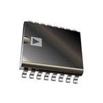
| 描述 | IC PWR DETECTOR 3.8GHZ 16-TSSOP |
| 产品分类 | |
| 品牌 | Analog Devices Inc |
| 数据手册 | |
| 产品图片 |
|
| 产品型号 | AD8362ARUZ-REEL7 |
| RF类型 | 手机,GSM,CDMA,TDMA,TETRA |
| rohs | 无铅 / 符合限制有害物质指令(RoHS)规范要求 |
| 产品系列 | - |
| 其它名称 | AD8362ARUZ-REEL7CT |
| 包装 | 剪切带 (CT) |
| 封装/外壳 | 16-TSSOP(0.173",4.40mm 宽) |
| 标准包装 | 1 |
| 电压-电源 | 4.5 V ~ 5.5 V |
| 电流-电源 | 20mA |
| 精度 | 0.5dB |
| 视频文件 | http://www.digikey.cn/classic/video.aspx?PlayerID=1364138032001&width=640&height=505&videoID=2245193150001 |
| 输入范围 | -52dBm ~ 8dBm |
| 频率 | 50Hz ~ 3.8GHz |


- 商务部:美国ITC正式对集成电路等产品启动337调查
- 曝三星4nm工艺存在良率问题 高通将骁龙8 Gen1或转产台积电
- 太阳诱电将投资9.5亿元在常州建新厂生产MLCC 预计2023年完工
- 英特尔发布欧洲新工厂建设计划 深化IDM 2.0 战略
- 台积电先进制程称霸业界 有大客户加持明年业绩稳了
- 达到5530亿美元!SIA预计今年全球半导体销售额将创下新高
- 英特尔拟将自动驾驶子公司Mobileye上市 估值或超500亿美元
- 三星加码芯片和SET,合并消费电子和移动部门,撤换高东真等 CEO
- 三星电子宣布重大人事变动 还合并消费电子和移动部门
- 海关总署:前11个月进口集成电路产品价值2.52万亿元 增长14.8%


PDF Datasheet 数据手册内容提取
50 Hz to 3.8 GHz 65 dB TruPwr™ Detector Data Sheet AD8362 FEATURES FUNCTIONAL BLOCK DIAGRAM Complete, fully calibrated measurement/control system DECL CHPF Accurate rms-to-dc conversion from 50 Hz to 3.8 GHz Input dynamic range of >65 dB: −52 dBm to +8 dBm in 50 Ω INHI Waveform and modulation independent, such as x2 CLPF GSM/CDMA/TDMA INLO Linear-in-decibels output, scaled 50 mV/dB VOUT Law conformance error of 0.5 dB VTGT x2 All functions temperature and supply stable ACOM Operates from 4.5 V to 5.5 V at 24 mA Power-down capability to 1.3 mW VSET APPLICATIONS AD8362 Power amplifier linearization/control loops VREF BIAS VPOS Transmitter power controls TRraadnisom friettqeur esnigcnya (lR sFt)r einnsgtrthum inednictaattiioonn (TSSI) COMM PWDN 02923-001 Figure 1. GENERAL DESCRIPTION Table 1. Next Generation Upgrades for the AD8362 Device No. Product Description The AD8362 is a true rms-responding power detector that has ADL5902 Improved temperature stability, single-ended a 65 dB measurement range. It is intended for use in a variety of input drive. high frequency communication systems and in instrumentation HMC1120 Improved sensitivity and range, includes envelope requiring an accurate response to signal power. It is easy to use, tracking and peak-hold function, single-ended requiring only a single supply of 5 V and a few capacitors. It input drive. operates from arbitrarily low frequencies to over 3.8 GHz and ADL5906 Improved temperature stability, single-ended accepts inputs from −52 dBm to +8 dBm with crest factors that input drive. Slightly lower input range. are typical of quadrature amplitude modulation (QAM) and AD8363 Improved temperature stability, single-ended orthogonal frequency division multiplexing (OFDM) modulation input drive. Lower input range. schemes. ADL5903 Lower range, significantly lower power consumption, single-ended input drive. The AD8362 has a 1.3 mW power consumption when powered ADL5501 Lower range, significantly lower power consumption, down by a logic high applied to the PWDN pin. It powers up linear in V/V output, single-ended input drive. within about 20 μs to its nominal operating current of 20 mA at 25°C. The AD8362 is supplied in a 16-lead TSSOP for operation over the temperature range of −40°C to +85°C. Rev. F Document Feedback Information furnished by Analog Devices is believed to be accurate and reliable. However, no responsibility is assumed by Analog Devices for its use, nor for any infringements of patents or other One Technology Way, P.O. Box 9106, Norwood, MA 02062-9106, U.S.A. rights of third parties that may result from its use. Specifications subject to change without notice. No license is granted by implication or otherwise under any patent or patent rights of Analog Devices. Tel: 781.329.4700 ©2003–2015 Analog Devices, Inc. All rights reserved. Trademarks and registered trademarks are the property of their respective owners. Technical Support www.analog.com
AD8362 Data Sheet TABLE OF CONTENTS Features .............................................................................................. 1 Operation in RF Measurement Mode .......................................... 20 Applications ....................................................................................... 1 Basic Connections ...................................................................... 20 Functional Block Diagram .............................................................. 1 Device Disable ............................................................................ 20 General Description ......................................................................... 1 Recommended Input Coupling ................................................ 20 Revision History ............................................................................... 3 Operation at Low Frequencies .................................................. 21 Specifications ..................................................................................... 4 Choosing a Value for CHPF ...................................................... 22 Absolute Maximum Ratings ............................................................ 7 Choosing a Value for CLPF ....................................................... 22 ESD Caution .................................................................................. 7 Adjusting VTGT to Accommodate Signals with Very High Crest Factors ............................................................................... 23 Pin Configuration and Function Descriptions ............................. 8 Altering the Slope ....................................................................... 23 Equivalent Circuits ........................................................................... 9 Typical Performance Characteristics ........................................... 10 Temperature Compensation and Reduction of Transfer Function Ripple .......................................................................... 24 Characterization Setup .................................................................. 16 Temperature Compensation at Various WiMAX Frequencies up Equipment ................................................................................... 16 to 3.8 GHz ........................................................................................ 25 Analysis ........................................................................................ 16 Operation in Controller Mode ................................................. 27 Circuit Description ......................................................................... 17 RMS Voltmeter with 90 dB Dynamic Range .......................... 28 Square Law Detection ................................................................ 17 AD8362 Evaluation Board ............................................................ 29 Voltage vs. Power Calibration ................................................... 18 Outline Dimensions ....................................................................... 32 Offset Elimination ...................................................................... 19 Ordering Guide .......................................................................... 32 Time-Domain Response of the Closed Loop ......................... 19 Rev. F | Page 2 of 33
Data Sheet AD8362 REVISION HISTORY 9/15—Rev. E to Rev. F 9/05—Rev. B to Rev. C Changes to General Description Section ....................................... 1 Changes to Specifications ................................................................ 3 Added Table 1; Renumbered Sequentially .................................... 1 Changes to Table 3 ............................................................................ 7 Change to Equation 3 ..................................................................... 17 Deleted Figure 16 to Figure 18; Renumbered Sequentially ....... 10 Changes to Ordering Guide ........................................................... 32 Changes to Figure 32 and Figure 33 ............................................. 13 Replaced Circuit Description Section .......................................... 15 12/12—Rev. D to Rev. E Changes to Operation in RF Measurement Mode Section ........ 18 Changes to Time Domain Response of the Closed Loop Section.. 18 Deleted Using the AD8362 Section .............................................. 20 Changes to Equation 13, Choosing a Value for CLPF Section Deleted Main Modes of Operation Section ................................. 22 and Equation 14 ............................................................................... 21 Changes to Operation in Controller Mode Section ................... 23 Changes to Ordering Guide ........................................................... 31 Changes to AD8362 Evaluation Board Section .......................... 25 Deleted General Applications Section .......................................... 29 6/07—Rev. C to Rev. D Changes to Features, General Description .................................... 1 3/04—Rev. A to Rev. B Changes to Table 1 ............................................................................ 3 Updated Format ................................................................. Universal Changes to Table 2 ............................................................................ 6 Changes to Specifications ................................................................ 3 Added Figure 21 to Figure 25 ........................................................ 11 Changes to the Offset Elimination Section ................................. 16 Changes to Equipment Section ..................................................... 15 Changes to the Operation at Low Frequencies Section ............. 17 Changes to Circuit Description Section ....................................... 16 Changes to the Time-Domain Response of the Closed Loop Changes to Single-Ended Input Drive Section ............................ 19 Section .............................................................................................. 17 Changes to Choosing a Value for CHPF section ........................ 21 Changes to Equation 13 ................................................................. 24 Changes to Choosing a Value for CLPF section ......................... 21 Changes to Table 5 .......................................................................... 31 Changes to Figure 57 ...................................................................... 23 Changes to Figure 58 ...................................................................... 24 6/03—Rev. 0 to Rev. A Added Temperature Compensation at Various WiMAX Updated Ordering Guide ................................................................. 5 Frequencies up to 3.8 GHz Section ............................................... 24 Change to Analysis Section ........................................................... 12 Changes to Ordering Guide ........................................................... 31 Updated AD8362 Evaluation Board Section ............................... 26 2/03—Revision 0: Initial Version Rev. F | Page 3 of 33
AD8362 Data Sheet SPECIFICATIONS V = 5 V, T = 25°C, Z = 50 Ω, differential input drive via balun1, VTGT connected to VREF, VOUT tied to VSET, unless otherwise noted. S O Table 2. Parameter Test Conditions/Comments Min Typ Max Unit OVERALL FUNCTION Maximum Input Frequency 3.8 GHz Input Power Range (Differential) dB referred to 50 Ω impedance level, f ≤ 2.7 GHz, into 1:4 balun1 Nominal Low End of Range −52 dBm Nominal High End of Range 8 dBm Input Voltage Range (Differential) RMS voltage at input terminals, f ≤ 2.7 GHz, into input of the device Nominal Low End of Range 1.12 mV rms Nominal High End of Range 1.12 V rms Input Power Range (S-Sided) Single-ended drive, CW input, f ≤ 2.7 GHz, into input resistive network2 Nominal Low End of Range −40 dBm Nominal High End of Range 0 dBm Input Voltage Range (S-Sided) RMS voltage at input terminals, f ≤ 2.7 GHz Nominal Low End of Range 2.23 mV rms Nominal High End of Range 2.23 V rms Input Power Range (S-Sided) Single-ended drive, CW input, f ≥ 2.7 GHz, into matched input network3 Nominal Low End of Range −35 dBm Nominal High End of Range 124 dBm Output Voltage Range R ≥ 200 Ω to ground L Nominal Low End of Range 100 mV Nominal High End of Range In general, V − 0.1 V 4.9 V S Output Scaling (Log Slope) 50 mV/dB Law Conformance Error Over central 60 dB range, f ≤ 2.7 GHz ±0.5 dB RF INPUT INTERFACE Pin INHI, Pin INLO, ac-coupled, at low frequencies Input Resistance Single-ended drive, with respect to DECL 100 Ω Differential drive 200 Ω OUTPUT INTERFACE Pin VOUT Available Output Range R ≥ 200 Ω to ground 0.1 4.9 V L Absolute Voltage Range Nominal Low End of Range Measurement mode, f = 900 MHz, P = −52 dBm 0.32 0.48 V IN Nominal High End of Range Measurement mode, f = 900 MHz, P = +8 dBm 3.44 3.52 V IN Source/Sink Current VOUT held at V/2, to 1% change 48 mA S Slew Rate Rising C = open 60 V/µs L Slew Rate Falling C = open 5 V/µs L Rise Time, 10% to 90% 0.2 V to 1.8 V, CLPF = Open 45 ns Fall Time, 90% to 10% 1.8 V to 0.2 V, CLPF = Open 0.4 µs Wideband Noise CLPF = 1000 pF, f ≤ 100 kHz 70 nV/√Hz SPOT VSET INTERFACE Pin VSET Nominal Input Voltage Range To ±1 dB error 0.5 3.75 V Input Resistance 68 kΩ Scaling (Log Slope) f = 900 MHz 46 50 54 mV/dB Scaling (Log Intercept) f = 900 MHz, into 1:4 balun −64 −60 −56 dBm −77 −73 −69 dBV VOLTAGE REFERENCE Pin VREF Output Voltage 25°C 1.225 1.25 1.275 V Temperature Sensitivity −40°C ≤ T ≤ +85°C 0.08 mV/°C A Output Resistance 8 Ω Rev. F | Page 4 of 33
Data Sheet AD8362 Parameter Test Conditions/Comments Min Typ Max Unit RMS TARGET INTERFACE Pin VTGT Nominal Input Voltage Range Measurement range = 60 dB, to ±1 dB error 0.625 2.5 V Input Bias Current VTGT = 1.25 V −28 μA VTGT = 0 V −52 μA Incremental Input Resistance 52 kΩ POWER-DOWN INTERFACE Pin PWDN Logic Level to Enable Logic low enables 1 V Logic Level to Disable Logic high disables 3 V Input Current Logic high 230 μA Logic low 5 μA Enable Time From PWDN low to VOUT within 10% of final value, CLPF = 1000 pF 14.5 ns Disable Time From PWDN high to VOUT within 10% of final value, CLPF = 1000 pF 2.5 μs POWER SUPPLY INTERFACE Pin VPOS Supply Voltage 4.5 5 5.5 V Quiescent Current 20 22 mA Supply Current When disabled 0.2 mA 900 MHz Dynamic Range Error referred to best-fit line (linear regression) ±1.0 dB linearity, CW input 65 dB ±0.5 dB linearity, CW input 62 dB Deviation vs. Temperature Deviation from output at 25°C −40°C < T < +85°C, P = −45 dBm −1.7 dB A IN −40°C < T < +85°C, P = −20 dBm −1.4 dB A IN −40°C < T < +85°C, P = +5 dBm −1.0 dB A IN Logarithmic Slope 46 50 54 mV/dB Logarithmic Intercept −64 −60 −56 dBm Deviation from CW Response 5.5 dB peak-to-rms ratio (IS95 reverse link) 0.2 dB 12.0 dB peak-to-rms ratio (W-CDMA 4 channels) 0.2 dB 18.0 dB peak-to-rms ratio (W-CDMA 15 channels) 0.5 dB 1.9 GHz Dynamic Range Error referred to best-fit line (linear regression) ±1 dB linearity, CW input 65 dB ±0.5 dB linearity, CW input 62 dB Deviation vs. Temperature Deviation from output at 25°C −40°C < T < +85°C, P = −45 dBm −0.6 dB A IN −40°C < T < +85°C, P = −20 dBm −0.5 dB A IN −40°C < T < +85°C, P = +5 dBm −0.3 dB A IN Logarithmic Slope 51 mV/dB Logarithmic Intercept −59 dBm Deviation from CW Response 5.5 dB peak-to-rms ratio (IS95 reverse link) 0.2 dB 12.0 dB peak-to-rms ratio (W-CDMA 4 channels) 0.2 dB 18.0 dB peak-to-rms ratio (W-CDMA 15 channels) 0.5 dB 2.2 GHz Dynamic Range Error referred to best-fit line (linear regression) ±1.0 dB linearity, CW input 65 dB ±0.5 dB linearity, CW input 65 dB Deviation vs. Temperature Deviation from output at 25°C −40°C < T < +85°C, P = −45 dBm −1.8 dB A IN −40°C < T < +85°C, P = −20 dBm −1.6 dB A IN −40°C < T < +85°C, P = +5 dBm −1.3 dB A IN Logarithmic Slope 50.5 mV/dB Logarithmic Intercept −61 dBm Deviation from CW Response 5.5 dB peak-to-rms ratio (IS95 reverse link) 0.2 dB 12.0 dB peak-to-rms ratio (W-CDMA 4 channels) 0.2 dB 18.0 dB peak-to-rms ratio (W-CDMA 15 channels) 0.5 dB Rev. F | Page 5 of 33
AD8362 Data Sheet Parameter Test Conditions/Comments Min Typ Max Unit 2.7 GHz Dynamic Range Error referred to best-fit line (linear regression) ±1.0 dB linearity, CW input 63 dB ±0.5 dB linearity, CW input 62 dB Deviation vs. Temperature Deviation from output at 25°C −40°C < T < +85°C, P = −40 dBm −5.3 dB A IN −40°C < T < +85°C, P = −15 dBm −5.5 dB A IN −40°C < T < +85°C, P = +5 dBm −4.8 dB A IN Logarithmic Slope 50.5 mV/dB Logarithmic Intercept −58 dBm Deviation from CW Response 5.5 dB peak-to-rms ratio (IS95 reverse link) 0.2 dB 12.0 dB peak-to-rms ratio (W-CDMA 4 channels) 0.2 dB 18.0 dB peak-to-rms ratio (W-CDMA 15 channels) 0.4 dB 3.65 GHz Single-ended drive3 Dynamic Range Error referred to best-fit line (linear regression) ±1.0 dB linearity, CW input 51 dB ±0.5 dB linearity, CW input 50 dB Deviation vs. Temperature Deviation from output at 25°C −40°C < T < +85°C, P = −35 dBm −3 dB A IN −40°C < T < +85°C, P = −15 dBm −3.5 dB A IN −40°C < T < +85°C, P = +10 dBm −3.5 dB A IN Logarithmic Slope 51.7 mV/dB Logarithmic Intercept −45 dBm 1 1:4 balun transformer, M/A-COM ETC 1.6-4-2-3. 2 See Figure 48. 3 See Figure 50. 4 The limitation of the high end of the power range is due to the test equipment not the device under test. Rev. F | Page 6 of 33
Data Sheet AD8362 ABSOLUTE MAXIMUM RATINGS Stresses at or above those listed under Absolute Maximum Table 3. Ratings may cause permanent damage to the product. This is a Parameter Rating stress rating only; functional operation of the product at these Supply Voltage VPOS 5.5 V or any other conditions above those indicated in the operational Input Power (Into Input of Device) 15 dBm section of this specification is not implied. Operation beyond Equivalent Voltage 2 V rms the maximum operating conditions for extended periods may Internal Power Dissipation 500 mW affect product reliability. θ 125°C/W JA Maximum Junction Temperature 125°C ESD CAUTION Operating Temperature Range −40°C to +85°C Storage Temperature Range −65°C to +150°C Lead Temperature (Soldering, 60 sec) 300°C Rev. F | Page 7 of 33
AD8362 Data Sheet PIN CONFIGURATION AND FUNCTION DESCRIPTIONS COMM 1 16 ACOM CHPF 2 15 VREF DECL 3 AD8362 14 VTGT INHI 4 TOP VIEW 13 VPOS (Not to Scale) INLO 5 12 VOUT DECL 6 11 VSET PWDN 7 10 ACOM COMM 8 9 CLPF 02923-002 Figure 2. Pin Configuration Table 4. Pin Function Descriptions Pin Equivalent No. Mnemonic Description Circuit 1, 8 COMM Common Connection. Connect via low impedance to system common. 2 CHPF Input HPF. Connect to common via a capacitor to determine 3 dB point of input signal high-pass filter. 3, 6 DECL Decoupling Terminals for INHI and INLO. Connect to common via a large capacitance to complete input circuit. 4, 5 INHI, INLO Differential Signal Input Terminals. Input Impedance = 200 Ω. Can also be driven single-ended, in Circuit A which case, the input impedance reduces to 100 Ω. 7 PWDN Disable/Enable Control Input. Apply logic high voltage to shut down the AD8362. 9 CLPF Connection for Ground Referenced Loop Filter Integration (Averaging) Capacitor. 10, 16 ACOM Analog Common Connection for Output Amplifier. 11 VSET Setpoint Input. Connect directly to VOUT for measurement mode. Apply setpoint input to this pin for Circuit B controller mode. 12 VOUT RMS Output. In measurement mode, VOUT is normally connected directly to VSET. Circuit C 13 VPOS Connect to 5 V Power Supply. 14 VTGT The logarithmic intercept voltage is proportional to the voltage applied to this pin. The use of a lower Circuit D target voltage increases the crest factor capacity. Normally connected to VREF. 15 VREF General-Purpose Reference Voltage Output of 1.25 V. Usually connected only to VTGT. Circuit E Rev. F | Page 8 of 33
Data Sheet AD8362 EQUIVALENT CIRCUITS DECL VPOS VPOS 50kΩ COMM VTGT VTGT 50kΩ INTERFACE ACOM GAIN = 0.12 INHI 100Ω COMM 02923-005 VGA Figure 5. Circuit C 100Ω INLO RAIL-TO-RAIL VPOS OUTPUT 0.7V VOUT VPOS 2kΩ DECL COMM 02923-003 CLPF 500Ω ACCOOMMM 02923-006 Figure 3. Circuit A Figure 6. Circuit D VPOS SOURCE ONLY VPOS REF BUF ~35kΩ VSET ~0.35V VOUT VSET ~35kΩ INTERFACE 13kΩ ACOM CAOCMOMM 02923-004 5kΩ COMM 02923-007 Figure 4. Circuit B Figure 7. Circuit E Rev. F | Page 9 of 33
AD8362 Data Sheet TYPICAL PERFORMANCE CHARACTERISTICS 4.5 4.0 3.0 4.0 100MHz 3.6 2.4 3.5 2200MHz 3.2 1.8 3.0 2.8 –40°C 1.2 B) d VOUT (V) 22..05 VOUT (V) 122...046 –00.06.6 OR IN VOUT ( 1.5 2700MHz 1.2 –+4205°°CC +85°C –1.2 ERR 1.0 0.8 +25°C –1.8 +85°C 0.5 900MHz 0.4 –2.4 1900MHz 0–60–55–50–45–40IN–3P5U–T3 A0M–2P5LI–T2U0D–E1 5(d–B1m0)–5 0 5 10 15 02923-008 –060–55 –50–45–40IN–3P5U–T3 A0M–P25LI–T2U0D–E1 5(d–B1m0)–5 0 5 10 15–3.0 02923-011 Figure 8. Output Voltage (VOUT) vs. Input Amplitude (dBm), Figure 11. VOUT and Law Conformance vs. Input Amplitude, Frequencies: 100 MHz, 900 MHz, 1900 MHz, 2200 MHz, and 2700 MHz; Frequency 1900 MHz, Sine Wave, Temperatures: −40°C, +25°C, and +85°C Sine Wave, Differential Drive 4.0 3.0 3.0 3.6 2.4 2.5 3.2 1.8 2.0 RROR IN VOUT (dB)––10011.....055050 100MH2z200MHz 1900MHz VOUT (V) 11222.....26048 –40°C +25°C –40°C +85°C ––01010..62..26 ERROR IN VOUT (dB) E 0.8 –1.8 –1.5 900MHz +85°C –2.0 0.4 +25°C –2.4 ––32..05–60–55–502–74050M–4H0zIN–3P5U–T3 A0M–2P5LI–T2U0D–E1 5(d–B1m0)–5 0 5 10 15 02923-009 0–60–55–50–45–40I–N3P5U–T3 0AM–2P5LI–T2U0D–E1 5(d–B1m0)–5 0 5 10 15–3.0 02923-012 Figure 9. Logarithmic Law Conformance vs. Input Amplitude, Figure 12. VOUT and Law Conformance vs. Input Amplitude, Frequencies: 100 MHz, 900 MHz, 1900 MHz, 2200 MHz, and 2700 MHz; Frequency 2200 MHz, Sine Wave, Temperatures: −40°C, +25°C, and +85°C Sine Wave, Differential Drive 4.0 3.0 4.0 3.6 2.4 3.5 3.2 1.8 CW 2.8 –40°C 1.2 B) 3.0 d VOUT (V) 122...604 ++852°5C°C 00–.06.6 OR IN VOUT ( VOUT (V)22..05 IS95 REVERSE LINK W-CDMA 8-CHANNEL R 1.5 W-CDMA 15-CHANNEL 1.2 –40°C –1.2 ER 1.0 0.8 –1.8 0.4 +85°C –2.4 0.5 +25°C 0–55–50–45–40I–N3P5U–T3 0AM–2P5LI–T2U0D–E1 5(d–B1m0)–5 0 5 10 15–3.0 02923-010 0–60–55–50–45–40IN–3P5U–T3 A0M–P25LI–T2U0D–E1 (5d–B1m0)–5 0 5 10 15 02923-013 Figure 10. VOUT and Law Conformance vs. Input Amplitude, Figure 13. VOUT vs. Input Amplitude with Different Waveforms, CW, IS95 Frequency 900 MHz, Sine Wave, Temperatures: −40°C, +25°C, and +85°C Reverse Link, W-CDMA 8-Channel, W-CDMA 15-Channel, Frequency 900 MHz Rev. F | Page 10 of 33
Data Sheet AD8362 3.0 4.0 2.5 3.5 2.0 1.5 3.0 dB) 1.0 W-CDMA 8-CHANNEL T ( IS95 REVERSE LINK 2.5 N VOU 0.50 CW UT (V)2.0 OR I–0.5 VO R 1.5 R–1.0 E W-CDMA 15-CHANNEL –1.5 1.0 –2.0 0.5 –2.5 –3.–060–55–50–45–40I–N3P5U–T3 A0M–2P5LI–T2U0D–E1 5(d–B1m0)–5 0 5 10 15 02923-014 0 –55–50–45–40–IN3P5U–T3 0AM–2P5L–IT2U0D–E1 5(d–B1m0)–5 0 5 10 02923-017 Figure 14. Output Error from CW Linear Reference vs. Input Amplitude Figure 17. VOUT vs. Input Amplitude, 3 Sigma to Either Side of Mean, with Different Waveforms, CW, IS95 Reverse Link, W-CDMA 8-Channel, Sine Wave, Frequency 1900 MHz, Part-to-Part Variation W-CDMA 15-Channel, Frequency 900 MHz, VTGT = 1.25 V 3.0 3.0 2.5 2.5 –40°C 2.0 2.0 1.5 1.5 dB) 1.0 4-WCH-CADNMNAEL 8-WCH-CADNMNAEL dB) 1.0 UT ( 0.5 CW UT ( 0.5 O O V V N 0 N 0 OR I–0.5 OR I–0.5 R R R–1.0 R–1.0 E W-CDMA 15-CHANNEL E –1.5 –1.5 –2.0 –2.0 +25°C +85°C –2.5 –2.5 –3.0–55–50 –45–40IN–3P5UT– 3A0M–P2L5IT–U2D0E– (1d5Bm–1)0 –5 0 5 10 02923-015 –3.0–55 –50 –45 –40 –3I5NP–U30T A–M25PL–I2T0UD–E15 (d–B1m0)–5 0 5 10 02923-018 Figure 15. Output Error from CW Linear Reference vs. Input Amplitude Figure 18. Logarithmic Law Conformance vs. Input Amplitude, with Different W-CDMA Channel Loading, 4-Channel, 8-Channel, 3 Sigma to Either Side of Mean, Sine Wave, Frequency 900 MHz, 15-Channel, Frequency 2200 MHz, VTGT = 1.25 V Temperatures: −40°C, +25°C, and +85°C 4.0 3.0 2.5 –45°C 3.5 2.0 3.0 1.5 B) d 1.0 2.5 T ( V) OU 0.5 UT (2.0 N V 0 VO OR I–0.5 1.5 R R–1.0 E 1.0 –1.5 –2.0 +25°C 0.5 +85°C –2.5 0 –55–50–45–40I–N3P5U–T3 A0M–P25LIT–2U0D–E1 (5dB–1m0) –5 0 5 10 02923-016 –3.0–55 –50 –45 –40 –3IN5P–U3T0 A–M25PL–IT2U0D–E1 5(dB–1m0) –5 0 5 10 02923-019 Figure 16. VOUT vs. Input Amplitude, 3 Sigma to Either Side of Mean, Figure 19. Logarithmic Law Conformance vs. Input Amplitude, Sine Wave, Frequency 900 MHz, Part-to-Part Variation 3 Sigma to Either Side of Mean, Sine Wave, Frequency 1900 MHz, Temperatures: −40°C, +25°C, and +85°C Rev. F | Page 11 of 33
AD8362 Data Sheet 3.0 4.0 8 +85°C 2.5 –40°C +25°C 3.5 –40°C 6 2.0 1.5 3.0 4 B) d 1.0 N VOUT ( 0.50 UT(V) 22..50 20 OR (dB) ROR I–0.5 VO 1.5 –2 ERR R–1.0 E –1.5 1.0 –4 –2.0 0.5 –6 –2.5 +85°C +25°C –3.0–55 –50 –45 –40 –3I5NP–U30T A–M25PL–I2T0UD–E15 (d–B1m0)–5 0 5 10 02923-020 0–60 –50 –40 INP–U3T0 AMP–L2I0TUDE– (1d0Bm) 0 10 20–8 02923-023 Figure 20. Logarithmic Law Conformance vs. Input Amplitude, Figure 23. VOUT and Law Conformance vs. Input Amplitude for 15 Devices, 3 Sigma to Either Side of Mean, Sine Wave, Frequency 2200 MHz, Frequency 2800 MHz, Sine Wave, Temperatures: −40°C, +25°C, and +85°C, Temperatures: −40°C, +25°C, and +85°C No Temperature Compensation, Single-Ended Drive, See Figure 50 4.0 8 4.0 8 +85°C +85°C +25°C +25°C 3.5 –40°C 6 3.5 –40°C 6 3.0 4 3.0 4 V) 2.5 2 dB) V) 2.5 2 dB) UT( 2.0 0 OR ( UT ( 2.0 0 OR ( O R O R V R V R 1.5 –2 E 1.5 –2 E 1.0 –4 1.0 –4 0.5 –6 0.5 –6 0 –8 0 –8 –60 –50 –40 INP–U3T0 AMP–L2I0TUDE– (1d0Bm) 0 10 20 02923-021 –60 –50 –40 INP–U3T0 AMP–L2I0TUDE– (1d0Bm) 0 10 20 02923-024 Figure 21. VOUT and Law Conformance vs. Input Amplitude for 15 Devices, Figure 24. VOUT and Law Conformance vs. Input Amplitude for 15 Devices, Frequency 2350 MHz, Sine Wave, Temperatures: −40°C, +25°C, and +85°C, Frequency 3450 MHz, Sine Wave, Temperatures: −40°C, +25°C, and +85°C, No Temperature Compensation, Single-Ended Drive, See Figure 50 No Temperature Compensation, Single-Ended Drive, See Figure 50 4.0 8 4.0 8 +85°C +25°C 3.5 –40°C 6 3.5 6 3.0 4 3.0 4 UT (V) 22..50 20 OR (dB) UT (V) 22..50 20 OR (dB) O R O R V R V R 1.5 –2 E 1.5 –2 E 1.0 –4 1.0 –4 0.5 –6 0.5 –6 0 –8 0 –8 –60 –50 –40 INP–U3T0 AMP–L2I0TUDE– (1d0Bm) 0 10 20 02923-022 –60 –50 –40 INP–U3T0 AMP–L2I0TUDE– (1d0Bm) 0 10 20 02923-025 Figure 22. VOUT and Law Conformance vs. Input Amplitude for 15 Devices, Figure 25. VOUT and Law Conformance vs. Input Amplitude for 15 Devices, Frequency 2600 MHz, Sine Wave, Temperatures: −40°C, +25°C, and +85°C, Frequency 3650 MHz, Sine Wave, Temperatures: −40°C, +25°C, and +85°C, No Temperature Compensation, Single-Ended Drive, See Figure 50 No Temperature Compensation, Single-Ended Drive, See Figure 50 Rev. F | Page 12 of 33
Data Sheet AD8362 52.0 2.0 1.5 51.5 +85°C B) 1.0 d 51.0 +25°C T ( 1900MHz 900MHz V) CEP 0.5 m R E (50.5 –40°C TE 0 P N SLO E IN I–0.5 50.0 G N A H–1.0 C 49.5 –1.5 2200MHz 49.0900 1000 1100 1200 1300 1400 1500FR1600EQU1700EN1800CY1900 (MH2000z)2100 2200 2300 2400 2500 2600 2700 02923-026 –2.0–40 –30 –20 –10 0 TE1M0PE2R0ATU30RE 4(°0C)50 60 70 80 90 02923-029 Figure 26. Logarithmic Slope vs. Frequency, Figure 29. Change in Logarithmic Intercept vs. Temperature, 3 Sigma to Temperatures: −40°C, +25°C, and +85°C Either Side of Mean, Frequencies: 900 MHz, 1900 MHz, and 2200 MHz –53 –54 100 –55 +85°C –56 80 m) B –57 d PT ( –58 +25°C TS60 CE HI R –59 E T 40 IN –60 –40°C –61 20 –62 –63900 1000 1100 1200 1300 1400 1500FR1600EQU1700EN1800CY1900 (MH2000z)2100 2200 2300 2400 2500 2600 2700 02923-027 048 49 S5L0OPE (mV/d5B1) 52 53 02923-030 Figure 27. Logarithmic Intercept vs. Frequency, Figure 30. Slope Distribution, Frequency 900 MHz Temperatures: −40°C, +25°C, and +85°C 3.0 80 2.5 900MHz 2.0 70 1.5 60 V) 1900MHz m 1.0 PE ( 0.5 50 N SLO 0 HITS40 E I–0.5 G 30 N–1.0 A H C–1.5 20 –2.0 2200MHz 10 –2.5 –3.0–40 –30 –20 –10 0 TE1M0PE2R0ATU30RE 4(°0C)50 60 70 80 90 02923-028 –061.0 –60.5 –60.I0NTERC–E59P.T5 (dBm–)59.0 –58.5 –58.0 02923-031 Figure 28. Change in Logarithmic Slope vs. Temperature, 3 Sigma to Either Figure 31. Logarithmic Intercept Distribution, Frequency 900 MHz Side of Mean, Frequencies: 900 MHz, 1900 MHz, and 2200 MHz Rev. F | Page 13 of 33
AD8362 Data Sheet 5.0 6 5.0 6 4.5 RF BURST 4 4.5 4 ENABLE 2V/DIV 2V/DIV 4.0 2 4.0 2 3.5 0 V) 3.5 0 V) +2dBm E ( +2dBm N ( VOUT (V) 322...005 VOUT ––2100ddBBmm –––264 URST ENABL VOUT (V)322...005 ––2100ddBBmm –––264 ER-DOWN PI 1.5 0.5V/DIV –30dBm –8 RF B 1.50.5V/DIV –30dBm –8 POW 1.0 –10 1.0 –10 0.5 –12 0.5 –12 00 2 4 6 8TIM1E0 (µs)12 14 16 18 20–14 02923-032 00 2 4 6 8TIME1 0(ms)12 14 16 18 20–14 02923-035 Figure 32. Output Response to RF Burst Input for Various Figure 35. Output Response Using Power-Down Mode for Various RF Input RF Input Levels, Carrier Frequency 900 MHz, CLPF = Open Levels, Carrier Frequency 900 MHz, CLPF = 0.1 µF 5.0 6 5.5 6 4.5 RF BURST 2V/DIV 4 5.0 VPOS 2V/DIV 4 ENABLE 4.0 2 4.5 2 3.5 0 V) 4.0 0 V) +2dBm E ( N ( VOUT (V) 3221....0055 VOUT –––213000dddBBBmmm ––––2648 RF BURST ENABL VOUT (V)3232....5500 1V/DIV ––21+002dddBBBmmm ––––2648 POWER-DOWN PI 1.0 –10 1.5 –30dBm –10 0.5V/DIV 0.5 –12 1.0 –12 00 2 4 6 8TIME1 0(ms)12 14 16 18 20–14 02923-033 00 2 4 6 8TIME10 (ms)12 14 16 18 20–14 02923-036 Figure 33. Output Response to RF Burst Input for Various RF Input Levels, Figure 36. Output Response to Gating on Power Supply for Various RF Input Carrier Frequency 900 MHz, CLPF = 0.1 µF Levels, Carrier Frequency 900 MHz, CLPF = 0 5.0 6 4.5 4 POWER- 2V/DIV 4.0 DOWN 2 PIN 3.5 0 V) VOUT +2dBm N ( UT (V)32..05 –10dBm ––24 OWN PI 100MHz VO2.0 0.5V/DIV ––2300ddBBmm –6 WER-D 3GHz 1.5 –8 PO 1.0 –10 0.5 –12 00 2 4 6 8TIME10 (µs)12 14 16 18 20–14 02923-034 02923-037 Figure 34. Output Response Using Power-Down Mode for Various RF Input Figure 37. INHI, INLO Differential Input Impedance, 100 MHz to 3 GHz Levels, Carrier Frequency 900 MHz, CLPF = 0 Rev. F | Page 14 of 33
Data Sheet AD8362 5 300 0 250 V) m –5 EF ( 200 R N V –10 TS E I HI150 G –15 N A H C 100 –20 –25 50 –30–40 –30 –20 –10 0TEM10PER2A0TU3R0E (°4C0) 50 60 70 80 90 02923-038 1.0230 1.235 1.240 1.245 V1R.2E5F0 (V)1.255 1.260 1.265 1.270 02923-039 Figure 38. Change in VREF vs. Temperature, 3 Sigma to Either Side of Mean Figure 39. VREF Distribution Rev. F | Page 15 of 33
AD8362 Data Sheet CHARACTERIZATION SETUP EQUIPMENT TEK TDS5104 AD8362 The general hardware configuration used for most of the AD8362 SCOPE TEK P5050 COMM ACOM characterization is shown in Figure 40. The signal source is a VOLTAGE PROBE CHPF VREF Rohde & Schwarz SMIQ03B. A 1:4 balun transformer is used to C1 transform the single-ended RF signal to differential form. For DECL VTGT HPE3631A frequencies above 3.0 GHz, an Agilent 8521A signal source was INHI VPOS POWER used. For the response measurements in Figure 32 and Figure 33, SSIMGNT0A3L 3dB BALUN SUPPLY GENERATOR INLO VOUT the configuration shown in Figure 41 is used. For Figure 34 and C2 DECL VSET Figure 35, the configuration shown in Figure 42 is used. For RF 50Ω C3 PWDN ACOM Figure 36, the configuration shown in Figure 43 is used. COMM CLPF CHARAABCDOT8AE3RR6IDZ2ATION C4 02923-041 SMIQ03B MULTIMETER Figure 41. Response Measurement Setup for Modulated Pulse RF SOURCE 3dB RFIN VOUT HP34401A TEK TDS5104 AD8362 SCOPE TEK P5050 COMM ACOM VOLTAGE PROBE CONTPRCOLLER 02923-040 C1 CHPF VREF Figure 40. Primary Characterization Setup DECL VTGT HPE3631A ANALYSIS SSIMGNT0A3L 3dB BALUN INHI VPOS SPUOPWPELRY GENERATOR INLO VOUT The slope and intercept are derived using the coefficients of C2 a linear regression performed on data collected in its central RF 50Ω C3 DECL VSET operating range. Error is stated in two forms: error from the HP8112A PWDN ACOM PULSE linear response to the CW waveform and output delta from GENERATOR COMM CLPF 25°C performance. C4 02923-042 The error from linear response to the CW waveform is the Figure 42. Response Measurement Setup for Power-Down Step decibel difference in output from the ideal output defined by the conversion gain and output reference. This is a measure of HP8112A the linearity of the device response to both CW and modulated AD811 PULSE GENERATOR waveforms. The error in dB is calculated by 50Ω 732Ω VOUTSlope P P ErrordB IN Z (1) Slope where P is the x intercept, expressed in dBm. AD8362 TEK TDS5104 Z SCOPE COMM ACOM Error from the linear response to the CW waveform is not a CHPF VREF measure of absolute accuracy because it is calculated using C1 TEK P5050 VOLTAGE the slope and intercept of each device. However, it verifies the DECL VTGT PROBE linearity and the effect of modulation on the device response. INHI VPOS Error from the 25°C performance uses the performance of a 3dB BALUN 0.01µF 100pF INLO VOUT given device and waveform type as the reference; it is predomi- C2 DECL VSET nantly a measurement of output variation with temperature. C3 SMT03 PWDN ACOM SIGNAL GENREFR 5A0TΩOR COMM CLPF C4 02923-043 Figure 43. Response Measurement Setup for Gated Supply Rev. F | Page 16 of 33
Data Sheet AD8362 CIRCUIT DESCRIPTION The AD8362 is a fully calibrated, high accuracy, rms-to-dc The VGA gain has the form converter providing a measurement range of over 65 dB. It is G = G exp(−V /V ) (2) SET O SET GNS capable of operating from signals as low in frequency as a few where: hertz to at least 3.8 GHz. Unlike earlier rms-to-dc converters, G is a basic fixed gain. the response bandwidth is completely independent of the signal O V is a scaling voltage that defines the gain slope (the dB magnitude. The −3 dB point occurs at about 3.5 GHz. The GNS change per volt). Note that the gain decreases with V . capacity of this device to accurately measure waveforms having a SET high peak-to-rms ratio (crest factor) is independent of either The VGA output is the signal frequency or its absolute magnitude, over a wide V = G V = G V exp(−V /V ) (3) SIG SET IN O IN SET GNS range of conditions. where V is the ac voltage applied to the input terminals IN This unique combination allows the AD8362 to be used as a of the AD8362. calibrated RF wattmeter covering a power ratio of >1,000,000:1, As explained in the Recommended Input Coupling section, the a power controller in closed-loop systems, a general-purpose input drive can either be single-sided or differential, although rms-responding voltmeter, and in many other low frequency dynamic range is maximized with a differential input drive. The applications. effect of high frequency imbalances when using a single-sided The device comprises the core elements of a high performance drive is less apparent at low frequencies (from 50 Hz to 500 MHz), AGC loop (see Figure 44), laser-trimmed during manufacturing but the peak input voltage capacity is always halved relative to to close tolerances while fully operational at a test frequency of differential operation. 100 MHz. Its linear, wideband VGA provides a general voltage SQUARE LAW DETECTION gain, G ; this can be controlled in a precisely exponential (linear- SET in-dB) manner over the full 68 dB range from −25 dB to +43 dB The output of the variable gain amplifier (V ) is applied to SIG by a voltage, V . However, to provide adequate guardbanding, a wideband square law detector, which provides a true rms SET only the central 60 dB of this range, from −21 dB to +39 dB, is response to this alternating signal that is essentially independent normally used. The Adjusting VTGT to Accommodate Signals of waveform. Its output is a fluctuating current (I ) that has SQU with Very High Crest Factors section shows how this basic a positive mean value. This current is integrated by an on-chip range can be shifted up or down. capacitance (C), which is usually augmented by an external F AMPLITUDETARGET capacitance (CLPF) to extend the averaging time. The resulting –25dBTO+43dB MATCH WIDE- FOR VSIG voltage is buffered by a gain of 5, dc-coupled amplifier whose BAND SQUARERS INHI VTGT rail-to-rail output (VOUT) can be used for either measurement VGA X2 X2 × 0.06 or control purposes. INLO VSIG VATG ACOM In most applications, the AGC loop is closed via the setpoint ISQU ITGT interface pin, VSET, to which the VGA gain control voltage on CHPF GSET OFFSET VOUT is applied. In measurement modes, the closure is direct NULLING CF OUTPUT and local by a simple connection from the output of the VOUT FILTER VOUT pin to the VSET pin. In controller modes, the feedback path is around some larger system, but the operation is the same. VSET SETPOINT INTERFACE CLPF The fluctuating current (ISQU) is balanced against a fixed setpoint target current (I ) using current mode subtraction. INTERNAL TGT RESISTORS With the exact integration provided by the capacitor(s), the SET BUFFER BAND GAP GAIN TO 5 AGC loop equilibrates when VREF REFERENCE 1.25V MEAN(I ) = I (4) EXTERCNLAPLF ACOM 02923-044 The current, ISTQGUT, is pTrGoTvided by a second-reference squaring Figure 44. Basic Structure of the AD8362 cell whose input is the amplitude-target voltage VATG. This is a fraction of the voltage VTGT applied to a special interface, which accepts this input at the VTGT pin. Because the two squaring cells are electrically identical and are carefully imple- mented in the IC, process and temperature-dependent variations in the detailed behavior of the two square-law functions cancel. Rev. F | Page 17 of 33
AD8362 Data Sheet Accordingly, VTGT (and its fractional part V ) determines In practice, the response deviates slightly from the ideal straight ATG the output that must be provided by the VGA for the AGC loop line suggested by Equation 11. This deviation is called the law to settle. Because the scaling parameters of the two squarers are conformance error. In defining the performance of high accuracy accurately matched, it follows that Equation 4 is satisfied only when measurement devices, it is customary to provide plots of this error. In general terms, it is computed by extracting the best MEAN(V 2) = V 2 (5) SIG ATG straight line to the measured data using linear regression over In a formal solution, extract the square root of both sides to provide a substantial region of the dynamic range and under clearly an explicit value for the root-mean-square (rms) value. However, it specified conditions. is apparent that by forcing this identity through varying the VGA 3.0 gain and extracting the mean value by the filter provided by the 3.8 2.5 capacitor(s), the system inherently establishes the relationship 3.5 2.0 3.2 –40°C rms(VSIG) = VATG (6) 1.5 2.9 Substituting the value of VSIG from Equation 3, V) 22..36 01..50 UT (dB) rms[GOVIN exp(−VSET/VGNS)] = VATG (7) OUT ( 2.0 0 N VO Aotsh ae rm peaarsaumreemteresn ct adne vbiec ef,i xVeIdN bisy t dhees uignnk. nToow sno lqvue aEnqtuitayt aionnd 7a,l l V 11..47 +25°C +85°C ––10..05 RROR I E 1.1 –40°C –1.5 rms[GOVIN/VATG] = exp(VSET/VGNS) (8) 0.8 +25°C –2.0 therefore, 0.5 +85°C –2.5 0.2 The qVuSaEnTti t=y VVGZN =S lVogAT[Grm/GsO( VisI Nd)e/fVinZ]e d as the intercept voltage (9) –60–55–50–45–40IN–3P5UT–3 A0M–P25LI–T2U0D–E1 (5d–B1m0)–5 0 5 10 15–3.0 02923-045 Figure 45. Output Voltage and Law Conformance Error because VSET must be 0 when rms (V ) = V . IN Z at TA = −40°C, +25°C, and +85°C When connected as a measurement device, the output of the Figure 45 shows the output of the circuit of Figure 47 over the buffer is tied directly to VSET, which closes the AGC loop. full input range. The agreement with the ideal function (law Making the substitution VOUT = VSET and changing the conformance) is also shown. This was determined by linear log base to 10, as needed in a decibel conversion, regression on the data points over the central portion of the VOUT = VSLP log10[rms(VIN)/VZ] (10) transfer function for the +25°C data. where VSLP is the slope voltage, that is, the change in output The error at −40°C, +25°C, and +85°C was then calculated by voltage for each decade of change in the input amplitude. subtracting the ideal output voltage at each input signal level Note that VSLP = VGNS log (10) = 2.303 VGNS. from the actual output and dividing this quantity by the mean In the AD8362, V is laser-trimmed to 1 V using a 100 MHz slope of the regression equation to provide a measurement of SLP test signal. Because a decade corresponds to 20 dB, this slope the error in decibels (scaled on the right-hand axis of Figure 45). can also be stated as 50 mV/dB. The Altering the Slope section The error curves generated in this way reveal not only the devia- explains how the effective value of VSLP can be altered by the tions from the ideal transfer function at a nominal temperature, user. The intercept, VZ, is also laser-trimmed to 224 µV (−60 dBm but also the additional errors caused by temperature changes. relative to 50 Ω). In an ideal system, VOUT would cross zero Notice that there is a small temperature dependence in the for an rms input of that value. In a single-supply realization of intercept (the vertical position of the error plots). the function, VOUT cannot run fully down to ground; here, V Z Figure 45 further reveals a periodic ripple in the conformance is the extrapolated value. curves. This is due to the interpolation technique used to select VOLTAGE vs. POWER CALIBRATION the signals from the attenuator, not only at discrete tap points, The AD8362 can be used as an accurate rms voltmeter from but also anywhere in between, thus providing continuous arbitrarily low frequencies to microwave frequencies. For low attenuation values. The selected signal is then applied to the frequency operation, the input is usually specified either in 3.5 GHz, 40 dB fixed gain amplifier in the remaining stages of volts rms or in dBV (decibels relative to 1 V rms). the VGA of the AD8362. At high frequencies, signal levels are commonly specified in power terms. In these circumstances, the source and termina- tion impedances are an essential part of the overall scaling. For this condition, the output voltage can be expressed as VOUT = SLOPE × (P − P ) (11) IN Z where P and the intercept P are expressed in dBm. IN Z Rev. F | Page 18 of 33
Data Sheet AD8362 An approximate schematic of the signal input section of the When using the AD8362 in low frequency applications, the AD8362 is shown in Figure 46. The ladder attenuator is com- corner frequency can be reduced as needed by the addition of a posed of 11 sections (12 taps), each of which progressively capacitor from the CHPF pin to ground having a nominal value attenuates the input signal by 6.33 dB. Each tap is connected to of 200 μF/Hz. a variable transconductance cell whose bias current determines For example, to lower the high-pass corner frequency to the signal weighting given to that tap. The interpolator determines 150 Hz, a capacitance of 1.33 μF is required. The offset voltage which stages are active by generating a discrete set of bias currents, varies depending on the actual gain at which the VGA is each having a Gaussian profile. These are arranged to move operating, and thus on the input signal amplitude. from left to right, thereby determining the attenuation applied Baseline variations of this sort are a common aspect of all to the input signal as the gain is progressively lowered over the VGAs, but they are more evident in the AD8362 because of the 69.3 dB range under control of the VSET input. The detailed method of its implementation, which causes the offsets to ripple manner in which the transconductance of adjacent stages varies along the gain axis with a period of 6.33 dB. When an excessively as the virtual tap point slides along the attenuator accounts for large value of CHPF is used, the offset correction process can the ripple observed in the conformance curves. Its magnitude is lag the more rapid changes in the gain of the VGA, which in slightly temperature dependent and varies with frequency (see turn can increase the time required for the loop to fully settle Figure 10, Figure 11, and Figure 12). Notice that the system for a given steady input amplitude. responses to signal inputs at INHI and INLO are not completely independent; these pins do not constitute a fully floating TIME-DOMAIN RESPONSE OF THE CLOSED LOOP differential input. The external low-pass averaging capacitance (CLPF) added at the output of the squaring cell is chosen to provide adequate GAUSSIAN INTERPOLATOR ACTOTNETNRUOALTION filtering of the fluctuating detected signal. The optimum value depends on the application; as a guideline, a value of roughly TO FIXED GAIN STAGE 900 μF/Hz should be used. For example, a capacitance of 5 μF gm gm gm gm provides adequate filtering down to 180 Hz. Note that the INHI fluctuation in the quasi-dc output of a squaring cell operating on a sine wave input is a raised cosine at twice the signal frequency, easing this filtering function. DECL In the standard connections for the measurement mode, the VSET pin is tied to VOUT. For small changes in input ampli- tude (a few decibels), the time-domain response of this loop INLO S6.T3A3dGBE 1 S6.T3A3dGBE 2 S6.T3A3dGBE 11 02923-046 inso emssiennatlilayl lfy l =in 1ea/(r2, πw i×th C aL 3P Fd B× l1o1w0-0p)a. sIsn cteorrnnaelr t fimreqe udeenlacyys of Figure 46. Simplified Input Circuit LP around this local loop set the minimum recommended value OFFSET ELIMINATION of this capacitor to about 300 pF, resulting in an f of LP To address the small dc offsets that arise in the VGA, an offset- approximately 500 kHz. nulling loop is used. The high-pass corner frequency of this When large and abrupt changes of input amplitude occur, loop is internally preset to 1 MHz, which is sufficiently low for the loop response becomes nonlinear and exhibits slew rate most high frequency applications. limitations. Rev. F | Page 19 of 33
AD8362 Data Sheet OPERATION IN RF MEASUREMENT MODE BASIC CONNECTIONS The balun outputs must be ac-coupled to the input of the AD8362. The balun used in this example (M/A-COM ETC Basic connections for operating the AD8362 in measurement 1.6-4-2-3) is specified for operation from 0.5 GHz to 2.5 GHz. mode are shown in Figure 47. While the AD8362 requires a single supply of nominally 5 V, its performance is essentially If a center-tapped, flux-coupled transformer is used, connect unaffected by variations of up to ±10%. the center tap to the DECL pins, which are biased to the same potential as the inputs (approximately 3.6 V). The supply is connected to the VPOS pin using the decoupling network also displayed in Figure 47. The capacitors used in this At lower frequencies where impedance matching is not neces- network must provide a low impedance over the full frequency sary, the AD8362 can be driven from a low impedance differential range of the input and should be placed as close as possible to source, remembering the inputs must be ac-coupled. the VPOS pin. Two different capacitors are used in parallel to Choosing Input Coupling Capacitors reduce the overall impedance because these have different reso- As noted, the inputs must be ac-coupled. The input coupling nant frequencies. The measurement accuracy is not critically capacitors combine with the 200 Ω input impedance to create dependent on supply decoupling because the high frequency an input high pass corner frequency equal to signal path is confined to the relevant input pins. Lead lengths from both DECL pins to ground and from INHI/INLO to the fHP = 1/(200 × π × CC) (12) input coupling capacitors should be as short as possible. All Typically, f should be set to at least one tenth the lowest input HP COMM pins should also connect directly to the ground plane. frequency of interest. To place the device in measurement mode, connect VOUT to Single-Ended Input Drive VSET and connect VTGT directly to VREF. As previously noted, the input stages of the AD8362 are optimally DEVICE DISABLE driven from a fully balanced source, which should be provided The AD8362 is disabled by a logic high on the PWDN pin, wherever possible. In many cases, unbalanced sources can be which can be directly grounded for continuous operation. applied directly to one or the other of the two input pins. The When enabled, the supply current is nominally 20 mA and chief disadvantage of this driving method is a 10 dB to 15 dB essentially independent of supply voltage and input signal reduction in dynamic range at frequencies above 500 MHz. strength. When powered down by a logic low on PWDN, Figure 48 illustrates one of many ways of coupling the signal the supply current is reduced to 230 μA. source to the AD8362. Because the input pins are biased to RECOMMENDED INPUT COUPLING about 3.6 V (for VS = 5 V), dc-blocking capacitors are required when driving from a grounded source. For signal frequencies The full dynamic range of the AD8362, particularly at very >5 MHz, a value of 1 nF is adequate. While either INHI or high frequencies (above 500 MHz), is realized only when the INLO can be used, INHI is chosen here. input is presented to it in differential (balanced) form. In Figure 47, AD8362 a transmission line balun is used at the input. Having a 1:4 impedance ratio (1:2 turns ratio), the 200 Ω differential input 1 COMM ACOM 16 0.01µF resistance of the AD8362 becomes 50 Ω at the input to the balun. 2 CHPF VREF 15 1nF 3 DECL VTGT 14 1nF VS RF INPUT 4 INHI VPOS 13 5V @ 24mA 100Ω 1nF AD8362 5 INLO VOUT 12 1:4 Z-RATIO C8 1 COMM ACOM 16 C1 1nF 6 DECL VSET 11 C10 1000pF 2 CHPF VREF 15 0.1µF 7 PWDN ACOM 10 SZI IG=NNP50UAΩTL 1000pF 10C06pF 1CnF4 34 DINEHCIL VVPTOGST 1143 1Cn2F 8 COMM CLPF 9 02923-048 C7 5 INLO VOUT 12 VOUT Figure 48. Input Coupling from a Single-Ended 50 Ω Source T1 10C05pF 1nF 6 DECL VSET 11 ETC1.6-4-2-3 7 PWDN ACOM 10 8 COMM CLPF 90.C13µF 02923-047 Figure 47. Basic Connections for RF Power Measurement Rev. F | Page 20 of 33
Data Sheet AD8362 An external 100 Ω shunt resistor combines with the internal 3.00 3.0 100 Ω single-ended input impedance to provide a broadband 2.75 23..84G5GHHzz 2.5 50 Ω match. The unused input (in this case, INLO) is ac-coupled 2.50 3.65GHz 2.0 to ground. Figure 49 shows the transfer function of the AD8362 2.25 1.5 at various frequencies when the RF input is driven single- 2.00 1.0 etonpd eedn.d T ohfe t hrees rualntsg seh ios wd etghraatd terdan bsyfe trh feu snicntgiolen- elnindeeadr idtyr iavte t. he OUT (V)11..7550 00.5 ROR (dB) V1.25 –0.5 R 4.0 2.0 E 450MHz 1.00 –1.0 1900MHz 3.5 2500MHz 1.5 0.75 –1.5 900MHz 2140MHz 0.50 –2.0 3.0 1.0 0.25 –2.5 OUT (V) 22..50 00.5 ROR (dB) 0–60 –55 –50 –45 –40IN–3P5UT–3 A0M–P25LIT–2U0DE–1 5(dB–1m0)–5 0 5 10 15–3.0 02923-051 V R Figure 51. Transfer Function at Various Frequencies ≥2.7 GHz when 1.5 –0.5 E the RF Input is Driven Single-Ended 1.0 –1.0 OPERATION AT LOW FREQUENCIES 0.5 –1.5 In conventional rms-to-dc converters based on junction tech- niques, the effective signal bandwidth is proportional to the 0–55 –50 –45 –40 –35 –30P–IN25 (d–B2m0)–15 –10 –5 0 5 10–2.0 02923-049 sthigen AalD a8m3p6l2it iusd ien.d Ienp ceonndternats to, ft hites 3g.a5i nG. HBezc VauGsAe tbhaisn damwipdltifhi eirn is Figure 49. Transfer Function at Various Frequencies when the internally dc-coupled, the system is also used as a high accuracy RF Input is Driven Single-Ended rms voltmeter at low frequencies, retaining its temperature- AD8362 stable, decibel-scaled output (for example, in seismic, audio, 1 COMM ACOM 16 0.01µF and sonar instrumentation). 2 CHPF VREF 15 RF INPUT 2.7nH 1nF 3 DECL VTGT 14 While the AD8362 can be operated at arbitrarily low frequencies, 4 INHI VPOS 13 an ac-coupled input interface must be maintained. In such cases, 4.7nH 1nF 1nF 5 INLO VOUT 12 the input coupling capacitors should be large enough so that the 1nF 6 DECL VSET 11 lowest frequency components of the signal to be included in the 7 PWDN ACOM 10 measurement are minimally attenuated. For example, for a 3 dB 8 COMM CLPF 9 02923-050 rinedpuutc trieosnis atat n1c.5e kisH 1z0,0 c Ωap aatc ietaacnhc eisn pouf t1 pµiFn a(2re0 0n eΩed deidff ebreecnatuiaslel yt)h,e Figure 50. Input Matching for Operation at Frequencies ≥2.7 GHz and the calculation is 1/(2π × 1.5 kΩ × 100) = 1 μF. In addition, to lower the high-pass corner frequency of the VGA, a large capaci- For operation at frequencies ≥2.7 GHz, some additional tor must be connected between the CHPF pin and ground (see components are required to match the AD8362 input to 50 Ω the Choosing a Value for CHPF section). (see Figure 50). As the operating frequency increases, there is also corresponding shifting in the operating power range (see More information on the operation of the AD8362 and other Figure 51). RF power detectors at low frequency is available in AN-691 Application Note, Operation of RF Detector Products at Low Frequency. Rev. F | Page 21 of 33
AD8362 Data Sheet CHOOSING A VALUE FOR CHPF This is due to the presence of significant low frequency components in the complex, pseudorandom modulation, which The 3.5 GHz VGA of the AD8362 includes an offset cancel- generates fluctuations in the output of the AD8362. Increasing lation loop, which introduces a high-pass filter effect in its CLPF also increases the step response of the AD8362 to a transfer function. To measure the amplitude of the input signal change at its input. properly, the corner frequency (f ) of this filter must be well HP below that of the lowest input signal in the desired measurement Table 5 shows recommended values of CLPF for popular bandwidth frequency. The required value of the external modulation schemes. In each case, CLPF is increased until capacitor is given by residual output noise falls below 50 mV. A 10% to 90% step response to an input step is also listed. Where the increased CHPF = 1/(2π × 800 × f ) (13) HP response time is unacceptably high, CLPF must be reduced. If For operation at frequencies as low as 100 kHz, set f to HP the output of the AD8362 is sampled by an ADC, averaging in approximately 25 kHz (CHPF = 8 nF). For frequencies above the digital domain can further reduce the residual noise. approximately 2 MHz, no external capacitance is required Figure 52 shows how residual ripple and rise/fall time vary with because there is adequate internal capacitance on this node. filter capacitance when the AD8362 is driven by a single carrier CHOOSING A VALUE FOR CLPF W-CDMA signal (Test Model 1-64) at 2140 MHz. In the standard connections for the measurement mode, the 180 18 170 17 VSET pin is tied to VOUT. For small changes in input ampli- 160 16 tude such as a few decibels, the time-domain response of this 150 15 olaorfoo npuo nimsd ie tnshsaielsln ylto ifacLPla l=ly l ol1ion/(pe2a πsre ×wt tiChtheL Pam F3i n ×di Bm1 1luo0mw0) -r.p eIacnsotsem rcnmoarenl nteidrm efdree dvqeaulleaunyesc y E (mV p-p)111143210000 RESIDUAL RIPPLE (mV p-p) 11114321 ME (ms) PL100 10 TI Fofo rth oips ecraaptaiocnit oart tloow abero usitg 3n0a0l fprFe,q mueankciinegs ,f oLPr =w 5h0e0n ekvHerz .t he UAL RIP 987000 FALL TIME (ms) 987 E/FALL averaging time needs to be longer, use ESID 6500 65 RIS R 40 4 CLPF = 1/(2π × fLP × 1100) (14) 30 RISE TIME (ms) 3 20 2 When the input signal exhibits large crest factors, such as a 10 1 CmDigMhtA s eoerm W n-eCcDesMsaAry .s ignal, CLPF must be much larger than 00 0.1 0.2 0F.I3LTER0. 4CAP0A.C5ITA0N.C6E (µ0F.7) 0.8 0.9 1.00 02923-052 Figure 52. Residual Ripple, Rise and Fall Time vs. Filter Capacitance, Single Carrier W-CDMA Input Signal, Test Model 1-64 Table 5. Recommended CLPF Values for Various Modulation Schemes Response Time (Rise/Fall) Modulation Scheme/Standard Crest Factor CLPF Residual Ripple 10% to 90% W-CDMA , Single-Carrier, Test Model 1-64 12.0 dB 0.1 µF 28 mV p-p 171 µs/1.57 ms W-CDMA, 4-Carrier, Test Model 1-64 11.0 dB 0.1 µF 20 mV p-p 162 µs/1.55 ms CDMA2000, Single-Carrier, 9CH Test Model 9.1 dB 0.1 µF 38 mV p-p 179 µs /1.55 ms CDMA2000, 3-Carrier, 9CH Test Model 11.0 dB 0.1 µF 29 mV p-p 171 µs/1.55 ms WiMAX 802.16 (64QAM, 256 Subcarriers, 10 MHz Bandwidth) 14.0 dB 0.1 µF 30 mV p-p 157 µs/1.47 ms Rev. F | Page 22 of 33
Data Sheet AD8362 ADJUSTING VTGT TO ACCOMMODATE SIGNALS 4.0 2.0 VOUT CW WITH VERY HIGH CREST FACTORS VOUT 64QAM 3.5 VOUT WCDMA TM1-64 1.5 VOUT QPSK An external direct connection between VREF (1.25 V) and VTGT 3.0 VOUT 256QAM 1.0 sets up the internal target voltage, which is the rms voltage that must be provided by the VGA to balance the AGC feedback loop. V) 2.5 0.5 dB) In the default scheme, the VREF of 1.25 V positions this target UT ( 2.0 0 OR ( O R to 0.06 × 1.25 V = 75 mV. In principle, however, VTGT can be V R 1.5 –0.5 E driven by voltages that are larger or smaller than 75 mV. This technique can be used to move the intercept, which increases or 1.0 –1.0 ERROR QPSK 4dB CF decreases the input sensitivity of the device, or to improve the ERROR 256QAM 8.2dB CF 0.5 ERROR CW –1.5 accuracy when measuring signals with large crest factors. ERROR 64QAM 7.7dB CF ERROR WCDMA TM1-64 10.6dB CF Freosri setxivaem apttleen, iuf atthoirs opfi n1 iksΩ su:1p pkΩlie,d t hfreo omu tVpuRtE rFe qvuiair ae ds ifmropmle the 0–65–60–55–50–45–40–35P–IN30 (d–B2m5)–20–15–10 –5 0 5 10–2.0 02923-054 VGA is halved to 37.5 mV rms. Under these conditions, the Figure 54. Transfer Function and Law Conformance for Signals with Varying Crest Factors, VTGT = 0.625 V, CLPF = 0.1 μF effective headroom in the signal path that drives the squaring cell is doubled. In principle, this doubles the peak crest factor Reducing VTGT also reduces the intercept. More significant in that can be handled by the system. this case, however, is the behavior of the error curves. Note that in Figure 54 all of the error curves sit on one another, while in Figure 53 and Figure 54 show the effect of varying VTGT on Figure 53, there is some vertical spreading. This suggests that measurement accuracy when the AD8362 is swept with a series VTGT should be reduced in those applications where a wide of signals with different crest factors, varying from CW with a range of input crest factors is expected. As noted, VTGT can crest factor of 3 dB, to a W-CDMA carrier (Test Model 1-64) also be increased above its nominal level of 1.25 V. While this with a crest factor of 10.6 dB. The crest factors of each signal are can be used to increase the intercept, it would have the undesir- listed in the plots. In Figure 53, VTGT is set to its nominal value able effect of degrading measurement accuracy in situations of 1.25 V, while in Figure 54, it is reduced to 0.625 V. where the crest factor of the signal being measured varies 4.0 2.0 significantly. VOUT CW VOUT 64QAM 3.5 VOUT WCDMA TM1-64 1.5 ALTERING THE SLOPE VOUT QPSK 3.0 VOUT256QAM 1.0 None of the changes in operating conditions discussed so far affects the logarithmic slope (V ) in Equation 10. This can 2.5 0.5 SLP V) dB) readily be altered by controlling the fraction of VOUT that is UT ( 2.0 0 OR ( fed back to the setpoint interface at the VSET pin. When the full O R V R signal from VOUT is applied to VSET, the slope assumes its 1.5 –0.5 E nominal value of 50 mV/dB. It can be increased by including a 1.0 ERROR QPSK 4dB CF –1.0 voltage divider between these pins, as shown in Figure 55. ERROR 256QAM 8.2dB CF 0.5 EERRRROORR 6C4WQAM 7.7dB CF –1.5 AD8362 ERROR WCDMA TM1-64 10.6dB CF 1 COMM ACOM 16 0–65–60–55–50–45–40–35P–IN30 (d–B2m5)–20–15–10 –5 0 5 10–2.0 02923-053 23 CDHECPFL VVRTGEFT 1154 Figure 53. Transfer Function and Law Conformance for Signals with 4 INHI VPOS 13 Varying Crest Factors, VTGT = 1.25 V 5 INLO VOUT 12 VOUT R1 6 DECL VSET 11 7 PWDN ACOM 10 R2 8 COMM CLPF 9 02923-055 Figure 55. External Network to Raise Slope Rev. F | Page 23 of 33
AD8362 Data Sheet Moderately low resistance values should be used to minimize 4.0 2 scaling errors due to the 70 kΩ input resistance at the VSET pin. 3.5 This resistor string also loads the output, and it eventually reduces the load-driving capabilities if very low values are used. To 3.0 1 calculate the resistor values, use R1 = R2' (SD/50 − 1) (15) UT (V)22..50 ERROR (dB –40°C) 0 OR (dB) where: VO RR 1.5 E S is the desired slope, expressed in mV/dB. D ERROR (dB +25°C) R2' is the value of R2 in parallel with 70 kΩ. 1.0 –1 ERROR (dB +85°C) For example, using R1 = 1.65 kΩ and R2 = 1.69 kΩ (R2' = 0.5 VVOOUUTT((+–4205°°CC)) 1.649 kΩ), the nominal slope is increased to 100 mV/dB. VOUT(+85°C) tNhoet me, ahxoiwmeuvmer ,i nthpautt d soigunbaliln tgo tahpep srlooxpime iant etlhyi s− m10a dnBnmer rbeedcuaucesse 0–60 –50 –40 –30PIN (d–B20m) –10 0 10 –2 02923-056 of the limited swing of VOUT (4.9 V with a 5 V power supply). Figure 56. Transfer Function and Linearity with Combined Ripple Reduction and Temperature Compensation Circuits, Frequency = 2.14 GHz, TEMPERATURE COMPENSATION AND REDUCTION Single-Carrier W-CDMA, Test Model 1-64 OF TRANSFER FUNCTION RIPPLE Because of the reduced filter capacitor, the rms voltage appearing The transfer function ripple and intercept drift of the AD8362 at the output of the error amplifier now contains significant can be reduced using two techniques detailed in Figure 57. peak-to-peak noise. While it is critical to feed this signal back to CLPF is reduced from its nominal value. For broadband- the VGA gain control input with the noise intact, the rms voltage modulated input signals, this results in increased noise at the going to the external measurement node can be filtered using a output that is fed back to the VSET pin. simple filter to yield a largely noise-free rms voltage. The noise contained in this signal causes the gain of the VGA to The circuit shown in Figure 57 also incorporates a temperature fluctuate around a central point, moving the wiper of the sensor that compensates temperature drift of the intercept. Because Gaussian Interpolator back and forth on the R-2R ladder. the temperature drift varies with frequency, the amount of compensation required must also be varied using R1 and R2. Because the gain-control voltage is constantly moving across at least one of taps of the Gaussian Interpolator, the relationship These compensation techniques are discussed in more detail in between the rms signal strength of the VGA output and the AN-653 Application Note, Improving Temperature, Stability, and VGA control voltage becomes independent of the VGA gain Linearity of High Dynamic Range RMS RF Power Detectors. control ripple (see Figure 56). The signal being applied to the squaring cell is now lightly AM modulated. However, this does not change the peak-to-average ratio of the signal. 5V 5V 1nF 0.1µF 0.1µF VPOS 1kΩ 1 VOUT 3 7 AD8031 6 VOUT_COMP VSET 2 5 AD83621 VREF 1µF 4 R1 VTGT FREQUENCY (MHz) R1 (kΩ) R2 (kΩ) 440pF COMM ACOM CLPF R2 5V 900 1.02 25.5 1900 1 82.5 2200 1 19.1 0.1µF 2 1ADDITIONAL PINS OMITTED FOR CLARITY. 1 TMP36F VTEMP 5 02923-057 Figure 57. Temperature Compensation and Reduction of Transfer Function Ripple Rev. F | Page 24 of 33
Data Sheet AD8362 TEMPERATURE COMPENSATION AT VARIOUS WiMAX FREQUENCIES UP TO 3.8 GHz The AD8362 is ideally suited for measuring WiMAX type Table 6 shows the resultant values for R2 and R1 for frequencies signals because crest factor changes in the modulation scheme ranging from 2350 MHz to 3650 MHz. Figure 59 through Figure 63 have very little effect on the accuracy of the measurement. show the performance over temperature for the AD8362 with However, at higher frequencies, the AD8362 drifts more over temperature compensation at frequencies across the WiMAX temperature often making temperature compensation necessary. band. The compensation factor chosen optimizes temperature Temperature compensation is possible because the part-to-part drift in the 25°C to 85°C range. This can be altered depending variation over temperature is small, and temperature change on the temperature requirements for the application. only causes a shift in the AD8362 intercept. Typically, users Table 6. Recommended Resistor Values for Temperature choose to compensate for temperature changes digitally. How- Compensation at Various Frequencies ever, temperature compensation is possible using an analog Average Average temperature sensor. Because the drift of the output voltage is Drift at Drift at due mainly to intercept shift, the whole transfer function tends Freq. −15 dBm Slope −15 dBm R1 R2 to drop with increasing temperature, while the slope remains (MHz) (dB/°C) (mV/dB) (mV/°C) (kΩ) (kΩ) quite stable. This makes the temperature drift independent of 2350 −0.0345 51 −1.7600 4.99 28 input level. Compensating the drift based on a particular 2600 −0.0440 51.45 −2.2639 4.99 22.1 input level (for example, −15 dBm), holds up well over the 2800 −0.0486 51.68 −2.5102 4.99 20 dynamic range. 3450 −0.0531 51.61 −2.7402 4.99 18.2 Figure 59 through Figure 63 show these results. The compensa- 3650 −0.0571 51.73 −2.9544 4.99 16.9 tion is simple and relies on the TMP36 precision temperature 5V sensor driving one side of the resistor divider as the AD8362 0.1µF drives the other side. The output is at the junction of the two 2.7nH 1nF AD8362 resistors (see Figure 58). At 25°C, TMP36 has an output voltage INHI VOUT 2 VTEMP of 750 mV and a temperature coefficient of 10 mV/°C. As the 4.7nH 1nF VSET 1 TMP36F INLO R1 R2 temperature increases, the voltage from the AD8362 drops and CLPF 5 tvhoelt vaogelt aagt et hfero cmen ttheer oTfM thPe3 r6e sriissteosr. Rd1iv aidnedr Rre2m aarein csh soteseand ys oo vthere VTGT VREF 0.1µFVOUT 02923-058 temperature. In practice, R2 is much larger than R1 so that the Figure 58. AD8362 with Temperature Compensation Circuit output voltage from the circuit is close to the voltage of the V OUT pin. The resistor ratio R2/R1 is determined by the temperature drift of the AD8362 at the frequency of interest. To calculate the values of R1 and R2, first calculate the drift at a particular input level, −15 dBm in this case. To do this, calculate the average drift over the temperature range from 25°C to 85°C. Using the following equation, the average drift in dB/°C is obtained. dBError dB/°C= (16) ΔTemperature In this example, the drift of the AD8362 from 25°C to 85°C is −2.07 dB and the temperature delta is 60°C, which results in −0.0345 dB/°C drift. This temperature drift in dB/°C is con- verted to mV/°C through multiplication by the logarithmic slope (51 mV/dB at 2350 MHz). The result is −1.76 mV/°C. The following equation calculates the values of R1 and R2: R2 10mV/°C = (17) R1 AD8362Drift(mV/°C) Rev. F | Page 25 of 33
AD8362 Data Sheet 4.0 8 4.0 8 +85°C +85°C +25°C +25°C 3.5 –40°C 6 3.5 –40°C 6 3.0 4 3.0 4 UT (V) 22..50 20 OR (dB) UT (V) 22..50 20 OR (dB) O R O R V R V R 1.5 –2 E 1.5 –2 E 1.0 –4 1.0 –4 0.5 –6 0.5 –6 0–60 –50 –40 INP–U3T0 AMP–L2I0TUDE– (1d0Bm) 0 10 20–8 02923-059 0–60 –50 –40 INP–U3T0 AMP–L2I0TUDE– (1d0Bm) 0 10 20–8 02923-062 Figure 59. AD8362 VOUT and Error with Linear Temperature Figure 62. AD8362 VOUT and Error with Linear Temperature Compensation at 2350 MHz Compensation at 3450 MHz 4.0 8 +85°C 4.0 8 +25°C +125°C 3.5 –40°C 6 +105°C 3.5 +85°C 6 +25°C 3.0 4 –40°C 3.0 4 VOUT (V) 221...505 20–2 ERROR (dB) VOUT (V) 22..50 20 RROR (dB) 1.5 –2 E 1.0 –4 1.0 –4 0.5 –6 0.5 –6 0 –8 –60 –50 –40 INP–U3T0 AMP–L2I0TUDE– (1d0Bm) 0 10 20 02923-060 0–60 –50 –40 INP–U3T0 AMP–L2I0TUDE– (1d0Bm) 0 10 20–8 02923-063 Figure 60. AD8362 VOUT and Error with Linear Temperature Figure 63. AD8362 VOUT and Error with Linear Temperature Compensation Compensation at 2600 MHz at 3650 MHz, Temperature Compensation is Optimized for 85°C 4.0 +85°C 8 +25°C 3.5 –40°C 6 3.0 4 V) 2.5 2 dB) UT ( 2.0 0 OR ( O R V R 1.5 –2 E 1.0 –4 0.5 –6 0 –8 –60 –50 –40 INP–U3T0 AMP–L2I0TUDE– (1d0Bm) 0 10 20 02923-061 Figure 61. AD8362 VOUT and Error with Linear Temperature Compensation at 2800 MHz Rev. F | Page 26 of 33
Data Sheet AD8362 OPERATION IN CONTROLLER MODE To operate in controller mode, the link between VSET and VOUT is broken. A setpoint voltage is applied to the VSET The AD8362 provides a controller mode feature at the VOUT input, while VOUT is connected to the gain control terminal pin. Using VSET for the setpoint voltage, it is possible for the of the VGA, and the AD8362 RF input is connected to the out- AD8362 to control subsystems such as power amplifiers (PAs), put of the VGA (generally using a directional coupler or power VGAs, or variable voltage attenuators (VVAs), which have splitter and some additional attenuation). Based on the defined output power that decreases monotonically with respect to relationship between VOUT and the RF input signal when the their (increasing) gain control signal. device is in measurement mode, the AD8362 adjusts the voltage CONTROLLED SYSTEM on VOUT (VOUT is now an error amplifier output) until the (OUTPUT POWER DECREASES AS level at the RF input corresponds to the applied VSET. For VAPC INCREASES) POUT OUTPUTVAPC INPUT PIN example, in a closed loop system, if VSET is set to 3 V, VOUT OUTPUT CONTROL VOLTAGE increases or decreases until the input signal is equal to 0 dBm. 0.1V TO 4.9V This relationship follows directly from the measurement mode ATTN AD8362 VS transfer function (see Figure 10, Figure 11, and Figure 12). Therefore, when the AD8362 operates in controller mode, there 1 COMM ACOM 16 1:4 Z-RATIO 1000CpF8 2 CHPF VREF 15 0.C11µF is no defined relationship between VSET and VOUT. VOUT 100C0p1F0 10C06pF 1CnF4 34 DINEHCIL VVPTOGST 1143 1Cn2F sleevttelless a tpop ae avrailnuge atht aINt rHesIu/IltNs LinO b aanladn VceS EbeTt.w een the input signal C7 5 INLO VOUT 12 SETPOINT For this output power control loop to be stable, a ground- T1 10C05pF 1nF 6 DECL VSET 11 VINOPLUTTAGE referenced capacitor must be connected to the CLPF pin. ETC1.6-4-2-3 0V TO 3.5V 7 PWDN ACOM 10 This capacitor integrates the internal error current that is 8 COMM CLPF(SE9EC T3EXT) 02923-064 pInrcerseeansti nwgh VenS EthTe, wlohoicph i sc onrorte sbpaolanndcse tdo. demanding a higher Figure 64. Basic Connections for Controller Mode Operation signal from the VGA, tends to decrease VOUT. The VGA or VVA therefore must have a negative sense. In other words, increasing the gain control voltage decreases gain. If this is not the case, an op amp, configured as an inverter with suitable level shifting, can be used to correct the sense of the VOUT signal. Rev. F | Page 27 of 33
AD8362 Data Sheet RMS VOLTMETER WITH 90 dB DYNAMIC RANGE Due to the noise generated from the AD8330, the dynamic range is limited to approximately 90 dB. This can be achieved The 65 dB range of the AD8362 can be extended by adding a only when a band-pass filter is used at the operating frequency standalone VGA as a preamplifier whose gain control input is between the AD8330 and AD8362. derived directly from VOUT. This extends the dynamic range by the gain control range of this second amplifier. When this Figure 65 shows data results of the extended dynamic range at VGA also provides a linear-in-dB (exponential) gain control 70 MHz with error in VOUT. function, the overall measurement remains linearly scaled in INPUT (dBV) decibels. The VGA gain must decrease with an increase in its –103 –93 –83 –73 –63 –53 –43 –33 –23 –13 –3 7 3.0 6 gain bias in the same way as the AD8362. Alternatively, an inverting op amp with suitable level shifting can be used. It is 2.5 4 convenient to select a VGA needing only a single 5 V supply and capable of generating a fully balanced differential output. B) 2.0 2 d Athlel oscf hthemesaet cico.n Adlistoio, nnso ater et hmate tt hbey AthDe 8A1D318 3is3 u0s. eFdig tuor ceo 6n6v sehrto aw s PUT (V) 1.5 0 N VOUT ( single-ended input into the differential-ended input needed by UT R I O O the AD8330. The AD8131 gain of 2 does create a dc offset on 1.0 –2 RR E the output of the AD8362, but this is removed by connecting 0.5 V to the VMAG on AD8330. 0.5 –4 Using the inverse gain mode (MODE pin low) of the AD8330, iotfs 3g adiBn fdoerc are gaasiens voonl taa gsleo (pVe DofB 3S0) omf V1./5d BV .t Vo Da BmSi nisi m40u%m ovfa tlhuee 0–90 –80 –70 –60 –50IN–P4U0T (–d3B0m)–20 –10 0 10 20–6 02923-065 output of the AD8362. Over the 3 V range from 0.5 V to 3.5 V, Figure 65. Output and Conformance for the AD8330/AD8362 Extended Dynamic Range Circuit the gain of the AD8330 varies by (0.4 × 3 V)/(30 mV/dB), or 40 dB. Combined with the 65 dB gain span of the AD8362, this results in a 100 dB variation for a 3 V change in VOUT. +5V 0.1µF GAIN OF 2 AD8362 0.1µF 0.1µF 0.1µF 1 COMM ACOM 16 10µF 2 CHPF VREF 15 0.1µF 0.01µF ENBL OFST VPOS CNTR VPS1 VPSO 3 DECL VTGT 14 BAND-PASS INPUT AD81318 3 4 0.1µF INHI OPHI @ 70MHz 4 INHI VPOS 13 49.9Ω 2 AD8330 1 6 5 0.1µF INLO OPLO 5 INLO VOUT 12 VOUT 29.9Ω MODE CMOP 6 DECL VSET 11 0.1µF VDBS CMGN COMM VMAG 0.1µF 0.01µF 7 PWDN ACOM 10 –5V +0.5V 8 COMM CLPF 9 10µF 2kΩ 2kΩ 02923-066 Figure 66. RMS Voltmeter with 90 dB Dynamic Range Rev. F | Page 28 of 33
Data Sheet AD8362 AD8362 EVALUATION BOARD The AD8362 evaluation board provides for a number of dif- with SW1 switched to its alternate position, LK1 removed, and ferent operating modes and configurations, including many the external target voltage applied to the VTGT connector. described in this data sheet. The measurement mode is set up In measurement mode, the slope of the response at VOUT may by positioning SW2 as shown in Figure 67. The AD8362 can be be increased by using a voltage divider implemented with resis- operated in controller mode by applying the setpoint voltage to tors in Position R17 and Position R9, and with SW2 switched to the VSET connector, and flipping SW2 to its alternate position. its alternate position. The internal voltage reference is used for the target voltage when The AD8362 is powered up with SW3 in the position shown in SW1 is in the position shown in Figure 67. This voltage may be Figure 67 and connector PWDN open. The device can be powered reduced optionally via a voltage divider implemented with down by either connecting a logic high voltage to a connector, R4 and R5, with LK1 in place, and SW1 switched to its alternate PWDN, with SW3 in the position, or by switching SW3 to its position. Alternatively, an external target voltage may be used alternate position. R1 0Ω AGND VPOS C1 C2 0.1µF 100pF R14 OPEN R15 0Ω AD8362 C8 1 COMM ACOM 16 R4 1000pF 0Ω C7 2 CHPF VREF 15 VREF C10 1000pF R5 1000pF T1 10C06pF 3 DECL VTGT 14 R6 SW1 10kΩ LK1 RFIN 4 INHI VPOS 13 0Ω VTGT R16 OPEN 5 INLO VOUT 12 VOUT 10C05pF 6 DECL VSET 11 RO1P7EN 0RΩ8 SW2 0RΩ7 C4 R9 1000pF 7 PWDN ACOM 10 10kΩ C3 VSET SW3 0.1µF 8 COMM CLPF 9 PWDN R10 R13 0Ω 10kΩ OCPE9N 02923-067 Figure 67. Evaluation Board Schematic Rev. F | Page 29 of 33
AD8362 Data Sheet 02923-068 Figure 68. Component Side Metal of Evaluation Board 02923-069 Figure 69. Component Side Silkscreen of Evaluation Board Rev. F | Page 30 of 33
Data Sheet AD8362 Table 7. Bill of Materials Designator Description Part Number Default Value T1 ETC 1.6-4-2-3 (M/A-COM) C1 Supply filtering/decoupling capacitor 0.1 µF C2 Supply filtering/decoupling capacitor 100 pF C3, C9 Output low-pass filter capacitor C3 = 0.1 µF, C9 = open C4, C7, C10 Input bias-point decoupling capacitors 1000 pF C5, C6 Input signal coupling capacitors 100 pF C8 Input high-pass filter capacitor 1000 pF DUT AD8362 AD8362ARU LK1 Use to reduce VTGT or to externally apply a voltage to VTGT LK1 = open R1, R6, R7, R8, R10, R15 Jumpers 0 Ω R4, R5 Use to reduce VTGT or to externally apply a voltage to VTGT R4 = 0 Ω, R5 = 10 kΩ R9, R17 Slope adjustment resistors (see the Altering the Slope section) R9 = 10 kΩ, R17 = open R13 Power-up terminating resistor R13 = 10 kΩ R16 Not installed Open SW1 Use to reduce VTGT or to externally apply a voltage to VTGT SW1 connects VREF to VTGT SW2 Measurement mode/controller mode selector SW2 connects VSET to VOUT SW3 Power-down/power-up or external power-down selector SW3 connects PWDN to R13 Rev. F | Page 31 of 33
AD8362 Data Sheet OUTLINE DIMENSIONS 5.10 5.00 4.90 16 9 4.50 6.40 4.40 BSC 4.30 1 8 PIN 1 1.20 MAX 0.15 0.20 0.05 0.09 0.75 0.30 8° 0.60 B0.S6C5 0.19 SPELAANTIENG 0° 0.45 COPLANARITY 0.10 COMPLIANT TO JEDEC STANDARDS MO-153-AB Figure 70. 16-Lead Thin Shrink Small Outline Package [TSSOP] (RU-16) Dimensions shown in millimeters ORDERING GUIDE Model1 Temperature Range Package Description Package Option AD8362ARU −40°C to +85°C 16-Lead Thin Shrink Small Outline Package [TSSOP], Tube RU-16 AD8362ARUZ −40°C to +85°C 16-Lead Thin Shrink Small Outline Package [TSSOP], Tube RU-16 AD8362ARUZ-REEL7 −40°C to +85°C 16-Lead Thin Shrink Small Outline Package [TSSOP], 7" Tape and Reel RU-16 AD8362-EVALZ Evaluation Board 1 Z = RoHS Compliant Part. Rev. F | Page 32 of 33
Data Sheet AD8362 NOTES ©2003–2015 Analog Devices, Inc. All rights reserved. Trademarks and registered trademarks are the property of their respective owners. D02923-0-9/15(F) Rev. F | Page 33 of 33
Mouser Electronics Authorized Distributor Click to View Pricing, Inventory, Delivery & Lifecycle Information: A nalog Devices Inc.: AD8362ARUZ AD8362ARU AD8362-EVALZ AD8362ARUZ-REEL7