ICGOO在线商城 > 射频/IF 和 RFID > RF 检测器 > AD8313ARMZ
 Datasheet下载
- 型号: AD8313ARMZ
- 制造商: Analog
- 库位|库存: xxxx|xxxx
- 要求:
| 数量阶梯 | 香港交货 | 国内含税 |
| +xxxx | $xxxx | ¥xxxx |
查看当月历史价格
查看今年历史价格
AD8313ARMZ产品简介:
ICGOO电子元器件商城为您提供AD8313ARMZ由Analog设计生产,在icgoo商城现货销售,并且可以通过原厂、代理商等渠道进行代购。 AD8313ARMZ价格参考。AnalogAD8313ARMZ封装/规格:RF 检测器, RF Detector IC RADAR, 802.11/WiFi, 8.2.16/WiMax, Wireless LAN 100MHz ~ 2.5GHz -65dBm ~ 0dBm ±1dB 8-TSSOP, 8-MSOP (0.118", 3.00mm Width)。您可以下载AD8313ARMZ参考资料、Datasheet数据手册功能说明书,资料中有AD8313ARMZ 详细功能的应用电路图电压和使用方法及教程。
AD8313ARMZ是Analog Devices Inc.(ADI)生产的一款高性能、宽动态范围的RF(射频)检测器,属于对数放大器类器件。该芯片采用8引脚MSOP封装,具有高精度、快速响应和宽频率带宽等特点,适用于多种射频信号检测与功率测量场景。

主要应用场景包括:

1. 无线通信系统:广泛应用于蜂窝基站、微波链路和点对点通信系统中,用于实时监测射频信号强度,实现自动增益控制(AGC)或输出功率控制,确保信号稳定传输。

2. 雷达与电子战系统:凭借其高达440 MHz的对数斜率带宽和95 dB的动态范围,AD8313ARMZ适合在雷达接收机和电子对抗设备中进行信号强度检测与威胁识别。

3. 测试与测量仪器:常用于频谱分析仪、信号发生器和功率计等设备中,作为精确的射频功率检测模块,提供稳定的对数响应输出。

4. 光纤通信与宽带系统:可用于光接收模块中的光功率间接检测,或在宽带接收链路中监控信号电平变化。

5. 工业与医疗射频设备:如射频加热、医疗成像系统中,用于安全监控和功率反馈控制。

AD8313ARMZ工作电压为单电源(通常为5V或3V),功耗较低,温度稳定性好,能够在-40°C至+85°C工业级温度范围内可靠运行,适合严苛环境下的应用。其高集成度和优异性能使其成为中高频段射频功率检测的理想选择。
| 参数 | 数值 |
| 产品目录 | |
| 描述 | IC LOGARTIHMIC AMP 70DB 8-MSOP对数放大器 0.1GHz TO 2.5GHz 70dB |
| DevelopmentKit | AD8313-EVALZ |
| 产品分类 | |
| 品牌 | Analog Devices Inc |
| 产品手册 | |
| 产品图片 |
|
| rohs | 符合RoHS无铅 / 符合限制有害物质指令(RoHS)规范要求 |
| 产品系列 | 放大器 IC,对数放大器,Analog Devices AD8313ARMZ- |
| 数据手册 | |
| 产品型号 | AD8313ARMZ |
| RF类型 | RADAR, 802.11/WiFi, 8.2.16/WiMax, 无线 LAN |
| 产品 | Logarithmic Amplifiers |
| 产品目录页面 | |
| 产品种类 | 对数放大器 |
| 功率耗散 | 200 mW |
| 包装 | 管件 |
| 可用增益调整 | 64 dB |
| 商标 | Analog Devices |
| 安装风格 | SMD/SMT |
| 封装 | Tube |
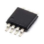
| 封装/外壳 | 8-TSSOP,8-MSOP(0.118",3.00mm 宽) |
| 封装/箱体 | MSOP-8 |
| 工作温度范围 | - 40 C to + 85 C |
| 工作电源电压 | 2.7 V to 5.5 V |
| 工厂包装数量 | 50 |
| 带宽 | 0.1 GHz to 2.5 GHz |
| 最小工作温度 | - 40 C |
| 标准包装 | 1 |
| 电压-电源 | 2.7 V ~ 5.5 V |
| 电流-电源 | 13.7mA |
| 电源电流 | 13.7 mA |
| 类型 | Log Amp Detector |
| 精度 | ±1dB |
| 系列 | AD8313 |
| 视频文件 | http://www.digikey.cn/classic/video.aspx?PlayerID=1364138032001&width=640&height=505&videoID=2245193150001 |
| 输入电压范围—最大 | 5.5 V |
| 输入范围 | -65dBm ~ 0dBm |
| 通道数量 | 1 Channel |
| 频率 | 100MHz ~ 2.5GHz |


- 商务部:美国ITC正式对集成电路等产品启动337调查
- 曝三星4nm工艺存在良率问题 高通将骁龙8 Gen1或转产台积电
- 太阳诱电将投资9.5亿元在常州建新厂生产MLCC 预计2023年完工
- 英特尔发布欧洲新工厂建设计划 深化IDM 2.0 战略
- 台积电先进制程称霸业界 有大客户加持明年业绩稳了
- 达到5530亿美元!SIA预计今年全球半导体销售额将创下新高
- 英特尔拟将自动驾驶子公司Mobileye上市 估值或超500亿美元
- 三星加码芯片和SET,合并消费电子和移动部门,撤换高东真等 CEO
- 三星电子宣布重大人事变动 还合并消费电子和移动部门
- 海关总署:前11个月进口集成电路产品价值2.52万亿元 增长14.8%


PDF Datasheet 数据手册内容提取
0.1 GHz to 2.5 GHz 70 dB Logarithmic Detector/Controller Data Sheet AD8313 FEATURES FUNCTIONAL BLOCK DIAGRAM Wide bandwidth: 0.1 GHz to 2.5 GHz min NINE DETECTOR CELLS + + + + High dynamic range: 70 dB to ±3.0 dB + I→V 8 VOUT High accuracy: ±1.0 dB over 65 dB range (@ 1.9 GHz) VPOS 1 Fast response: 40 ns full-scale typical CINT INHI 2 Controller mode with error output 8dB 8dB 8dB 8dB LP V→I 7 VSET INLO 3 Scaling stable over supply and temperature EIGHT 8dB 3.5GHz AMPLIFIER STAGES Wide supply range: 2.7 V to 5.5 V Low power: 40 mW at 3 V AD8313 INCTOENRTCREOPLT 6 COMM Power-down feature: 60 mW at 3 V CAoPmPpLlIeCteA aTnIdO eNaSsy to use VPOS 4 COSLNOTRPEOL RBEAFNEDR EGNACPE GBIAAISN 5 PWDN 01085-C-001 Figure 1. RF transmitter power amplifier setpoint control and level monitoring Logarithmic amplifier for RSSI measurement cellular base stations, radio link, radar GENERAL DESCRIPTION The AD8313 is a complete multistage demodulating logarithmic Table 1. Next Generation Upgrades for AD8313 amplifier that can accurately convert an RF signal at its input to Part Number Comments an equivalent decibel-scaled value at its dc output. The AD8313 ADL5513 Improved range and temperature stability, maintains a high degree of log conformance for signal frequencies operation up to 4 GHz from 0.1 GHz to 2.5 GHz. Application is straightforward, AD8318 Improved temperature stability, operation up requiring only a single supply of 2.7 V to 5.5 V and the addition to 8 GHz of a suitable input and supply decoupling. Operating on a 3 V AD8317 Lower input range, improved temperature stability, operation up to 10 GHz supply, its 13.7 mA consumption (for T = 25°C) is only 41 mW. A AD8319 Lower input range, improved temperature A power-down feature is provided; the input is taken high to stability, operation up to 10 GHz initiate a low current (20 µA) sleep mode, with a threshold at half the supply voltage. 2.0 5 The AD8313 is fabricated on Analog Devices, Inc., advanced FREQUENCY = 1.9GHz 1.8 4 25 GHz silicon bipolar IC process and is available in an 8-lead 1.6 3 MSOP package. The operating temperature range is −40°C to C) +85°C. V D1.4 2 dB) AGE (1.2 1 ROR ( PUT VOLT10..08 0–1 UTPUT ER UT0.6 –2 O O 0.4 –3 0.2 –4 0–80 –70 –60INPU–T5 A0MPLI–T4U0DE (d–B30m) –20 –10 0–5 01085-C-002 Figure 2. Typical Logarithmic Response and Error vs. Input Amplitude Rev. E Document Feedback Information furnished by Analog Devices is believed to be accurate and reliable. However, no responsibility is assumed by Analog Devices for its use, nor for any infringements of patents or other One Technology Way, P.O. Box 9106, Norwood, MA 02062-9106, U.S.A. rights of third parties that may result from its use. Specifications subject to change without notice. No license is granted by implication or otherwise under any patent or patent rights of Analog Devices. Tel: 781.329.4700 ©1998–2015 Analog Devices, Inc. All rights reserved. Trademarks and registered trademarks are the property of their respective owners. Technical Support www.analog.com
AD8313 Data Sheet TABLE OF CONTENTS Features .............................................................................................. 1 Basic Connections for Log (RSSI) Mode ................................ 15 Applications ....................................................................................... 1 Operating in Controller Mode ................................................. 15 Functional Block Diagram .............................................................. 1 Input Coupling ........................................................................... 16 General Description ......................................................................... 1 Narrow-Band LC Matching Example at 100 MHz ................ 16 Revision History ............................................................................... 2 Adjusting the Log Slope............................................................. 18 Specifications ..................................................................................... 3 Increasing Output Current........................................................ 18 Absolute Maximum Ratings ............................................................ 6 Effect of Waveform Type on Intercept .................................... 19 ESD Caution .................................................................................. 6 Evaluation Board ............................................................................ 20 Pin Configuration and Function Description .............................. 7 Schematic and Layout ................................................................ 20 Typical Performance Characteristics ............................................. 8 General Operation ..................................................................... 20 Circuit Description ......................................................................... 11 Using the AD8009 Operational Amplifier .............................. 20 Interfaces .......................................................................................... 13 Varying the Logarithmic Slope ................................................. 20 Power-Down Interface, PWDN ................................................ 13 Operating in Controller Mode ................................................. 20 Signal Inputs, INHI, INLO ........................................................ 13 RF Burst Response ..................................................................... 20 Logarithmic/Error Output, VOUT .......................................... 13 Outline Dimensions ....................................................................... 24 Setpoint Interface, VSET ........................................................... 14 Ordering Guide .......................................................................... 24 Applications Information .............................................................. 15 REVISION HISTORY 9/15—Rev. D to Rev. E Changes to General Description Section ...................................... 1 Added Table 1; Renumbered Sequentially .................................... 1 Updated Outline Dimensions ....................................................... 24 Changes to Ordering Guide .......................................................... 24 6/04—Rev. C to Rev. D Updated Evaluation Board Section .............................................. 21 2/03—Rev. B to Rev. C TPCs and Figures Renumbered ........................................ Universal Edits to Specifications ...................................................................... 2 Updated ESD Caution ...................................................................... 4 Updated Outline Dimensions ......................................................... 7 8/99—Rev. A to Rev. B 5/99—Rev. 0 to Rev. A 8/98—Revision 0: Initial Version Rev. E | Page 2 of 24
Data Sheet AD8313 SPECIFICATIONS T = 25°C, V = 5 V1, R = 10 kΩ, unless otherwise noted. A S L Table 2. Parameter Test Conditions/Comments Min2 Typ Max2 Unit SIGNAL INPUT INTERFACE Specified Frequency Range 0.1 2.5 GHz DC Common-Mode Voltage V – 0.75 V POS Input Bias Currents 10 µA Input Impedance f < 100 MHz3 900||1.1 Ω||pF4 RF LOG (RSSI) MODE Sinusoidal, input termination configuration shown in Figure 29 100 MHz5 Nominal conditions ±3 dB Dynamic Range6 53.5 65 dB Range Center −31.5 dBm ±1 dB Dynamic Range 56 dB Slope 17 19 21 mV/dB Intercept −96 −88 −80 dBm 2.7 V ≤ V ≤ 5.5 V, −40°C ≤ T ≤ +85°C S ±3 dB Dynamic Range 51 64 dB Range Center −31 dBm ±1 dB Dynamic Range 55 dB Slope 16 19 22 mV/dB Intercept −99 −89 −75 dBm Temperature Sensitivity P = −10 dBm −0.022 dB/°C IN 900 MHz5 Nominal conditions ±3 dB Dynamic Range 60 69 dB Range Center −32.5 dBm ±1 dB Dynamic Range 62 dB Slope 15.5 18 20.5 mV/dB Intercept −105 −93 −81 dBm 2.7 V ≤ V ≤ 5.5 V, –40°C ≤ T ≤ +85°C S ±3 dB Dynamic Range 55.5 68.5 dB Range Center –32.75 dBm ±1 dB Dynamic Range 61 dB Slope 15 18 21 mV/dB Intercept –110 –95 –80 dBm Temperature Sensitivity P = –10 dBm –0.019 dB/°C IN 1.9 GHz7 Nominal conditions ±3 dB Dynamic Range 52 73 dB Range Center –36.5 dBm ±1 dB Dynamic Range 62 dB Slope 15 17.5 20.5 mV/dB Intercept –115 –100 –85 dBm 2.7 V ≤ V ≤ 5.5 V, –40°C ≤ T ≤ +85°C S ±3 dB Dynamic Range 50 73 dB Range Center –36.5 dBm ±1 dB Dynamic Range 60 dB Slope 14 17.5 21.5 mV/dB Intercept –125 –101 –78 dBm Temperature Sensitivity P = –10 dBm –0.019 dB/°C IN Rev. E | Page 3 of 24
AD8313 Data Sheet Parameter Test Conditions/Comments Min2 Typ Max2 Unit 2.5 GHz7 Nominal conditions ±3 dB Dynamic Range 48 66 dB Range Center –34 dBm ±1 dB Dynamic Range 46 dB Slope 16 20 25 mV/dB Intercept –111 –92 –72 dBm 2.7 V ≤ V ≤ 5.5 V, –40°C ≤ T ≤ +85°C S ±3 dB Dynamic Range 47 68 dB Range Center –34.5 dBm ±1 dB Dynamic Range 46 dB Slope 14.5 20 25 mV/dB Intercept –128 –92 –56 dBm Temperature Sensitivity P =–10 dBm –0.040 dB/°C IN 3.5 GHz5 Nominal conditions ±3 dB Dynamic Range 43 dB ±1 dB Dynamic Range 35 dB Slope 24 mV/dB Intercept –65 dBm CONTROL MODE Controller Sensitivity f = 900 MHz 23 V/dB Low Frequency Gain VSET to VOUT8 84 dB Open-Loop Corner Frequency VSET to VOUT8 700 Hz Open-Loop Slew Rate f = 900 MHz 2.5 V/µs VSET Delay Time 150 ns VOUT INTERFACE Current Drive Capability Source Current 400 µA Sink Current 10 mA Minimum Output Voltage Open-loop 50 mV Maximum Output Voltage Open-loop V – 0.1 V POS Output Noise Spectral Density P = –60 dBm, f = 100 Hz 2.0 µV/√Hz IN SPOT P = –60 dBm, f = 10 MHz 1.3 µV/√Hz IN SPOT Small Signal Response Time P = –60 dBm to –57 dBm, 10% to 90% 40 60 ns IN Large Signal Response Time P = No signal to 0 dBm; settled to 0.5 dB 110 160 ns IN VSET INTERFACE Input Voltage Range 0 V V POS Input Impedance 18||1 kΩ||pF4 POWER-DOWN INTERFACE PWDN Threshold V /2 V POS Power-Up Response Time Time delay following high to low transition 1.8 µs until device meets full specifications. PWDN Input Bias Current PWDN = 0 V 5 µA PWDN = V <1 µA S Rev. E | Page 4 of 24
Data Sheet AD8313 Parameter Test Conditions/Comments Min2 Typ Max2 Unit POWER SUPPLY Operating Range 2.7 5.5 V Powered-Up Current 13.7 15.5 mA 4.5 V ≤V ≤ 5.5 V, –40°C ≤ T ≤ +85°C 18.5 mA S 2.7 V ≤V ≤ 3.3 V, –40°C ≤ T ≤ +85°C 18.5 mA S Powered-Down Current 4.5 V ≤V ≤ 5.5 V, –40°C ≤ T ≤ +85°C 50 150 µA S 2.7 V ≤V ≤ 3.3 V, –40°C ≤ T ≤ +85°C 20 50 µA S 1 Except where otherwise noted; performance at VS = 3 V is equivalent to 5 V operation. 2 Minimum and maximum specified limits on parameters that are guaranteed but not tested are 6 sigma values. 3 Input impedance shown over frequency range in Figure 26. 4 Double vertical bars (||) denote “in parallel with.” 5 Linear regression calculation for error curve taken from –40 dBm to –10 dBm for all parameters. 6 Dynamic range refers to range over which the linearity error remains within the stated bound. 7 Linear regression calculation for error curve taken from –60 dBm to –5 dBm for 3 dB dynamic range. All other regressions taken from –40 dBm to –10 dBm. 8 AC response shown in Figure 12. Rev. E | Page 5 of 24
AD8313 Data Sheet ABSOLUTE MAXIMUM RATINGS Stresses at or above those listed under Absolute Maximum Table 3. Ratings may cause permanent damage to the product. This is a Parameter Rating stress rating only; functional operation of the product at these Supply Voltage V 5.5 V S or any other conditions above those indicated in the operational VOUT, VSET, PWDN 0 V, VPOS section of this specification is not implied. Operation beyond Input Power Differential (re: 50 Ω, 5.5 V) 25 dBm the maximum operating conditions for extended periods may Input Power Single-Ended (re: 50 Ω, 5.5 V) 19 dBm affect product reliability. Internal Power Dissipation 200 mW θ 200°C/W JA ESD CAUTION Maximum Junction Temperature 125°C Operating Temperature Range –40°C to +85°C Storage Temperature Range –65°C to +150°C Rev. E | Page 6 of 24
Data Sheet AD8313 PIN CONFIGURATION AND FUNCTION DESCRIPTION VPOS 1 8 VOUT AD8313 INHI 2 7 VSET VIPNOLOS 34 (NToOt Pto V SIEcaWle) 65 CPWOMDMN 01085-C-003 Figure 3. Pin Configuration Table 4. Pin Function Descriptions Pin No. Mnemonic Description 1, 4 VPOS Positive Supply Voltage (VPOS), 2.7 V to 5.5 V. 2 INHI Noninverting Input. This input should be ac-coupled. 3 INLO Inverting Input. This input should be ac-coupled. 5 PWDN Connect Pin to Ground for Normal Operating Mode. Connect this pin to the supply for power-down mode. 6 COMM Device Common. 7 VSET Setpoint Input for Operation in Controller Mode. To operate in RSSI mode, short VSET and VOUT. 8 VOUT Logarithmic/Error Output. Rev. E | Page 7 of 24
AD8313 Data Sheet TYPICAL PERFORMANCE CHARACTERISTICS T = 25°C, V = 5 V, R input match shown in Figure 29, unless otherwise noted. A S L 2.0 2.0 5 1.8 1.8 4 1.6 1.6 3 1.4 1.4 2 100MHz (V)OUT11..20 1.9GHz 2.5GHz (V)OUT11..20 –+4205°°CC 10 ROR (dB) V V R 0.8 0.8 –1 E +85°C 0.6 0.6 –2 0.4 900MHz 0.4 –3 SLOPE AND INTERCEPT NORMALIZED AT +25°C 0.2 0.2 –4 AND APPLIED TO–40°C AND +85°C 0–70 –60 –50INPU–T4 A0MPLI–T3U0DE (d–B20m) –10 0 10 01085-C-004 0–70 –60 –50 INP–U4T0 AMP–L3IT0UDE –(2d0Bm)–10 0 10–5 01-85-C-007 Figure 4. VOUT vs. Input Amplitude Figure 7. VOUT and Log Conformance vs. Input Amplitude at 900 MHz for Multiple Temperatures 6 2.0 5 1.8 4 4 1.6 3 900MHz –40°C 1.4 2 2 100MHz ERROR (dB) 0 2.5GHz 900MHz V (V)OUT110...208 ++8255°°CC 10–1 ERROR (dB) –2 1.9GHz 2.5GHz 100MHz 0.6 –2 1.9GHz 0.4 –3 –4 SLOPE AND INTERCEPT NORMALIZED AT +25°C 0.2 –4 AND APPLIED TO–40°C AND +85°C –6–70 –60 –50INPU–T4 A0MPLI–T3U0DE (d–B2m0) –10 0 10 01085-C-005 0–70 –60 –50 INP–U4T0 AMP–L3IT0UDE –(2d0Bm)–10 0 10–5 01085-C-008 Figure 5. Log Conformance vs. Input Amplitude Figure 8. VOUT and Log Conformance vs. Input Amplitude at 1.9 GHz for Multiple Temperatures 2.0 5 2.0 5 1.8 4 1.8 4 1.6 3 1.6 3 –40°C 1.4 2 1.4 2 1.2 –40°C 1 B) 1.2 1 B) V (V)OUT1.0 ++8255°°CC 0 RROR (d V (V)OUT1.0 +25°C 0 RROR (d 0.8 –1 E 0.8 –1 E SLOPE AND INTERCEPT 0.6 –2 0.6 NORMALIZED AT +25°C AND –2 APPLIED TO–40°C AND +85°C 0.4 –3 0.4 –3 0.2 SLOPE AND INTERCEPT NORMALIZED AT +25°C –4 0.2 +85°C –4 AND APPLIED TO–40°C AND +85°C 0–70 –60 –50INPU–T4 A0MPLI–T3U0DE (d–B20m) –10 0 10–5 01085-C-006 0–70 –60 –50 INP–U4T0 AMP–L3IT0UDE– (2d0Bm)–10 0 10–5 01085-C-009 Figure 6. VOUT and Log Conformance vs. Input Amplitude at 100 MHz for Figure 9. VOUT and Log Conformance vs. Input Amplitude at 2.5 GHz for Multiple Temperatures Multiple Temperatures Rev. E | Page 8 of 24
Data Sheet AD8313 22 –70 21 –80 +85°C SLOPE (mV/dB)211098 –40°+C25°C INTERCEPT (dBm)–90 +25°C+85°C –100 17 –40°C 160 500 FR1E0Q00UENCY (M15H0z0) 2000 2500 01085-C-010 –1100 500 FR10E0Q0UENCY (1M5H00z) 2000 2500 01085-C-013 Figure 10. VOUT Slope vs. Frequency for Multiple Temperatures Figure 13. VOUT Intercept vs. Frequency for Multiple Temperatures 24 –70 23 –75 SPECIFIED OPERATING RANGE 22 SPECIFIED OPERATING RANGE –80 21 SLOPE (mV/dB)211098 2.5GHz100MHz 900MHz NTERCEPT (dBm) –––899505 920.50GMHHzz 100MHz 17 1.9GHz I 1.9GHz –100 16 –105 15 142.5 3.0 3.5 SUPP4L.Y0 VOLT4A.5GE (V)5.0 5.5 6.0 01085-C-011 –1102.5 3.0 3.5SUPP4L.Y0 VOLT4A.G5E (V)5.0 5.5 6.0 01085-C-014 Figure 11. VOUT Slope vs. Supply Voltage Figure 14. VOUT Intercept vs. Supply Voltage REF LEVEL = 92dB 10 2GHz RF INPUT SCALE: 10dB/DIV RF INPUT –70dBm B) –60dBm d N ( GAIOUT µV/ Hz 1 ––5550ddBBmm V O TT –45dBm E S V –40dBm –35dBm –30dBm 100 1k FREQUEN1C0Yk (Hz) 100k 1M 01085-C-012 0.1100 1k F1R0EkQUENCY1 (0H0zk) 1M 10M 01085-C-015 Figure 12. AC Response from VSET to VOUT Figure 15. VOUT Noise Spectral Density Rev. E | Page 9 of 24
AD8313 Data Sheet 100.00 CH. 1 AND CH. 2: 200mV/DIV AVERAGE: 50 SAMPLES 13.7mA VS = +5.5V CH. 1 10.00 mA) VS = +2.7V T ( CH. 2 N E R PULSED RF UR 1.00 CH. 1 GND 100MHz,–45dBm C LY VPOS = +3V VPOS = +5V CH. 2 GND P P U S 0.10 0.010 1 PWD2N VOLTAGE3 2(V0)µA 4 40µA5 01085-C-016 HORIZONTAL: 50ns/DIV 01085-C-019 Figure 16. Typical Supply Current vs. PWDN Voltage Figure 18. Response Time, No Signal to –45 dBm CH. 1 AND CH. 2: 1V/DIV CH. 3: 5V/DIV CH.1&CH.2:500mV/DIV AVERAGE:50SAMPLES VOUT @ VS = +5.5V VS = +5.5V CH.1 CH. 1 GND VS = +2.7V CH.2 VOUT @ CH. 1 GND VS = +2.7V CH. 2 GND CH. 2 GND PULSED RF 100MHz,0dBm PWDN CH. 3 GND HORIZONTAL: 1µs/DIV 01085-C-017 HORIZONTAL:50ns/DIV 01085-C-020 Figure 17. PWDN Response Time Figure 19. Response Time, No Signal to 0 dBm HP8648B 10MHz REF OUTPUT EXT TRIG HP8112A OUT HP8648B GESNIEGRNAATRLOFR OUT PIN = 0dBm GENPEURLSAETOR GESNPIEUGRLNSAAETLOR 1P0UMLHSzE RMEOFD OEU ITNPUT EXT TROIUGT GEHNPPEU8RL11SA2ETAOR TORUITG MODULATION 0+.V0S1µF10Ω 0.1µF 1 VPAODS83V1O3UT 8 FTEETK P PR6O20B5E TSDCTSEO7K8P4EC TRIG MODERF OUT 2 INHI VSET 7 RF –6dB 0.01µF 54.9Ω 0603 SIZE SURFACE SPLITTER +VS 10Ω 0.1µF 34 IVNPLOOS CPOWMDMN 65 MA OLUONWT L CEOAMKPAOGNEE PNCT SB OOANRD 01085-C-018 –6dB 0+.V0S10µ.0F110µΩF 05.14µ.9FΩ12 IVNPAHOIDS83VV1OS3EUTT 87 FTE0E6TK0 P 3PR S6O2IZ0BE5E SURFTASDCCTSEEO7K8P4EC TRIG Figure 20. Test Setup for PWDN Response Time 3 INLO COMM 6 MOUNT COMPONENTS ON A LOW LEAKAGE PC BOARD +VS 10Ω 0.1µF 4 VPOS PWDN 5 01085-C-021 Figure 21. Test Setup for RSSI Mode Pulse Response Rev. E | Page 10 of 24
Data Sheet AD8313 CIRCUIT DESCRIPTION The AD8313 is an 8-stage logarithmic amplifier, specifically capacity of the first detector cell, and occurs at approximately designed for use in RF measurement and power amplifier 0 dBm. The practical dynamic range is over 70 dB to the ±3 dB control applications at frequencies up to 2.5 GHz. A block error points. However, some erosion of this range can occur at diagram is shown in Figure 22. For a detailed description of temperature and frequency extremes. Useful operation to over log amp theory and design principles, refer to the AD8307 3 GHz is possible, and the AD8313 remains serviceable at data sheet. 10 MHz, needing only a small amount of additional ripple filtering. NINE DETECTOR CELLS + + + + + I→V 8 VOUT 2.0 5 VPOS 1 1.8 SLOPE = 18mV/dB 4 CINT 1.6 3 INHI 2 INLO 3 8dB 8dB 8dB 8dB LP V→I 7 VSET 1.4 2 EIGHT 8dB 3.5GHz AMPLIFIER STAGES 1.2 1 B) AD8313 INCTOENRTCREOPLT 6 COMM (V)OUT1.0 0 ROR (d V R 0.8 –1 E VPOS 4 COSLNOTPREOL RBEAFNEDR EGNACPE GBAIAINS 5 PWDN 01085-C-001 00..64 ––23 Figure 22. Block Diagram INTERCEPT =–100dBm 0.2 –4 A(P ifnusll y2 danifdfe 3re)n atriea li ndteesringnal liys ubsiaesde.d I ntop uatpsp IrNoxHimI aantedl yI N0.L7O5 V 0–90 –80 –70 INP–U60T AM–P5L0ITUD–4E0 (dBm–3)0 –20 –10 0–5 01085-c-023 below the supply voltage, and present a low frequency impedance Figure 23. Typical RSSI Response and Error vs. Input Power at 1.9 GHz of nominally 900 Ω in parallel with 1.1 pF. The noise spectral The fluctuating current output generated by the detector cells, density referred to the input is 0.6 nV/√Hz, equivalent to a with a fundamental component at twice the signal frequency, is voltage of 35 V rms in a 3.5 GHz bandwidth, or a noise power filtered first by a low-pass section inside each cell, and then by of −76 dBm re: 50 Ω. This sets the lower limit to the dynamic the output stage. The output stage converts these currents to a range; the Applications section shows how to increase the voltage, V , at VOUT (Pin 8), which can swing rail-to-rail. sensitivity by using a matching network or input transformer. OUT The filter exhibits a 2-pole response with a corner at However, the low end accuracy of the AD8313 is enhanced by approximately 12 MHz and full-scale rise time (10% to 90%) of specially shaping the demodulation transfer characteristic to 40 ns. The residual output ripple at an input frequency of partially compensate for errors due to internal noise. 100 MHz has an amplitude of under 1 mV. The output can drive Each of the eight cascaded stages has a nominal voltage gain of a small resistive load; it can source currents of up to 400 µA, 8 dB and a bandwidth of 3.5 GHz. Each stage is supported by and sink up to 10 mA. The output is stable with any capacitive precision biasing cells that determine this gain and stabilize it load, though settling time could be impaired. The low against supply and temperature variations. Since these stages are frequency incremental output impedance is approximately direct-coupled and the dc gain is high, an offset compensation 0.2 Ω. loop is included. The first four stages and the biasing system are In addition to its use as an RF power measurement device (that powered from Pin 4, while the later stages and the output inter- is, as a logarithmic amplifier), the AD8313 may also be used in faces are powered from Pin 1. The biasing is controlled by a logic controller applications by breaking the feedback path from interface PWDN (Pin 5); this is grounded for normal operation, VOUT to VSET (Pin 7), which determines the slope of the but may be taken high (to V) to disable the chip. The threshold S output (nominally 18 mV/dB). This pin becomes the setpoint is at V /2 and the biasing functions are enabled and disabled POS input in controller modes. In this mode, the voltage V within 1.8 µs. OUT remains close to ground (typically under 50 mV) until the Each amplifier stage has a detector cell associated with its decibel equivalent of the voltage V is reached at the input, SET output. These nonlinear cells perform an absolute value (full- when V makes a rapid transition to a voltage close to V OUT POS wave rectification) function on the differential voltages along (see the Operating in Controller Mode section). The logarithmic this backbone in a transconductance fashion; their outputs are intercept is nominally positioned at −100 dBm (re: 50 Ω); this is in current-mode form and are thus easily summed. A ninth effective in both the log amp mode and the controller mode. detector cell is added at the input of the AD8313. Since the midrange response of each of these nine detector stages is separated by 8 dB, the overall dynamic range is about 72 dB (Figure 23). The upper end of this range is determined by the Rev. E | Page 11 of 24
AD8313 Data Sheet With Pins 7 and 8 connected (log amp mode), the output can be With Pins 7 and 8 disconnected (controller mode), the output stated as can be stated as V =V (P +100dBm) V →V when V log(P /100)>V OUT SLOPE IN OUT S SLOPE IN SET where PIN is the input power stated in dBm when the source is VOUT →0 when VSLOPE log(PIN /100)<VSET directly terminated in 50 Ω. However, the input impedance of when the input is stated in terms of the power of a sinusoidal the AD8313 is much higher than 50 Ω, and the sensitivity of this signal across a net termination impedance of 50 Ω. The transition device may be increased by about 12 dB by using some type of zone between high and low states is very narrow since the output matching network (see below), which adds a voltage gain and stage behaves essentially as a fast integrator. The above equations lowers the intercept by the same amount. Dependence on the ref- can be restated as erence impedance can be avoided by restating the expression as V →V when V log(V /2.2µV)>V V =20×V ×log×(V /2.2µV) OUT S SLOPE IN SET OUT SLOPE IN V →0 when V log(V /2.2µV)<V where V is the rms value of a sinusoidal input appearing OUT SLOPE IN SET IN across Pins 2 and 3; here, 2.2 µV corresponds to the intercept, Another use of the separate VOUT and VSET pins is in raising expressed in voltage terms. For detailed information on the the load-driving current capability by including an external effect of signal waveform and metrics on the intercept NPN emitter follower. More complete information about usage positioning for a log amp, refer to the AD8307 data sheet. in these modes is provided in the Applications section. Rev. E | Page 12 of 24
Data Sheet AD8313 INTERFACES This section describes the signal and control interfaces and For high frequency use, Figure 26 shows the input impedance their behavior. On-chip resistances and capacitances exhibit plotted on a Smith chart. This measured result of a typical variations of up to ±20%. These resistances are sometimes device includes a 191 mil 50 Ω trace and a 680 pF capacitor to temperature-dependent, and the capacitances may be voltage- ground from the INLO pin. dependent. POWER-DOWN INTERFACE, PWDN Frequency R +jX 100MHz 100MHz 650–j400 900MHz 55 –j135 The power-down threshold is accurately centered at the 1.9GHz 22 –j65 2.5GHz 23 –j43 AD8313 MEASURED midpoint of the supply as shown in Figure 24. If Pin 5 is left unconnected or tied to the supply voltage (recommended), the 900MHz bias enable current is shut off, and the current drawn from the supply is predominately through a nominal 300 kΩ chain 2.5GHz (T2h0e µ tAhr aets h3o Vld) .l eWvehle ins agcrcouurnadteeldy, atth Ve PbOiSa/s2 s. yWsthemen ios ptuerranteidn go inn. 1.9GHz 900Ω 1.1pF 01085-C-026 the device ON state, the input bias current at the PWDN pin is Figure 26. Typical Input Impedance approximately 5 µA for V = 3 V. POS LOGARITHMIC/ERROR OUTPUT, VOUT VPOS 4 The rail-to-rail output interface is shown in Figure 27. V can 50kΩ 150kΩ OUT run from within about 50 mV of ground, to within about 100 mV 75kΩ TO BIAS of the supply voltage, and is short-circuit safe to either supply. PWDN 5 ENABLE However, the sourcing load current, I , is limited to that SOURCE which is provided by the PNP transistor, typically 400 µA. Larger load currents can be provided by adding an external NPN COMM 6 150kΩ 01085-C-024 torfa tnhsiiss taomr p(sliefeie trh ies Ahipgphl,i caantido ints m seacyt iboen r)e. gTahrde eddc aosp aenn -ilnotoegpr gaatoinr Figure 24. Power-Down Threshold Circuitry having a capacitance of 2 pF (C ) driven by the current-mode INT SIGNAL INPUTS, INHI, INLO signal generated by the summed outputs of the nine detector stages, which is scaled approximately 4.0 µA/dB. The simplest low frequency ac model for this interface consists of just a 900 Ω resistance, R , in shunt with a 1.1 pF input cap- 1 VPOS IN acitance, C , connected across INHI and INLO. Figure 25 shows BIAS IN ISOURCE these distributed in the context of a more complete schematic. SETPFOROINMT gmSTAGE 400µA VOUT The input bias voltage shown is for the enabled chip; when SUMMED CINT 8 LP disabled, it rises by a few hundred millivolts. If the input is DETECTOR ctthroaeunspesl iecedanp tv aticoai tbcoaerp si anactnirtdoo dRrsuI,Nc .te hFdios, r hc tahhvaiisnn grgee aa ms toianmy, elca acruogsnee sc taoa ulnoptw lfio nlregmv ceealp dsa ibgcynit aolr s OUTPUTS LM 1M0AmXA 6 COMM CL 01085-C-027 Figure 27. Output Interface Circuitry should be well matched. This is not necessary when using the small capacitors found in many impedance transforming Thus, for midscale RF input of about 3 mV, which is some 40 networks used at high frequencies. dB above the minimum detector output, this current is 160 µA, VPOS 1 TO STAGES and the output changes by 8 V/µs. When VOUT is connected to 1 TO 4 0.5pF ~0.75V 125Ω 125Ω VSET, the rise and fall times are approximately 40 ns (for RL ≥ 10 kΩ). 2.5kΩ 2.5kΩ 1.25kΩ TO 2ND INHI 2 STAGE The nominal slew rate is 2.5 V/µs. The HF compensation tech- 0.7pF INLO 3 nique results in stable operation with a large capacitive load, CL, though the positive-going slew rate is then limited by I /C 1.25kΩ SOURCE L 0.5pF GAIN BIAS to 1 V/µs for C = 400 pF. L (1ST DETECTOR) 1.24V VPOS 4 250Ω ~1.4mA COMM 01085-C-025 Figure 25. Input Interface Simplified Schematic Rev. E | Page 13 of 24
AD8313 Data Sheet SETPOINT INTERFACE, VSET VPOS 1 25µA 25µA TFOD BOK/P The setpoint interface is shown in Figure 28. The voltage, V , SET R1 STAGE is divided by a factor of 3 in a resistive attenuator of 18 kΩ total 12kΩ VSET 8 LP resistance. The signal is converted to a current by the action of the op amp and the resistor R3 (1.5 kΩ), which balances the R2 current generated by the summed output of the nine detector 6kΩ cneolmls ianta tlhlye 3in µpsu ×t t4o. 0th µeA p/rdeBv i×o u1s. 5c eklΩl. T=h 1e8 l omgVar/idthBm. ic slope is COMM 6 1.5kRΩ3 01085-C-028 Figure 28. Setpoint Interface Circuitry Rev. E | Page 14 of 24
Data Sheet AD8313 APPLICATIONS INFORMATION BASIC CONNECTIONS FOR LOG (RSSI) MODE OPERATING IN CONTROLLER MODE Figure 29 shows the AD8313 connected in its basic measurement Figure 30 shows the basic connections for operation in controller mode. A power supply between 2.7 V and 5.5 V is required. The mode. The link between VOUT and VSET is broken and a set- power supply to each of the VPOS pins should be decoupled point is applied to VSET. Any difference between V and the SET with a 0.1 µF surface-mount ceramic capacitor and a 10 Ω series equivalent input power to the AD8313 drives V either to the OUT resistor. supply rail or close to ground. If V is greater than the SET equivalent input power, V is driven toward ground, and vice The PWDN pin is shown as grounded. The AD8313 may be OUT versa. disabled by a logic high at this pin. When disabled, the chip current is reduced to about 20 µA from its normal value of R1 10Ω RPROT 13.7 mA. The logic threshold is at VPOS/2, and the enable +VS 0.1µF 1 VPAODS83V1O3UT 8 function occurs in about 1.8 µs. However, that additional 2 INHI VSET 7 settling time is generally needed at low input levels. While the input in this case is terminated with a simple 50 Ω broadband 3 INLO COMM 6 R3 rnCeaostiuisoptnilvi nec agmn s aebtcect hiao,c ntch.o emrep alirseh meda. nTyh wesaey sa rien dwishciuchss tehde i nin tphuet Itneprmuti - Figu+rVeS 30. Ba10siΩc Con0n.e1µcFtions 4forV OPOpSeraPtWioDnN in5 the Controller 01085-C-030Mo de VSET is connected to VOUT to establish a feedback path that This mode of operation is useful in applications where the output controls the overall scaling of the logarithmic amplifier. The power of an RF power amplifier (PA) is to be controlled by an load resistance, RL, should not be lower than 5 kΩ so that the analog AGC loop (Figure 31). In this mode, a setpoint voltage, full-scale output of 1.75 V can be generated with the limited proportional in dB to the desired output power, is applied to the available current of 400 µA max. VSET pin. A sample of the output power from the PA, via a As stated in the Absolute Maximum Ratings table, an externally directional coupler or other means, is fed to the input of the applied overvoltage on the VOUT pin, which is outside the AD8313. range 0 V to VPOS, is sufficient to cause permanent damage to ENVELOPE OF TRANSMITTED the device. If overvoltages are expected on the VOUT pin, a SIGNAL series resistor, R , should be included as shown. A 500 Ω PROT resistor is sufficient to protect against overvoltage up to ±5 V; POWER AMPLIFIER 1000 Ω should be used if an overvoltage of up to ±15 V is RF IN expected. Since the output stage is meant to drive loads of no DIRECTIONAL more than 400 µA, this resistor does not impact device COUPLER performance for higher impedance drive applications (higher AD8313 output current applications are discussed in the Increasing VOUT Output Current section). RFIN VSET SETPOINT +VS680pF1R01Ω 0.1µF 1 VPAODS83V1O3UT 8 RPROT RL= 1MΩ CONTROL DAC 01085-C-031 2 INHI VSET 7 Figure 31. Setpoint Controller Operation 680pF 53.6Ω R2 3 INLO COMM 6 VOUT is applied to the gain control terminal of the power +VS 10Ω 0.1µF 4 VPOS PWDN 5 01085-C-029 aavmmoltppallgiiffeii eedrr.e scThrhoeeau slgdeas ib ngea ciaonnn. it nrovle rtrsaen rsefleart ifounnschtiipo,n t hoaf tt hise, ipnocwreears ing Figure 29. Basic Connections for Log (RSSI) Mode A positive input step on V (indicating a demand for increased SET power from the PA) drives V toward ground. This should be OUT arranged to increase the gain of the PA. The loop settles when V settles to a voltage that sets the input power to the AD8313 OUT to the dB equivalent of V . SET Rev. E | Page 15 of 24
AD8313 Data Sheet INPUT COUPLING 3 The signal can be coupled to the AD8313 in a variety of ways. BALANCED 2 In all cases, there must not be a dc path from the input pins to ground. Some of the possibilities include dual-input coupling TERMINATED 1 capacitors, a flux-linked transformer, a printed circuit balun, B) MATCHED DR = 66dB d direct drive from a directional coupler, or a narrow-band OR (0 impedance matching network. R R E BALANCED Figure 32 shows a simple broadband resistive match. A –1 DR = 71dB termination resistor of 53.6 Ω combines with the internal input impedance of the AD8313 to give an overall resistive input –2 MATCHED DR = 69dB impedance of approximately 50 Ω. It is preferable to place the tIeNrLmOin, awtihoenr er eits ilsotwore rdsi rtehcet lpyo ascsribolses dthelee tinerpiuotu ps ienfsfe, cItNs HofI dtoc –3–90 –80 –70 –6IN0PUT–5 A0MP–L4IT0UD–E3 (0dBm–2)0 –10 0 10 01085-C-033 offset voltages on the low end of the dynamic range. At low Figure 33. Comparison of Terminated, Matched, and Balanced Input Drive at 900 MHz frequencies, this may not be quite as beneficial, since it requires larger coupling capacitors. The two 680 pF input coupling 3 capacitors set the high-pass corner frequency of the network at TERMINATED DR = 75dB 9.4 MHz. 2 MATCHED 50ΩSOURCE C1 AD8313 50Ω 680pF B) 1 TERMINATED d 68C02pF R53M.6AΩTCH CIN RIN 01085-C-032 ERROR (–01 BALANCED DMRA T=C 7H3EdDB Figure 32. A Simple Broadband Resistive Input Termination BALANCED The high-pass corner frequency can be set higher according to –2 DR = 75dB the equation f3dB = 2×π×1C×50 –F3i–g9u0re 3–480. Co–m70par–is6IoN0nPU oT–f5 TA0eMrPm–Li4InT0UatDeE–d3 (,0 dMBam–t)2c0hed–, 1a0nd B0alanc1e0d 01085-C-034 Input Drive at 1.9 GHz where: NARROW-BAND LC MATCHING EXAMPLE C1×C2 C= AT 100 MHz C1×C2 While numerous software programs provide an easy way to In high frequency applications, the use of a transformer, balun, calculate the values of matching components, a clear under- or matching network is advantageous. The impedance matching standing of the calculations involved is valuable. A low frequency characteristics of these networks provide what is essentially a (100 MHz) value has been used for this example because of the gain stage before the AD8313 that increases the device sensitivity. deleterious board effects at higher frequencies. RF layout This gain effect is explored in the following matching example. simulation software is useful when board design at higher Figure 33 and Figure 34 show device performance under these frequencies is required. three input conditions at 900 MHz and 1.9 GHz. A narrow-band LC match can be implemented either as a While the 900 MHz case clearly shows the effect of input series-inductance/shunt-capacitance or as a series-capacitance/ matching by realigning the intercept as expected, little shunt-inductance. However, the concurrent requirement that improvement is seen at 1.9 GHz. Clearly, if no improvement the AD8313 inputs, INHI and INLO, be ac-coupled, makes a in sensitivity is required, a simple 50 Ω termination may be series-capacitance/shunt-inductance type match more the best choice for a given design based on ease of use and appropriate (Figure 35). cost of components. 50ΩSOURCE AD8313 50Ω C1 LMATCH CIN RIN C2 01085-C-035 Figure 35. Narrow-Band Reactive Match Rev. E | Page 16 of 24
Data Sheet AD8313 Typically, the AD8313 needs to be matched to 50 Ω. The input C . Alternatively, C1 and C2 can each be set to twice C MATCH MATCH impedance of the AD8313 at 100 MHz can be read from the so that the total series capacitance is equal to C . By making MATCH Smith chart (Figure 26) and corresponds to a resistive input C1 and C2 slightly unequal (that is, select C2 to be about 10% impedance of 900 Ω in parallel with a capacitance of 1.1 pF. less than C1) but keeping their series value the same, the ampli- tude of the signals on INHI and INLO can be equalized so that To make the matching process simpler, the AD8313 input cap- the AD8313 is driven in a more balanced manner. Any of the acitance, C , can be temporarily removed from the calculation IN options detailed above can be used provided that the combined by adding a virtual shunt inductor (L2), which resonates away series value of C1 and C2, that is, C1 × C2/(C1 + C2) is equal to C (Figure 36). This inductor is factored back into the calculation IN C . later. This allows the main calculation to be based on a simple MATCH resistive-to-resistive match, that is, 50 Ω to 900 Ω. In all cases, the values of C and L must be chosen from MATCH MATCH standard values. At this point, these values need now be installed The resonant frequency is defined by the equation on the board and measured for performance at 100 MHz. 1 ω= Because of board and layout parasitics, the component values L2×C from the preceding example had to be tuned to the final values IN of C = 8.9 pF and L = 270 nH as shown in Table 5. MATCH MATCH therefore, Assuming a lossless matching network and noting conservation 1 L2= =2.3µH of power, the impedance transformation from RS to RIN (50 Ω to ω2CIN 900 Ω) has an associated voltage gain given by 50ΩSOURC5E0Ω C1 AD8313 GaindB=20×log RIN =12.6dB R S C2 (C1L1× C2) L2 CIN RIN 01085-C-036 Bpefoefewccaeturis,v eeth tiehn epv ouAlttD alog8we3 1-ge3an iindn popufo ttw hreeers m pseoanntcsdhitsii nvtoigt yvn obelttywa tgoheri ska n aidnm cnoroeuatn stteo. s Tt trhhuuees , CMATCH=(C1 + C2) TEMPORARY in this case, the dynamic range is shifted downward, that is, the (C1× C2) INDUCTANCE LMATCH=(C1 + C2) 12.6 dB voltage gain shifts the 0 dBm to −65 dBm input range Figure 36. Input Matching Example downward to −12.6 dBm to −77.6 dBm. However, because of With C and L2 temporarily out of the picture, the focus is now network losses, this gain is not be fully realized in practice. IN on matching a 50 Ω source resistance to a (purely resistive) load Refer to Figure 33 and Figure 34 for an example of practical of 900 Ω and calculating values for C and L1. When attainable voltage gains. MATCH L1 Table 5 shows recommended values for the inductor and cap- R R = S IN C acitors in Figure 35 for some selected RF frequencies in addition MATCH to the associated theoretical voltage gain. These values for a the input looks purely resistive at a frequency given by reactive match are optimal for the board layout detailed as 1 Figure 45. f = =100MHz 0 2π L1×CMATCH As previously discussed, a modification of the board layout produces networks that may not perform as specified. At Solving for C gives MATCH 2.5 GHz, a shunt inductor is sufficient to achieve proper 1 1 C = × =7.5pF matching. Consequently, C1 and C2 are set sufficiently high MATCH RSRIN 2πf0 that they appear as RF shorts. Solving for L1 gives Table 5. Recommended Values for C1, C2, and L in MATCH Figure 35 R R L1= S IN =337.6nH Freq. C C1 C2 L Voltage 2πf MATCH MATCH 0 (MHz) (pF) (pF) (pF) (nH) Gain(dB) Because L1 and L2 are parallel, they can be combined to give 100 8.9 22 15 270 12.6 the final value for L , that is, 1000 270 MATCH 900 1.5 3 3 8.2 9.0 L1×L2 LMATCH = L1+L2 =294nH 1.5 1000 8.2 1900 1.5 3 3 2.2 6.2 C1 and C2 can be chosen in a number of ways. First, C2 can be 1.5 1000 2.2 set to a large value, for example, 1000 pF, so that it appears as an 2500 Large 390 390 2.2 3.2 RF short. C1 would then be set equal to the calculated value of Rev. E | Page 17 of 24
AD8313 Data Sheet Figure 37 shows the voltage response of the 100 MHz matching R1 10 nofe taw hoirgkh.- Npaostse nthetew hoirgkh. attenuation at lower frequencies typical +VS 0.1F 1 VPAODS83V1O3UT 8 REXT 20mV/dB 2 INHI VSET 7 15 3 INLO COMM 6 R3 B)10 +VS 1F0igure 309.1. AFdjust4ingV PthOeS LoPWg DSlNop5e to a Fixed Value 01085-C-039 d N ( AI G GE 5 Table 6. Values for REXT in Figure 39 LTA Frequency REXT Slope VOUT Swing for Pin O MHz kV mV/dB −65 dBm to 0 dBm – V V 0 100 0.953 20 0.44 to 1.74 –5 01085-C-037 912095000 00 202. .50 50 222000 000...755084 tttooo 211...088048 50 100 200 FREQUENCY (MHz) 100 29.4 50 1.10 to 4.35 Figure 37. Voltage Response of 100 MHz Narrow-Band Matching Network 900 32.4 50.4 1.46 to 4.74 ADJUSTING THE LOG SLOPE 1900 33.2 49.8 1.74 to 4.98 2500 26.7 49.7 1.34 to 4.57 Figure 38 shows how the log slope can be adjusted to an exact value. The idea is simple: the output at the VOUT pin is attenu- The value for R is calculated by ated by the variable resistor R2 working against the internal 18 kΩ EXT of input resistance at the VSET pin. When R2 is 0, the attenu- NewSlopeOriginalSlope ation it introduces is 0, and thus the slope is the basic 18 mV/dB. REXT OriginalSlope 18k Note that this value varies with frequency, (Figure 10). When The value for the Original Slope, at a particular frequency, can R2 is set to its maximum value of 10 kΩ, the attenuation from be read from Figure 10. The resulting output swing is calculated VOUT to VSET is the ratio 18/(18 + 10), and the slope is raised by simply inserting the New Slope value and the intercept at that to (28/18) × 18 mV, or 28 mV/dB. At about the midpoint, the frequency (Figure 10 and Figure 13) into the general equation nominal scale is 23 mV/dB. Thus, a 70 dB input range changes for the AD8313’s output voltage: the output by 70 × 23 mV, or 1.6 V. V = Slope(P − Intercept) OUT IN R1 +VS 10 0.1F 1 VPAODS83V1O3UT 8 18–30mV/dB INCREASING OUTPUT CURRENT To drive a more substantial load, either a pull-up resistor or an 2 INHI VSET 7 R2 emitter-follower can be used. 10k 3 INLO COMM 6 R3 In Figure 40, a 1 kΩ pull-up resistor is added at the output, +VS 10 0.1F 4 VPOS PWDN 5 01085-C-038 wtoh 1ic.7h Vp rfoovri dVeSs = t h2e.7 l oVa. dT chuer preunllt- unpec reesssiasrtoyr t osl idgrhivtley alo 1w keΩrs ltohaed Figure 38. Adjusting the Log Slope intercept and the slope. As a result, the transfer function of the As stated, the unadjusted log slope varies with frequency from AD8313 is shifted upward (intercept shifts downward). 17 mV/dB to 20 mV/dB, as shown in Figure 10. By placing a +VS resistor between VOUT and VSET, the slope can be adjusted to 1k R1 a convenient 20 mV/dB as shown in Figure 39. 10 20mV/dB Table 6 shows the recommended values for this resistor, REXT. +VS 0.1F 1 VPAODS83V1O3UT 8 RL= 1k 2 INHI VSET 7 Also shown are values for R , which increase the slope to EXT approximately 50 mV/dB. The corresponding voltage swings 3 INLO COMM 6 R3 for a −65 dBm to 0 dBm input range are also shown in Table 7. +VS 10 0.1F 4 VPOS PWDN 5 01085-C-040 Figure 40. Increasing AD8313 Output Current Capability Rev. E | Page 18 of 24
Data Sheet AD8313 In Figure 41, an emitter-follower provides the current gain, EFFECT OF WAVEFORM TYPE ON INTERCEPT when a 100 Ω load can readily be driven to full-scale output. Although specified for input levels in dBm (dB relative to While a high ß transistor such as the BC848BLT1 (min ß = 200) 1 mW), the AD8313 responds to voltage and not to power. A is recommended, a 2 kΩ pull-up resistor between VOUT and direct consequence of this characteristic is that input signals of +V can provide additional base current to the transistor. S equal rms power but differing crest factors produce different +VS results at the log amp’s output. +VS 1R01 0.1F 1 VPAODS83V1O3UT 8 13k BCM8I4N8 =B L20T01 OUTPUT Damifpfe’sr einntte sricgenpat lu wpawvaerfdo romr sd voawrny wthaer de.f fGercatipvhei vcaallluye, tohfi sth loe olokgs 2 INHI VSET 7 RL like a vertical shift in the log amp’s transfer function. The 10k 100 device’s logarithmic slope, however, is in principle not affected. 3 INLO COMM 6 R3 +VS 10 0.1F 4 VPOS PWDN 5 01085-C-041 Fcrmoonrs t eipnxoauwmoeuprs,l etw,h iaefv Ateh Daen 8Ad3D 1fr38o 3om1u3 ta pi ssu itbn evgiolneltg Ca fgDeed Md aiAlftfe ecrrhnsa abntyen ltyehl feor oef qmthu eiav saalmenet Figure 41. Output Current Drive Boost Connection of 3.55 dB (64 mV) over the complete dynamic range of the In addition to providing current gain, the resistor/potentiometer device (the output for a CDMA input being lower). combination between VSET and the emitter of the transistor Table 7 shows the correction factors that should be applied to increases the log slope to as much as 45 mV/dB, at maximum measure the rms signal strength of a various signal types. A resistance. This gives an output voltage of 4 V for a 0 dBm continuous wave input is used as a reference. To measure the input. If no increase in the log slope is required, VSET can be rms power of a square wave, for example, the mV equivalent of connected directly to the emitter of the transistor. the dB value given in the table (18 mV/dB × 3.01 dB) should be subtracted from the output voltage of the AD8313. Table 7. Shift in AD8313 Output for Signals with Differing Crest Factors Correction Factor Signal Type (Add to Output Reading) CW Sine Wave 0 dB Square Wave or DC −3.01 dB Triangular Wave +0.9 dB GSM Channel (All Time Slots On) +0.55 dB CDMA Channel +3.55 dB PDC Channel (All Time Slots On) +0.58 dB Gaussian Noise +2.51 dB Rev. E | Page 19 of 24
AD8313 Data Sheet EVALUATION BOARD SCHEMATIC AND LAYOUT The evaluation board comes with the AD8313 configured to operate in RSSI/measurement mode. This mode is set by the Figure 44 shows the schematic of the AD8313 evaluation board. 0 Ω resistor (R11), which shorts the VOUT and VSET pins to Note that uninstalled components are indicated as open. This each other. When using the AD8009, the AD8313 logarithmic board contains the AD8313 as well as the AD8009 current- output appears on the SMA connector labeled VOUT. Using feedback operational amplifier. only the AD8313, the log output can be measured at TP1 or the This is a 4-layer board (top and bottom signal layers, ground, SMA connector labeled VSET. and power). The top layer silkscreen and layout are shown in USING THE AD8009 OPERATIONAL AMPLIFIER Figure 42 and Figure 43. A detailed drawing of the recommended PCB footprint for the MSOP package and the pads for the The AD8313 can supply only 400 µA at VOUT. It is also matching components are shown in Figure 45. sensitive to capacitive loading, which can cause inaccurate measurements, especially in applications where the AD8313 is The vacant portions of the signal and power layers are filled out used to measure the envelope of RF bursts. with ground plane for general noise suppression. To ensure a low impedance connection between the planes, there are multiple The AD8009 alleviates both of these issues. It is an ultrahigh through-hole connections to the RF ground plane. While the speed current feedback amplifier capable of delivering over ground planes on the power and signal planes are used as 175 mA of load current, with a slew rate of 5,500 V/µs, which general-purpose ground returns, any RF grounds related to the results in a rise time of 545 ps, making it ideal as a pulse input matching network (for example, C2) are returned directly amplifier. to the RF internal ground plane. The AD8009 is configured as a buffer amplifier with a gain of 1. GENERAL OPERATION Other gain options can be implemented by installing the appropriate resistors at R10 and R12. The AD8313 should be powered by a single supply in the range of 2.7 V to 5.5 V. The power supply to each AD8313 VPOS pin Various output filtering and loading options are available using is decoupled by a 10 Ω resistor and a 0.1 µF capacitor. The R5, R6, and C6. Note that some capacitive loads may cause the AD8009 can run on either single or dual supplies, +5 V to ±6 V. AD8009 to become unstable. It is recommended that a 42.2 Ω Both the positive and negative supply traces are decoupled using resistor be installed at R5 when driving a capacitive load. More a 0.1 µF capacitor. Pads are provided for a series resistor or details can be found in the AD8009 data sheet. inductor to provide additional supply filtering. VARYING THE LOGARITHMIC SLOPE The two signal inputs are ac-coupled using 680 pF high quality The slope of the AD8313 can be increased from its nominal RF capacitors (C1, C2). A 53.6 Ω resistor across the differential value of 18 mV/dB to a maximum of 40 mV/dB by removing signal inputs (INHI, INLO) combines with the internal 900 Ω R11, the 0 Ω resistor, which shorts VSET to VOUT. VSET and input impedance to give a broadband input impedance of 50.6 Ω. VOUT are now connected through the 20 kΩ potentiometer. This termination is not optimal from a noise perspective due to The AD8009 must be configured for a gain of 1 to accurately the Johnson noise of the 53.6 Ω resistor. Neither does it account vary the slope of the AD8313. for the AD8313’s reactive input impedance nor for the decrease OPERATING IN CONTROLLER MODE over frequency of the resistive component of the input imped- ance. However, it does allow evaluation of the AD8313 over its To put the AD8313 into controller mode, R7 and R11 should complete frequency range without having to design multiple be removed, breaking the link between VOUT and VSET. The matching networks. VSET pin can then be driven externally via the SMA connector labeled VSET. For optimum performance, a narrow-band match can be implemented by replacing the 53.6 Ω resistor (labeled L/R) with RF BURST RESPONSE an RF inductor and replacing the 680 pF capacitors with The VOUT pin of the AD8313 is very sensitive to capacitive appropriate values. The Narrow-Band LC Matching Example loading, as a result care must be taken when measuring the at 100 MHz section includes a table of recommended values for device’s response to RF bursts. For best possible response time selected frequencies and explains the method of calculation. measurements it is recommended that the AD8009 be used to Switch 1 is used to select between power-up and power-down buffer the output from the AD8313. No connection should be modes. Connecting the PWDN pin to ground enables normal made to TP1, the added load will effect the response time. operation of the AD8313. In the opposite position, the PWDN pin can be driven externally (SMA connector labeled ENBL) to either device state, or it can be allowed to float to a disabled device state. Rev. E | Page 20 of 24
Data Sheet AD8313 001085-C-048 01085-C-049 Figure 42. Layout of Signal Layer Figure 43. Signal Layer Silkscreen Rev. E | Page 21 of 24
AD8313 Data Sheet VNEG C7 R4 0.1µF 0Ω R10 3R0112Ω OPEN Z1 R5 R1 TP1 0Ω 10Ω Z2 VOUT VPS1 68C01pF C0.31µF 1 VPAODS83V1O3UT 8 R0Ω11 AD8009 R0Ω7 RO6PEN CO6PEN INHI 2 INHI VSET 7 C5 68C02pF L53/R.6Ω 0.1µF R0Ω3 20kRΩ8 INLO 3 INLO COMM 6 EXT VSET R9 0Ω R2 10Ω 4 VPOS PWDN 5 R2 VPS2 10Ω VPS1 C0.41µF SW1 AB EXT ENABLE 01085-C-046 Figure 44. Evaluation Board Schematic Table 8. Evaluation Board Configuration Options Component Function Default VPS1, VPS2, Supply Pins. VPS1 is the positive supply pin for the AD8313. VPS2 and VNEG are the Not Applicable GND, VNEG positive and negative supply pins for the AD8009. If the AD8009 is being operated from a single supply, VNEG should be connected to GND. VPS1 and VPS2 are independent. GND is shared by both devices. Z1 AD8313 Logarithmic Amplifier. If the AD8313 is used in measurement mode, it is not Installed necessary to power up the AD8009 op amp. The log output can be measured at TP1 or at the SMA connector labeled VSET. Z1 AD8009 Operational Amplifier. Installed SW1 Device Enable. When in Position A, the PWDN pin is connected to ground and the SW1 = A AD8313 is in normal operating mode. In Position B, the PWDN pin is connected to an SMA connector labeled ENBL. A signal can be applied to this connector. R7, R8 Slope Adjust. The slope of the AD8313 can be increased from its nominal value of R7 = 0 Ω (Size 0603) 18 mV/dB to a maximum of 40 mV/dB by removing R11, the 0 Ω resistor, which shorts R8 = installed VSET to VOUT, and installing a 0 Ω resistor at R7. The 20 kΩ potentiometer at R8 can then be used to change the slope. Operating in Controller Mode. To put the AD8313 into controller mode, R7 and R11 should be removed, breaking the link between VOUT and VSET. The VSET pin can then be driven externally via the SMA connector labeled VSET. L/R, C1, C2, R9 Input Interface. The 52.3 Ω resistor in position L/R, along with C1 and C2, create a L/R = 53.6 Ω (Size 0603) wideband 50 Ω input. Alternatively, the 52.3 Ω resistor can be replaced by an inductor C1 = C2 = 680 pF (Size 0603) to form an input matching network. See Input Coupling section for more details. R9 = 0 Ω (Size 0603) Remove the 0 Ω resistor at R9 for differential drive applications. R10, R12 Op Amp Gain Adjust. The AD8009 is initially configured as a buffer; gain = 1. To increase R10 = open (Size 0603) the gain of the op amp, modify the resistor values R10 and R12. R12 = 301 Ω (Size 0603) R5, R6, C6 Op Amp Output Loading/Filtering. A variety of loading and filtering options are R5 = 0 Ω (Size 0603) available for the AD8009. The robust output of the op amp is capable of driving low R6 = open (Size 0603) impedances such as 50 Ω or 75 Ω, configure R5 and R6 accordingly. See the AD8009 C6 = open (Size 0603) data sheet for more details. R1, R2, R3, R4, Supply Decoupling. R1 = R2 = 10 Ω (Size 0603) C3, C4, C5, C7 R3 = R4 = 0 Ω (Size 0603) C3 = C4 = 0.1 µF (Size 0603) C5 = C7 = 0.1 µF (Size 0603) Rev. E | Page 22 of 24
Data Sheet AD8313 NOT CRITICAL DIMENSIONS TRACE WIDTH 35 48 15.4 54.4 90.6 50 16 UNIT = MILS 28 19 10 41 22 75 20 50 27.5 20 51 91.3 126 51.7 48 46 01085-C-047 Figure 45. Detail of PCB Footprint for Package and Pads for Matching Network Rev. E | Page 23 of 24
AD8313 Data Sheet OUTLINE DIMENSIONS 3.20 3.00 2.80 8 5 5.15 3.20 4.90 3.00 4.65 2.80 1 4 PIN 1 IDENTIFIER 0.65 BSC 0.95 15° MAX 0.85 1.10 MAX 0.75 0.80 0.15 0.40 6° 0.23 0.55 CO0P.0L50A.1N0ARICTOYMPLIANT0. 2T5O JEDEC STA0°NDARDS 0M.0O9-187-AA 0.40 10-07-2009-B Figure 46 . 8-Lead Mini Small Outline Package [MSOP] (RM-8) Dimensions shown in millimeters ORDERING GUIDE Model1 Temperature Range Package Descriptions Package Option Branding AD8313ARM −40°C to +85°C 8-Lead MSOP RM-8 J1A AD8313ARM-REEL −40°C to +85°C 8-Lead MSOP, 13" Tape and Reel RM-8 J1A AD8313ARM-REEL7 −40°C to +85°C 8-Lead MSOP, 7" Tape and Reel RM-8 J1A AD8313ARMZ −40°C to +85°C 8-Lead MSOP RM-8 J1A AD8313ARMZ-REEL −40°C to +85°C 8-Lead MSOP, 13" Tape and Reel RM-8 J1A AD8313ARMZ-REEL7 −40°C to +85°C 8-Lead MSOP, 7" Tape and Reel RM-8 J1A AD8313-EVAL Evaluation Board AD8313-EVALZ Evaluation Board 1 Z = RoHS Compliant Part ©1998–2015 Analog Devices, Inc. All rights reserved. Trademarks and registered trademarks are the property of their respective owners. D01085-0-9/15(E) Rev. E | Page 24 of 24
Mouser Electronics Authorized Distributor Click to View Pricing, Inventory, Delivery & Lifecycle Information: A nalog Devices Inc.: AD8313ARMZ AD8313ARM AD8313ARM-REEL AD8313ARM-REEL7 AD8313ARMZ-REEL AD8313ARMZ-REEL7 AD8313-EVALZ