ICGOO在线商城 > 分立半导体产品 > 晶体管 - 双极 (BJT) - 单 > 2SA1943OTU
 Datasheet下载
- 型号: 2SA1943OTU
- 制造商: Fairchild Semiconductor
- 库位|库存: xxxx|xxxx
- 要求:
| 数量阶梯 | 香港交货 | 国内含税 |
| +xxxx | $xxxx | ¥xxxx |
查看当月历史价格
查看今年历史价格
2SA1943OTU产品简介:
ICGOO电子元器件商城为您提供2SA1943OTU由Fairchild Semiconductor设计生产,在icgoo商城现货销售,并且可以通过原厂、代理商等渠道进行代购。 2SA1943OTU价格参考¥15.60-¥25.43。Fairchild Semiconductor2SA1943OTU封装/规格:晶体管 - 双极 (BJT) - 单, 双极 (BJT) 晶体管 PNP 250V 17A 30MHz 150W 通孔 TO-264-3。您可以下载2SA1943OTU参考资料、Datasheet数据手册功能说明书,资料中有2SA1943OTU 详细功能的应用电路图电压和使用方法及教程。
2SA1943OTU是ON Semiconductor公司生产的双极型晶体管(BJT),具体为一个PNP型的高频小功率晶体管。这类晶体管广泛应用于各种电子设备中,主要用于信号放大和开关控制。

 应用场景

1. 音频放大器:
   2SA1943OTU可以用于音频信号的放大电路中,特别是在前置放大器或功率放大器的驱动级。其低噪声特性和较高的增益使其适合处理微弱的音频信号,确保输出声音清晰、失真小。

2. 射频(RF)电路:
   由于该晶体管具有较高的工作频率(fT),它可以在射频电路中作为放大器或混频器使用。在无线通信设备、无线电接收机等应用中,2SA1943OTU能够有效放大高频信号,保证信号传输的质量和稳定性。

3. 电源管理:
   在直流稳压电源、线性稳压器等电源管理系统中,2SA1943OTU可以用作电流调节元件或保护电路中的开关器件。它的高耐压能力和较低的饱和电压有助于提高电源效率并减少发热。

4. 传感器接口:
   2SA1943OTU可用于传感器信号调理电路,如温度传感器、压力传感器等。它可以将传感器输出的微弱信号进行放大,以便后续处理或传输。此外,在某些情况下,它还可以作为开关来控制传感器的工作状态。

5. 工业自动化与控制:
   在工业控制系统中,2SA1943OTU可以用作信号隔离、电平转换或逻辑门电路的一部分。它能够承受较大的电流波动,并且具有较好的温度稳定性,适用于恶劣的工作环境。

6. 消费电子产品:
   在家用电器、音响设备、玩具等消费电子产品中,2SA1943OTU可以用于各种控制和驱动电路中,例如电机驱动、LED显示驱动等。

总之,2SA1943OTU凭借其优良的电气特性,适用于多种需要信号放大和开关控制的应用场合,尤其在高频、低噪声和高可靠性要求的场景下表现出色。
| 参数 | 数值 |
| 产品目录 | |
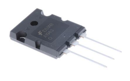
| 描述 | TRANS PNP 250V 17A TO264两极晶体管 - BJT PNP 230V 15A 150W |
| 产品分类 | 晶体管(BJT) - 单路分离式半导体 |
| 品牌 | Fairchild Semiconductor |
| 产品手册 | |
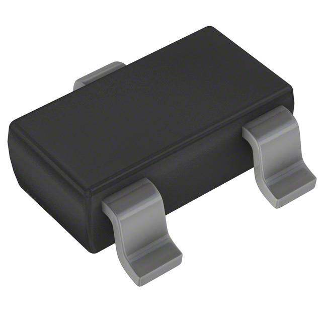
| 产品图片 |
|
| rohs | 符合RoHS无铅 / 符合限制有害物质指令(RoHS)规范要求 |
| 产品系列 | 晶体管,两极晶体管 - BJT,Fairchild Semiconductor 2SA1943OTU- |
| 数据手册 | |
| 产品型号 | 2SA1943OTU |
| PCN封装 | |
| 不同 Ib、Ic时的 Vce饱和值(最大值) | 3V @ 800mA,8A |
| 不同 Ic、Vce 时的DC电流增益(hFE)(最小值) | 80 @ 1A,5V |
| 产品目录页面 | |
| 产品种类 | 两极晶体管 - BJT |
| 供应商器件封装 | TO-264 |
| 功率-最大值 | 150W |
| 包装 | 管件 |
| 单位重量 | 6.756 g |
| 发射极-基极电压VEBO | 5 V |
| 商标 | Fairchild Semiconductor |
| 增益带宽产品fT | 30 MHz |
| 安装类型 | 通孔 |
| 安装风格 | Through Hole |
| 封装 | Tube |
| 封装/外壳 | TO-264-3,TO-264AA |
| 封装/箱体 | TO-264-3 |
| 工厂包装数量 | 25 |
| 晶体管极性 | PNP |
| 晶体管类型 | PNP |
| 最大功率耗散 | 150000 mW |
| 最大工作温度 | + 150 C |
| 最大直流电集电极电流 | 17 A |
| 最小工作温度 | - 50 C |
| 标准包装 | 25 |
| 电压-集射极击穿(最大值) | 250V |
| 电流-集电极(Ic)(最大值) | 17A |
| 电流-集电极截止(最大值) | - |
| 直流集电极/BaseGainhfeMin | 80 at 1 A at 5 V |
| 系列 | 2SA1943 |
| 配置 | Single |
| 集电极—发射极最大电压VCEO | 230 V |
| 集电极—基极电压VCBO | 230 V |
| 集电极连续电流 | 13 A |
| 频率-跃迁 | 30MHz |


- 商务部:美国ITC正式对集成电路等产品启动337调查
- 曝三星4nm工艺存在良率问题 高通将骁龙8 Gen1或转产台积电
- 太阳诱电将投资9.5亿元在常州建新厂生产MLCC 预计2023年完工
- 英特尔发布欧洲新工厂建设计划 深化IDM 2.0 战略
- 台积电先进制程称霸业界 有大客户加持明年业绩稳了
- 达到5530亿美元!SIA预计今年全球半导体销售额将创下新高
- 英特尔拟将自动驾驶子公司Mobileye上市 估值或超500亿美元
- 三星加码芯片和SET,合并消费电子和移动部门,撤换高东真等 CEO
- 三星电子宣布重大人事变动 还合并消费电子和移动部门
- 海关总署:前11个月进口集成电路产品价值2.52万亿元 增长14.8%


PDF Datasheet 数据手册内容提取
Is Now Part of To learn more about ON Semiconductor, please visit our website at www.onsemi.com Please note: As part of the Fairchild Semiconductor integration, some of the Fairchild orderable part numbers will need to change in order to meet ON Semiconductor’s system requirements. Since the ON Semiconductor product management systems do not have the ability to manage part nomenclature that utilizes an underscore (_), the underscore (_) in the Fairchild part numbers will be changed to a dash (-). This document may contain device numbers with an underscore (_). Please check the ON Semiconductor website to verify the updated device numbers. The most current and up-to-date ordering information can be found at www.onsemi.com. Please email any questions regarding the system integration to Fairchild_questions@onsemi.com. ON Semiconductor and the ON Semiconductor logo are trademarks of Semiconductor Components Industries, LLC dba ON Semiconductor or its subsidiaries in the United States and/or other countries. ON Semiconductor owns the rights to a number of patents, trademarks, copyrights, trade secrets, and other intellectual property. A listing of ON Semiconductor’s product/patent coverage may be accessed at www.onsemi.com/site/pdf/Patent-Marking.pdf. ON Semiconductor reserves the right to make changes without further notice to any products herein. ON Semiconductor makes no warranty, representation or guarantee regarding the suitability of its products for any particular purpose, nor does ON Semiconductor assume any liability arising out of the application or use of any product or circuit, and specifically disclaims any and all liability, including without limitation special, consequential or incidental damages. Buyer is responsible for its products and applications using ON Semiconductor products, including compliance with all laws, regulations and safety requirements or standards, regardless of any support or applications information provided by ON Semiconductor. “Typical” parameters which may be provided in ON Semiconductor data sheets and/or specifications can and do vary in different applications and actual performance may vary over time. All operating parameters, including “Typicals” must be validated for each customer application by customer’s technical experts. ON Semiconductor does not convey any license under its patent rights nor the rights of others. ON Semiconductor products are not designed, intended, or authorized for use as a critical component in life support systems or any FDA Class 3 medical devices or medical devices with a same or similar classification in a foreign jurisdiction or any devices intended for implantation in the human body. Should Buyer purchase or use ON Semiconductor products for any such unintended or unauthorized application, Buyer shall indemnify and hold ON Semiconductor and its officers, employees, subsidiaries, affiliates, and distributors harmless against all claims, costs, damages, and expenses, and reasonable attorney fees arising out of, directly or indirectly, any claim of personal injury or death associated with such unintended or unauthorized use, even if such claim alleges that ON Semiconductor was negligent regarding the design or manufacture of the part. ON Semiconductor is an Equal Opportunity/Affirmative Action Employer. This literature is subject to all applicable copyright laws and is not for resale in any manner.
2 S A 1 January 2009 9 4 3 / F 2SA1943/FJL4215 J L 4 PNP Epitaxial Silicon Transistor 2 1 5 — Applications P N • High-Fidelity Audio Output Amplifier P • General Purpose Power Amplifier E p Features i t a • High Current Capability: I = -17A. x C i • High Power Dissipation : 150watts. TO-264 a 1 l • High Frequency : 30MHz. S 1.Base 2.Collector 3.Emitter • High Voltage : VCEO= -250V ili • Wide S.O.A for reliable operation. c o • Excellent Gain Linearity for low THD. n • Complement to 2SC5200/FJL4315. T • Full thermal and electrical Spice models are available. r a • Same transistor is also available in: n -- TO3P package, 2SA1962/FJA4213 : 130 watts s i -- TO220 package, FJP1943 : 80 watts s t -- TO220F package, FJPF1943 : 50 watts o r Absolute Maximum Ratings* Ta = 25°C unless otherwise noted Symbol Parameter Ratings Units BV Collector-Base Voltage -250 V CBO BV Collector-Emitter Voltage -250 V CEO BV Emitter-Base Voltage -5 V EBO I Collector Current -17 A C I Base Current -1.5 A B P Total Device Dissipation(T =25°C) 150 W D C Derate above 25°C 1.04 W/°C T , T Junction and Storage Temperature - 50 ~ +150 °C J STG * These ratings are limiting values above which the serviceability of any semiconductor device may be impaired. Thermal Characteristics* Ta=25°C unless otherwise noted Symbol Parameter Max. Units R Thermal Resistance, Junction to Case 0.83 °C/W θJC * Device mounted on minimum pad size h Classification FE Classification R O h 55 ~ 110 80 ~ 160 FE1 © 2009 Fairchild Semiconductor Corporation www.fairchildsemi.com 2SA1943/FJL4215 Rev. C 1
2 S Electrical Characteristics* A Ta=25°C unless otherwise noted 1 9 Symbol Parameter Test Condition Min. Typ. Max. Units 4 3 / BV Collector-Base Breakdown Voltage I =-5mA, I =0 -250 V F CBO C E J L BVCEO Collector-Emitter Breakdown Voltage IC=-10mA, RBE=∞ -250 V 4 2 BV Emitter-Base Breakdown Voltage I =-5mA, I =0 -5 V 1 EBO E C 5 I Collector Cut-off Current V =-230V, I =0 -5.0 µA — CBO CB E P I Emitter Cut-off Current V =-5V, I =0 -5.0 µA EBO EB C N P h DC Current Gain V =-5V, I =-1A 55 160 FE1 CE C E h DC Current Gain V =-5V, I =-7A 35 60 p FE2 CE C i t a VCE(sat) Collector-Emitter Saturation Voltage IC=-8A, IB=-0.8A -0.4 -3.0 V x i a VBE(on) Base-Emitter On Voltage VCE=-5V, IC=-7A -1.0 -1.5 V l S f Current Gain Bandwidth Product V =-5V, I =-1A 30 MHz i T CE C l i c C Output Capacitance V =-10V, f=1MHz 360 pF o ob CB n * Pulse Test: Pulse Width=20µs, Duty Cycle≤2% T r a n s Ordering Information is t o Part Number Marking Package Packing Method Remarks r 2SA1943RTU A1943R TO-264 TUBE hFE1 R grade 2SA1943OTU A1943O TO-264 TUBE hFE1 O grade FJL4215RTU J4215R TO-264 TUBE hFE1 R grade FJL4215OTU J4215O TO-264 TUBE hFE1 O grade © 2009 Fairchild Semiconductor Corporation www.fairchildsemi.com 2SA1943/FJL4215 Rev. C 2
2 S Typical Characteristics A 1 9 4 3 / F J -20 I = -900mA L I = -1A B CURRENT ---111468 B IIBIB B = == -- 6-54000000mmmAAAIIBB == --870000mmAA GAIN 100 Tj = 125oC Tj = 25oC VCE = -5V 4215 — LECTOR --1102 IIBB == --320000mmAA RRENT Tj = -25oC PNP A], COL --68 IB = -100mA DC CU 10 Ep I[mC -4 h, FE ita x -2 i a 1 l -0 -2 -4 -6 -8 -10 0.1 1 10 S I[A], COLLECTOR CURRENT i VCE[V], COLLECTOR-EMITTER VOLTAGE C lic o Figure 1. Static Characteristic Figure 2. DC current Gain ( R Grade ) n T r a n s 10000 i s Tj = 125oC Tj = 25oC V = -5V GE Ic=-10Ib to CE TA r L N 100 O GAI N V 1000 T Tj = -25oC O N TI E A RR UR U T Tj=25oC C 10 A Tj=125oC h, DC FE at)[mV], S 100 Tj=-25oC s e( 1 Vc 10 0.1 1 10 0.1 1 10 I[A], COLLECTOR CURRENT Ic[A], COLLECTOR CURRENT C Figure 3. DC current Gain ( O Grade ) Figure 4. Collector-Emitter Saturation Voltage 14 10000 E Ic=-10Ib 12 G TA NT VCE = 5V OL RE 10 V R TION Tj=-25oC Tj=25oC OR CU 8 URA 1000 ECT 6 V], SAT Tj=125oC A], COLL 4 at)[m I[C 2 s e( 0 Vb 100 0.0 0.2 0.4 0.6 0.8 1.0 1.2 1.4 1.6 1.8 2.0 2.2 2.4 0.1 1 10 Ic[A], COLLECTOR CURRENT VBE[V], BASE-EMITTER VOLTAGE Figure 5. Base-Emitter Saturation Voltage Figure 6. Base-Emitter On Voltage © 2009 Fairchild Semiconductor Corporation www.fairchildsemi.com 2SA1943/FJL4215 Rev. C 3
2 S Typical Characteristics A 1 9 4 3 / F 100 J C / W] 01..90 T IC MAX. (Pulsed*) L42 oe, R[thjc 00..78 URREN 10 IC MAX. (DC) 100ms*10ms* 15 — anc 0.6 R C DC P Resist 00..45 ECTO 1 NP al LL E m 0.3 O nsient Ther 00..12 I [A], CC0.00.11 * PSUINLGSLEE T NC=O2N5R[oCE]PETITIVE pitaxia a 1E-6 1E-5 1E-4 1E-3 0.01 0.1 1 1 10 100 l Tr S Pulse duration [sec] VCE [V], COLLECTOR-EMITTER VOLTAGE ili c o Figure 7. Thermal Resistance Figure 8. Safe Operating Area n T r a n s 160 i s t 140 o r N O 120 TI A P 100 SI S DI 80 R E W 60 O P W], 40 P[C 20 0 0 25 50 75 100 125 150 175 T[oC], CASE TEMPERATURE C Figure 9. Power Derating © 2009 Fairchild Semiconductor Corporation www.fairchildsemi.com 2SA1943/FJL4215 Rev. C 4
18.30 17.70 B 2109..2800 54..2800 A 16.60 1.00 7.40 2.00 12.00 6.20 3.50 7.00 C R2.00 C 5.80 3.10 0.254 A B 1.20 0.80 9.10 C 0.50 21.62 8.90 21.02 20.20 19.80 R1.00 C 1.70 1.30 1.50 4.05 3.20 2.60 C 2.80 2.40 3.10 1.50 1.50 C 2.70 20.50 2.50 C 2X C 2.30 19.50 1.25 C 0.90 0.254 M A B 5.75 5.75 0.85 C 5.15 5.15 0.50 FRONT VIEW SIDE VIEW BACK VIEW 3.70 5.20 0.15 3.30 4.80 BOTTOM VIEW NOTES: A. PACKAGE REFERENCE: JEDEC TO264 VARIATION AA. B. ALL DIMENSIONS ARE IN MILLIMETERS. C OUT OF JEDEC STANDARD VALUE. D. DIMENSION AND TOLERANCE AS PER ASME Y14.5-1994. E. DIMENSIONS ARE EXCLUSIVE OF BURRS, MOLD FLASH AND TIE BAR PROTRUSIONS. F. THIS PACKAGE IS INTENDED ONLY FOR "FS PKG CODE AR" G. DRAWING FILE NAME: TO264A03REV2
ON Semiconductor and are trademarks of Semiconductor Components Industries, LLC dba ON Semiconductor or its subsidiaries in the United States and/or other countries. ON Semiconductor owns the rights to a number of patents, trademarks, copyrights, trade secrets, and other intellectual property. A listing of ON Semiconductor’s product/patent coverage may be accessed at www.onsemi.com/site/pdf/Patent−Marking.pdf. ON Semiconductor reserves the right to make changes without further notice to any products herein. ON Semiconductor makes no warranty, representation or guarantee regarding the suitability of its products for any particular purpose, nor does ON Semiconductor assume any liability arising out of the application or use of any product or circuit, and specifically disclaims any and all liability, including without limitation special, consequential or incidental damages. Buyer is responsible for its products and applications using ON Semiconductor products, including compliance with all laws, regulations and safety requirements or standards, regardless of any support or applications information provided by ON Semiconductor. “Typical” parameters which may be provided in ON Semiconductor data sheets and/or specifications can and do vary in different applications and actual performance may vary over time. All operating parameters, including “Typicals” must be validated for each customer application by customer’s technical experts. ON Semiconductor does not convey any license under its patent rights nor the rights of others. ON Semiconductor products are not designed, intended, or authorized for use as a critical component in life support systems or any FDA Class 3 medical devices or medical devices with a same or similar classification in a foreign jurisdiction or any devices intended for implantation in the human body. Should Buyer purchase or use ON Semiconductor products for any such unintended or unauthorized application, Buyer shall indemnify and hold ON Semiconductor and its officers, employees, subsidiaries, affiliates, and distributors harmless against all claims, costs, damages, and expenses, and reasonable attorney fees arising out of, directly or indirectly, any claim of personal injury or death associated with such unintended or unauthorized use, even if such claim alleges that ON Semiconductor was negligent regarding the design or manufacture of the part. ON Semiconductor is an Equal Opportunity/Affirmative Action Employer. This literature is subject to all applicable copyright laws and is not for resale in any manner. PUBLICATION ORDERING INFORMATION LITERATURE FULFILLMENT: N. American Technical Support: 800−282−9855 Toll Free ON Semiconductor Website: www.onsemi.com Literature Distribution Center for ON Semiconductor USA/Canada 19521 E. 32nd Pkwy, Aurora, Colorado 80011 USA Europe, Middle East and Africa Technical Support: Order Literature: http://www.onsemi.com/orderlit Phone: 303−675−2175 or 800−344−3860 Toll Free USA/Canada Phone: 421 33 790 2910 Fax: 303−675−2176 or 800−344−3867 Toll Free USA/Canada Japan Customer Focus Center For additional information, please contact your local Email: orderlit@onsemi.com Phone: 81−3−5817−1050 Sales Representative © Semiconductor Components Industries, LLC www.onsemi.com www.onsemi.com 1
Mouser Electronics Authorized Distributor Click to View Pricing, Inventory, Delivery & Lifecycle Information: O N Semiconductor: 2SA1943OTU 2SA1943RTU