ICGOO在线商城 > 分立半导体产品 > 晶体管 - 双极 (BJT) - 单 > PZT4403,115
 Datasheet下载
- 型号: PZT4403,115
- 制造商: NXP Semiconductors
- 库位|库存: xxxx|xxxx
- 要求:
| 数量阶梯 | 香港交货 | 国内含税 |
| +xxxx | $xxxx | ¥xxxx |
查看当月历史价格
查看今年历史价格
PZT4403,115产品简介:
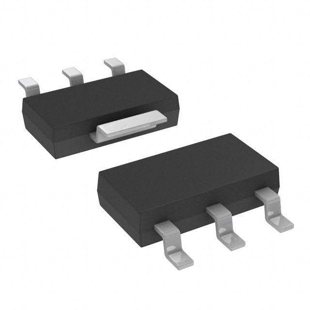
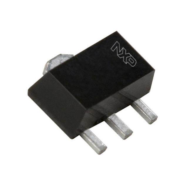
ICGOO电子元器件商城为您提供PZT4403,115由NXP Semiconductors设计生产,在icgoo商城现货销售,并且可以通过原厂、代理商等渠道进行代购。 PZT4403,115价格参考。NXP SemiconductorsPZT4403,115封装/规格:晶体管 - 双极 (BJT) - 单, 双极 (BJT) 晶体管 PNP 40V 600mA 200MHz 1.15W 表面贴装 SOT-223。您可以下载PZT4403,115参考资料、Datasheet数据手册功能说明书,资料中有PZT4403,115 详细功能的应用电路图电压和使用方法及教程。
PZT4403,115 是 Nexperia USA Inc. 生产的一款双极型晶体管(BJT),属于单晶体管类型。该型号的晶体管通常用于以下应用场景:

 1. 开关应用
   - PZT4403,115 可用作电子开关,广泛应用于数字电路中。例如,在继电器驱动、LED 驱动和小型电机控制等场景中,它能够根据输入信号快速切换通断状态。

 2. 信号放大
   - 作为一款 BJT 晶体管,PZT4403,115 能够对微弱的电信号进行电流或电压放大。适用于音频信号放大器、传感器信号调理电路以及无线通信设备中的低噪声放大器。

 3. 电源管理
   - 在直流-直流转换器、线性稳压器或电池管理系统中,该晶体管可以用于调节电流或电压输出,确保负载获得稳定的电源供应。

 4. 保护电路
   - PZT4403,115 可用于过流保护、过压保护或短路保护电路中。通过检测异常电流或电压,晶体管可以切断电路以保护其他元器件。

 5. 脉宽调制 (PWM) 控制
   - 在 PWM 应用中,该晶体管可以用作功率级元件,控制输出信号的占空比。典型应用包括 LED 调光、风扇速度控制和小型加热器的功率调节。

 6. 射频与高频应用
   - 尽管主要为通用晶体管,PZT4403,115 在某些情况下也可用于低频射频电路中,例如振荡器、混频器或调制解调器。

 总结
PZT4403,115 的具体应用场景取决于其电气参数(如集电极-发射极电压、电流增益、最大功耗等)。在实际使用中,需要根据电路设计需求选择合适的偏置条件和外围元件,以充分发挥其性能。
| 参数 | 数值 |
| 产品目录 | |
| 描述 | TRANS PNP SW 40V 600MA SOT-223两极晶体管 - BJT PNP SW 40V 600MA |
| 产品分类 | 晶体管(BJT) - 单路分离式半导体 |
| 品牌 | NXP Semiconductors |
| 产品手册 | |
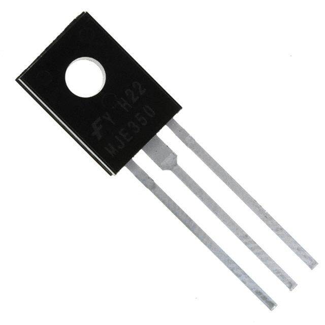
| 产品图片 |
|
| rohs | 符合RoHS无铅 / 符合限制有害物质指令(RoHS)规范要求 |
| 产品系列 | 晶体管,两极晶体管 - BJT,NXP Semiconductors PZT4403,115- |
| 数据手册 | |
| 产品型号 | PZT4403,115 |
| PCN封装 | |
| PCN设计/规格 | |
| 不同 Ib、Ic时的 Vce饱和值(最大值) | 750mV @ 50mA,500mA |
| 不同 Ic、Vce 时的DC电流增益(hFE)(最小值) | 100 @ 150mA,1V |
| 产品目录页面 | |
| 产品种类 | 两极晶体管 - BJT |
| 供应商器件封装 | SC-73 |
| 其它名称 | 568-2457-6 |
| 功率-最大值 | 1.15W |
| 包装 | Digi-Reel® |
| 发射极-基极电压VEBO | 6 V |
| 商标 | NXP Semiconductors |
| 增益带宽产品fT | 200 MHz |
| 安装类型 | 表面贴装 |
| 安装风格 | SMD/SMT |
| 封装 | Reel |
| 封装/外壳 | TO-261-4,TO-261AA |
| 封装/箱体 | SOT-223 |
| 工厂包装数量 | 1000 |
| 晶体管极性 | PNP |
| 晶体管类型 | PNP |
| 最大功率耗散 | 1150 mW |
| 最大工作温度 | + 150 C |
| 最大直流电集电极电流 | 0.6 A |
| 最小工作温度 | - 65 C |
| 标准包装 | 1 |
| 特色产品 | http://www.digikey.com/cn/zh/ph/NXP/I2C.html |
| 电压-集射极击穿(最大值) | 40V |
| 电流-集电极(Ic)(最大值) | 600mA |
| 电流-集电极截止(最大值) | - |
| 直流电流增益hFE最大值 | 30 at 0.1 mA at 1 V |
| 直流集电极/BaseGainhfeMin | 30 at 0.1 mA at 1 V, 60 at 1 mA at 1 V, 100 at 10 mA at 1 V, 100 at 150 mA at 2 V, 20 at 500 mA at 2 V |
| 配置 | Single |
| 集电极—发射极最大电压VCEO | 40 V |
| 集电极—基极电压VCBO | 40 V |
| 零件号别名 | PZT4403 T/R |
| 频率-跃迁 | 200MHz |

SOT223-1.jpg)


- 商务部:美国ITC正式对集成电路等产品启动337调查
- 曝三星4nm工艺存在良率问题 高通将骁龙8 Gen1或转产台积电
- 太阳诱电将投资9.5亿元在常州建新厂生产MLCC 预计2023年完工
- 英特尔发布欧洲新工厂建设计划 深化IDM 2.0 战略
- 台积电先进制程称霸业界 有大客户加持明年业绩稳了
- 达到5530亿美元!SIA预计今年全球半导体销售额将创下新高
- 英特尔拟将自动驾驶子公司Mobileye上市 估值或超500亿美元
- 三星加码芯片和SET,合并消费电子和移动部门,撤换高东真等 CEO
- 三星电子宣布重大人事变动 还合并消费电子和移动部门
- 海关总署:前11个月进口集成电路产品价值2.52万亿元 增长14.8%


PDF Datasheet 数据手册内容提取
PZT4403 40 V, 600 mA PNP switching transistor Rev. 03 — 2 March 2010 Product data sheet 1. Product profile 1.1 General description PNP switching transistor in a medium power SOT223(SC-73) small Surface-Mounted Device(SMD) plastic package. NPN complement: PZT4401. 1.2 Features and benefits (cid:132) High current (max.600mA) (cid:132) Low voltage (max.40V) 1.3 Applications (cid:132) Switching and linear amplification 1.4 Quick reference data Table 1. Quick reference data Symbol Parameter Conditions Min Max Unit V collector-emitter voltage open base - - −40 V CEO I collector current - - −600 mA C h DCcurrent gain V =−1V; [1] 100 - 300 FE CE I =−150mA C [1] Pulse test: tp≤300μs;δ≤0.02. 2. Pinning information Table 2. Pinning Pin Description Simplified outline Graphic symbol 1 base 4 2, 4 2,4 collector 3 emitter 1 1 2 3 3 sym028
PZT4403 Nexperia 40 V, 600 mA PNP switching transistor 3. Ordering information Table 3. Ordering information Type number Package Name Description Version PZT4403 SC-73 plastic surface-mounted package with increased SOT223 heatsink; 4 leads 4. Marking Table 4. Marking codes Type number Marking code PZT4403 ZT4403 5. Limiting values Table 5. Limiting values In accordance with the Absolute Maximum Rating System (IEC 60134). Symbol Parameter Conditions Min Max Unit V collector-base voltage open emitter - −40 V CBO V collector-emitter voltage open base - −40 V CEO V emitter-base voltage open collector - −6 V EBO I collector current - −600 mA C I peak collector current - −800 mA CM I peak base current - −200 mA BM P total power dissipation T ≤25°C [1] - 1150 mW tot amb T junction temperature - 150 °C j T ambient temperature −65 +150 °C amb T storage temperature −65 +150 °C stg [1] Device mounted on anFR4Printed-Circuit Board(PCB), single-sided copper, tin-plated, mounting pad for collector 1cm2. 6. Thermal characteristics Table 6. Thermal characteristics Symbol Parameter Conditions Min Typ Max Unit R thermal resistance from in free air [1] - - 106 K/W th(j-a) junction to ambient R thermal resistance from - - 25 K/W th(j-sp) junction to solder point [1] Device mounted on an FR4PCB, single-sided copper, tin-plated, mounting pad for collector 1cm2. PZT4403_3 All information provided in this document is subject to legal disclaimers. © Nexperia B.V. 2017. All rights reserved Product data sheet Rev. 03 — 2 March 2010 2 of 9
PZT4403 Nexperia 40 V, 600 mA PNP switching transistor 7. Characteristics Table 7. Characteristics T =25°C unless otherwise specified. amb Symbol Parameter Conditions Min Typ Max Unit I collector-base V =−40V; I =0A - - −50 nA CBO CB E cut-offcurrent I emitter-base V =−5V; I =0A - - −50 nA EBO EB C cut-offcurrent h DCcurrent gain V =−1V; 30 - - FE CE I =−0.1mA C V =−1V; 60 - - CE I =−1mA C V =−1V; 100 - - CE I =−10mA C V =−1V; [1] 100 - 300 CE I =−150mA C V =−2V; [1] 20 - - CE I =−500mA C V collector-emitter I =−150mA; [1] - - −400 mV CEsat C saturation voltage I =−15mA B I =−500mA; [1] - - −750 mV C I =−50mA B V base-emitter I =−150mA; [1] - - −950 mV BEsat C saturationvoltage I =−15mA B I =−500mA; [1] - - −1300 mV C I =−50mA B t delay time V =−29.5V; - - 15 ns d CC I =−150mA; t rise time C - - 30 ns r I =−15mA; Bon ton turn-on time IBoff=15mA; - - 40 ns ts storage time VBB=3.5V - - 300 ns t fall time - - 50 ns f t turn-off time - - 350 ns off f transition frequency V =−10V; 200 - - MHz T CE I =−20mA; C f=100MHz C collector capacitance V =−5V; - - 8.5 pF c CB I =i =0A; E e f=1MHz C emitter capacitance V =−500mV; - - 35 pF e EB I =i =0A; C c f=1MHz [1] Pulse test: tp≤300μs;δ≤0.02. PZT4403_3 All information provided in this document is subject to legal disclaimers. © Nexperia B.V. 2017. All rights reserved Product data sheet Rev. 03 — 2 March 2010 3 of 9
PZT4403 Nexperia 40 V, 600 mA PNP switching transistor mgs333 300 hFE 200 100 0 −10−1 −1 −10 −102 −103 IC (mA) VCE=−1V Fig 1. DCcurrent gain as a function of collector current; typical values 8. Test information VBB VCC RB RC (probe) Vo (probe) oscilloscope oscilloscope 450 Ω 450 Ω R2 VI DUT R1 mgd624 Vi=−9.5V; T=500μs; tp=10μs R1=68Ω; R2=325Ω;RB=325Ω; RC=160Ω VBB=3.5V; VCC=−29.5V Oscilloscope input impedance Zi=50Ω Fig 2. Test circuit for switching times PZT4403_3 All information provided in this document is subject to legal disclaimers. © Nexperia B.V. 2017. All rights reserved Product data sheet Rev. 03 — 2 March 2010 4 of 9
PZT4403 Nexperia 40 V, 600 mA PNP switching transistor 9. Package outline 6.7 6.3 1.8 3.1 1.5 2.9 4 1.1 0.7 7.3 3.7 6.7 3.3 1 2 3 0.8 0.32 2.3 0.6 0.22 4.6 Dimensions in mm 04-11-10 Fig 3. Package outline SOT223(SC-73) 10. Packing information Table 8. Packing methods The indicated -xxx are the last three digits of the 12NC ordering code.[1] Type number Package Description Packing quantity 1000 4000 PZT4403 SOT223 8mm pitch, 12mm tape and reel -115 -135 [1] For further information and the availability of packing methods, see Section13. PZT4403_3 All information provided in this document is subject to legal disclaimers. © Nexperia B.V. 2017. All rights reserved Product data sheet Rev. 03 — 2 March 2010 5 of 9
PZT4403 Nexperia 40 V, 600 mA PNP switching transistor 11. Revision history Table 9. Revision history Document ID Release date Data sheet status Change notice Supersedes PZT4403_3 20100302 Product data sheet - PZT4403_N_2 Modifications: • The format of this data sheet has been redesigned to comply with the new identity guidelines of NXP Semiconductors. • Legal texts have been adapted to the new company name where appropriate. • Section 1.1 “General description”: amended • Section 1.4 “Quick reference data”: added • Section 3 “Ordering information”: added • Section 4 “Marking”: added • Section 7 “Characteristics”: amended • Section 8 “Test information”: added • Figure3: superseded by minimized package outline drawing • Section 10 “Packing information”: added • Section 12 “Legal information”: updated PZT4403_N_2 20080117 Product data sheet - PZT4403_1 PZT4403_1 19990510 Product specification - - PZT4403_3 All information provided in this document is subject to legal disclaimers. © Nexperia B.V. 2017. All rights reserved Product data sheet Rev. 03 — 2 March 2010 6 of 9
PZT4403 Nexperia 40 V, 600 mA PNP switching transistor 12. Legal information 12.1 Data sheet status Document status[1][2] Product status[3] Definition Objective [short] data sheet Development This document contains data from the objective specification for product development. Preliminary [short] data sheet Qualification This document contains data from the preliminary specification. Product [short] data sheet Production This document contains the product specification. [1] Please consult the most recently issued document before initiating or completing a design. [2] The term ‘short data sheet’ is explained in section “Definitions”. [3] The product status of device(s) described in this document may have changed since this document was published and may differ in case of multiple devices. The latest product status information is available on the Internet at URLhttp://www.nexperia.com. 12.2 Definitions malfunction of a Nexperia product can reasonably be expected to result in personal injury, death or severe property or environmental damage. Nexperia accepts no liability for inclusion and/or use of Draft — The document is a draft version only. The content is still under Nexperia products in such equipment or applications and internal review and subject to formal approval, which may result in therefore such inclusion and/or use is at the customer’s own risk. modifications or additions. Nexperia does not give any representations or warranties as to the accuracy or completeness of Applications — Applications that are described herein for any of these information included herein and shall have no liability for the consequences of products are for illustrative purposes only. Nexperia makes no use of such information. representation or warranty that such applications will be suitable for the specified use without further testing or modification. Short data sheet — A short data sheet is an extract from a full data sheet with the same product type number(s) and title. A short data sheet is intended Nexperia does not accept any liability related to any default, for quick reference only and should not be relied upon to contain detailed and damage, costs or problem which is based on a weakness or default in the full information. For detailed and full information see the relevant full data customer application/use or the application/use of customer’s third party sheet, which is available on request via the local Nexperia sales customer(s) (hereinafter both referred to as “Application”). It is customer’s office. In case of any inconsistency or conflict with the short data sheet, the sole responsibility to check whether the Nexperia product is full data sheet shall prevail. suitable and fit for the Application planned. Customer has to do all necessary testing for the Application in order to avoid a default of the Application and the Product specification — The information and data provided in a Product product. Nexperia does not accept any liability in this respect. data sheet shall define the specification of the product as agreed between Nexperia and its customer, unless Nexperia and Limiting values — Stress above one or more limiting values (as defined in customer have explicitly agreed otherwise in writing. In no event however, the Absolute Maximum Ratings System of IEC60134) will cause permanent shall an agreement be valid in which the Nexperia product is damage to the device. Limiting values are stress ratings only and (proper) deemed to offer functions and qualities beyond those described in the operation of the device at these or any other conditions above those given in Product data sheet. the Recommended operating conditions section (if present) or the Characteristics sections of this document is not warranted. Constant or repeated exposure to limiting values will permanently and irreversibly affect 12.3 Disclaimers the quality and reliability of the device. Terms and conditions of commercial sale — Nexperia Limited warranty and liability — Information in this document is believed to products are sold subject to the general terms and conditions of commercial be accurate and reliable. However, Nexperia does not give any sale, as published at http://www.nexperia.com/profile/terms, unless otherwise representations or warranties, expressed or implied, as to the accuracy or agreed in a valid written individual agreement. In case an individual completeness of such information and shall have no liability for the agreement is concluded only the terms and conditions of the respective consequences of use of such information. agreement shall apply. Nexperia hereby expressly objects to In no event shall Nexperia be liable for any indirect, incidental, applying the customer’s general terms and conditions with regard to the punitive, special or consequential damages (including - without limitation - lost purchase of Nexperia products by customer. profits, lost savings, business interruption, costs related to the removal or No offer to sell or license — Nothing in this document may be interpreted or replacement of any products or rework charges) whether or not such construed as an offer to sell products that is open for acceptance or the grant, damages are based on tort (including negligence), warranty, breach of conveyance or implication of any license under any copyrights, patents or contract or any other legal theory. other industrial or intellectual property rights. Notwithstanding any damages that customer might incur for any reason Export control — This document as well as the item(s) described herein whatsoever, Nexperia’s aggregate and cumulative liability towards may be subject to export control regulations. Export might require a prior customer for the products described herein shall be limited in accordance authorization from national authorities. with the Terms and conditions of commercial sale of Nexperia. Quick reference data — The Quick reference data is an extract of the Right to make changes — Nexperia reserves the right to make product data given in the Limiting values and Characteristics sections of this changes to information published in this document, including without document, and as such is not complete, exhaustive or legally binding. limitation specifications and product descriptions, at any time and without notice. This document supersedes and replaces all information supplied prior to the publication hereof. 12.4 Trademarks Suitability for use — Nexperia products are not designed, Notice: All referenced brands, product names, service names and trademarks authorized or warranted to be suitable for use in medical, military, aircraft, are the property of their respective owners. space or life support equipment, nor in applications where failure or PZT4403_3 All information provided in this document is subject to legal disclaimers. © Nexperia B.V. 2017. All rights reserved Product data sheet Rev. 03 — 2 March 2010 7 of 9
PZT4403 Nexperia 40 V, 600 mA PNP switching transistor 13. Contact information For more information, please visit: http://www.nexperia.com For sales office addresses, please send an email to: salesaddresses@nexperia.com PZT4403_3 All information provided in this document is subject to legal disclaimers. © Nexperia B.V. 2017. All rights reserved Product data sheet Rev. 03 — 2 March 2010 8 of 9
PZT4403 Nexperia 40 V, 600 mA PNP switching transistor 14. Contents 1 Product profile. . . . . . . . . . . . . . . . . . . . . . . . . . 1 1.1 General description . . . . . . . . . . . . . . . . . . . . . 1 1.2 Features and benefits. . . . . . . . . . . . . . . . . . . . 1 1.3 Applications . . . . . . . . . . . . . . . . . . . . . . . . . . . 1 1.4 Quick reference data . . . . . . . . . . . . . . . . . . . . 1 2 Pinning information. . . . . . . . . . . . . . . . . . . . . . 1 3 Ordering information. . . . . . . . . . . . . . . . . . . . . 2 4 Marking. . . . . . . . . . . . . . . . . . . . . . . . . . . . . . . . 2 5 Limiting values. . . . . . . . . . . . . . . . . . . . . . . . . . 2 6 Thermal characteristics . . . . . . . . . . . . . . . . . . 2 7 Characteristics. . . . . . . . . . . . . . . . . . . . . . . . . . 3 8 Test information. . . . . . . . . . . . . . . . . . . . . . . . . 4 9 Package outline. . . . . . . . . . . . . . . . . . . . . . . . . 5 10 Packing information . . . . . . . . . . . . . . . . . . . . . 5 11 Revision history. . . . . . . . . . . . . . . . . . . . . . . . . 6 12 Legal information. . . . . . . . . . . . . . . . . . . . . . . . 7 12.1 Data sheet status . . . . . . . . . . . . . . . . . . . . . . . 7 12.2 Definitions. . . . . . . . . . . . . . . . . . . . . . . . . . . . . 7 12.3 Disclaimers. . . . . . . . . . . . . . . . . . . . . . . . . . . . 7 12.4 Trademarks. . . . . . . . . . . . . . . . . . . . . . . . . . . . 7 13 Contact information. . . . . . . . . . . . . . . . . . . . . . 8 14 Contents. . . . . . . . . . . . . . . . . . . . . . . . . . . . . . . 9 © Nexperia B.V. 2017. All rights reserved For more information, please visit: http://www.nexperia.com For sales office addresses, please send an email to: salesaddresses@nexperia.com Date of release: 02 March 2010