ICGOO在线商城 > 分立半导体产品 > 晶体管 - 双极 (BJT) - 单 > PBSS5350X,135
 Datasheet下载
- 型号: PBSS5350X,135
- 制造商: NXP Semiconductors
- 库位|库存: xxxx|xxxx
- 要求:
| 数量阶梯 | 香港交货 | 国内含税 |
| +xxxx | $xxxx | ¥xxxx |
查看当月历史价格
查看今年历史价格
PBSS5350X,135产品简介:
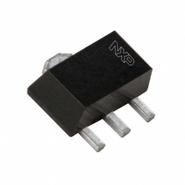
ICGOO电子元器件商城为您提供PBSS5350X,135由NXP Semiconductors设计生产,在icgoo商城现货销售,并且可以通过原厂、代理商等渠道进行代购。 PBSS5350X,135价格参考¥0.51-¥0.51。NXP SemiconductorsPBSS5350X,135封装/规格:晶体管 - 双极 (BJT) - 单, Bipolar (BJT) Transistor PNP 50V 3A 100MHz 1.6W Surface Mount SOT-89。您可以下载PBSS5350X,135参考资料、Datasheet数据手册功能说明书,资料中有PBSS5350X,135 详细功能的应用电路图电压和使用方法及教程。
PBSS5350X,135 是由 Nexperia USA Inc. 生产的一款 NPN 型双极结型晶体管(BJT),属于高性能中功率晶体管系列。该器件采用 SOT457 封装,具有低饱和电压、高电流增益和优良的开关性能,适用于多种中等功率和高效率的应用场景。

典型应用包括:
1. 电源管理电路:用于DC-DC转换器、负载开关和电压调节模块中,实现高效电能转换与控制;
2. LED驱动电路:在中高亮度LED照明系统中作为开关或恒流源驱动元件,提供稳定电流输出;
3. 电机驱动与继电器控制:适用于小型直流电机或电磁继电器的开关控制,具备良好的耐压与电流驱动能力;
4. 消费类电子产品:广泛应用于手机、平板、智能家居设备中的信号切换与功率控制模块;
5. 工业与汽车电子:因其工作温度范围宽(-55°C 至 +150°C)、可靠性高,适合汽车电子控制单元(ECU)、传感器驱动和车载电源系统。

PBSS5350X,135 具有最高 50V 的集射极击穿电压(VCEO)和最大 500mA 的连续集电极电流(IC),同时具备较低的导通损耗,有助于提升系统能效。其小尺寸封装也利于高密度PCB布局,是兼顾性能与空间效率的理想选择。
| 参数 | 数值 |
| 产品目录 | |
| 描述 | TRANS PNP 50V 3A SOT89两极晶体管 - BJT TRANS BISS TAPE-11 |
| 产品分类 | 晶体管(BJT) - 单路分离式半导体 |
| 品牌 | NXP Semiconductors |
| 产品手册 | |
| 产品图片 |
|
| rohs | 符合RoHS无铅 / 符合限制有害物质指令(RoHS)规范要求 |
| 产品系列 | 晶体管,两极晶体管 - BJT,NXP Semiconductors PBSS5350X,135- |
| 数据手册 | |
| 产品型号 | PBSS5350X,135 |
| PCN封装 | |
| PCN组件/产地 | |
| PCN设计/规格 | |
| 不同 Ib、Ic时的 Vce饱和值(最大值) | 390mV @ 300mA,3A |
| 不同 Ic、Vce 时的DC电流增益(hFE)(最小值) | 200 @ 1A,2V |
| 产品种类 | Transistors - Arrays |
| 供应商器件封装 | SOT-89-3 |
| 其它名称 | 568-6779-2 |
| 功率-最大值 | 1.6W |
| 包装 | 带卷 (TR) |
| 发射极-基极电压VEBO | - 5 V |
| 商标 | NXP Semiconductors |
| 增益带宽产品fT | 100 MHz |
| 安装类型 | 表面贴装 |
| 安装风格 | SMD/SMT |
| 封装 | Reel |
| 封装/外壳 | TO-243AA |
| 封装/箱体 | TO-243 |
| 工厂包装数量 | 4000 |
| 晶体管极性 | PNP |
| 晶体管类型 | PNP |
| 最大功率耗散 | 550 mW |
| 最大工作温度 | + 150 C |
| 最大直流电集电极电流 | - 5 A |
| 最小工作温度 | - 65 C |
| 标准包装 | 4,000 |
| 特色产品 | http://www.digikey.com/cn/zh/ph/NXP/I2C.html |
| 电压-集射极击穿(最大值) | 50V |
| 电流-集电极(Ic)(最大值) | 3A |
| 电流-集电极截止(最大值) | 100nA |
| 直流电流增益hFE最大值 | 200 at 0.1 A at 2 V |
| 直流集电极/BaseGainhfeMin | 200 |
| 配置 | Single |
| 集电极—发射极最大电压VCEO | - 50 V |
| 集电极—基极电压VCBO | 50 V |
| 集电极连续电流 | - 3 A |
| 零件号别名 | /T3 PBSS5350X |
| 频率-跃迁 | 100MHz |

SOT89.jpg)


- 商务部:美国ITC正式对集成电路等产品启动337调查
- 曝三星4nm工艺存在良率问题 高通将骁龙8 Gen1或转产台积电
- 太阳诱电将投资9.5亿元在常州建新厂生产MLCC 预计2023年完工
- 英特尔发布欧洲新工厂建设计划 深化IDM 2.0 战略
- 台积电先进制程称霸业界 有大客户加持明年业绩稳了
- 达到5530亿美元!SIA预计今年全球半导体销售额将创下新高
- 英特尔拟将自动驾驶子公司Mobileye上市 估值或超500亿美元
- 三星加码芯片和SET,合并消费电子和移动部门,撤换高东真等 CEO
- 三星电子宣布重大人事变动 还合并消费电子和移动部门
- 海关总署:前11个月进口集成电路产品价值2.52万亿元 增长14.8%


PDF Datasheet 数据手册内容提取
Important notice Dear Customer, On 7 February 2017 the former NXP Standard Product business became a new company with the tradename Nexperia. Nexperia is an industry leading supplier of Discrete, Logic and PowerMOS semiconductors with its focus on the automotive, industrial, computing, consumer and wearable application markets In data sheets and application notes which still contain NXP or Philips Semiconductors references, use the references to Nexperia, as shown below. Instead of http://www.nxp.com, http://www.philips.com/ or http://www.semiconductors.philips.com/, use http://www.nexperia.com Instead of sales.addresses@www.nxp.com or sales.addresses@www.semiconductors.philips.com, use salesaddresses@nexperia.com (email) Replace the copyright notice at the bottom of each page or elsewhere in the document, depending on the version, as shown below: - © NXP N.V. (year). All rights reserved or © Koninklijke Philips Electronics N.V. (year). All rights reserved Should be replaced with: - © Nexperia B.V. (year). All rights reserved. If you have any questions related to the data sheet, please contact our nearest sales office via e-mail or telephone (details via salesaddresses@nexperia.com). Thank you for your cooperation and understanding, Kind regards, Team Nexperia
DISCRETE SEMICONDUCTORS DATA SHEET dbook, halfpage M3D109 PBSS5350X 50 V, 3 A PNP low V (BISS) transistor CEsat Product data sheet 2004 Nov 04 Supersedes data of 2003 Nov 21
NXP Semiconductors Product data sheet 50 V, 3 A PBSS5350X PNP low V (BISS) transistor CEsat FEATURES QUICK REFERENCE DATA • SOT89 (SC-62) package SYMBOL PARAMETER MAX. UNIT • Low collector-emitter saturation voltage V CEsat V collector-emitter voltage −50 V CEO • High collector current capability: IC and ICM IC collector current (DC) −3 A • Higher efficiency leading to less heat generation I peak collector current −5 A CM • Reduced printed-circuit board requirements. R equivalent on-resistance 135 mΩ CEsat APPLICATIONS PINNING • Power management PIN DESCRIPTION – DC/DC converters 1 emitter – Supply line switching 2 collector – Battery charger 3 base – LCD backlighting. • Peripheral drivers – Driver in low supply voltage applications (e.g. lamps and LEDs). – Inductive load driver (e.g. relays, buzzers and motors). 2 3 DESCRIPTION PNP low V transistor in a SOT89 plastic package. 1 CEsat NPN complement: PBSS4350X. sym079 3 2 1 MARKING TYPE NUMBER MARKING CODE Fig.1 Simplified outline (SOT89) and symbol. PBSS5350X S46 2004 Nov 04 2
NXP Semiconductors Product data sheet 50 V, 3 A PBSS5350X PNP low V (BISS) transistor CEsat ORDERING INFORMATION PACKAGE TYPE NUMBER NAME DESCRIPTION VERSION PBSS5350X SC-62 plastic surface mounted package; collector pad for good heat SOT89 transfer; 3 leads LIMITING VALUES In accordance with the Absolute Maximum Rating System (IEC 60134). SYMBOL PARAMETER CONDITIONS MIN. MAX. UNIT V collector-base voltage open emitter − −50 V CBO V collector-emitter voltage open base − −50 V CEO V emitter-base voltage open collector − −5 V EBO I collector current (DC) note 4 − −3 A C I peak collector current limited by T − −5 A CM j(max) I base current (DC) − −0.5 A B P total power dissipation T ≤ 25 °C tot amb note 1 − 550 mW note 2 − 1 W note 3 − 1.4 W note 4 − 1.6 W T storage temperature −65 +150 °C stg T junction temperature − 150 °C j T ambient temperature −65 +150 °C amb Notes 1. Device mounted on a FR4 printed-circuit board; single-sided copper; tin-plated; standard footprint. 2. Device mounted on a FR4 printed-circuit board; single-sided copper; tin-plated; mounting pad for collector 1 cm2. 3. Device mounted on a FR4 printed-circuit board; single-sided copper; tin-plated; mounting pad for collector 6 cm2. 4. Device mounted on a ceramic printed-circuit board 7 cm2, single-sided copper, tin-plated. 2004 Nov 04 3
NXP Semiconductors Product data sheet 50 V, 3 A PBSS5350X PNP low V (BISS) transistor CEsat MLE186 2 handbook, halfpage Ptot (W) (1) 1.6 (2) 1.2 (3) 0.8 (4) 0.4 0 0 40 80 120 160 Tamb (°C) (1) Ceramic PCB; 7 cm2 (3) FR4 PCB; 1 cm2 copper mounting pad for collector. mounting pad for collector. (2) FR4 PCB; 6 cm2 copper (4) Standard footprint. mounting pad for collector. Fig.2 Power derating curves. 2004 Nov 04 4
NXP Semiconductors Product data sheet 50 V, 3 A PBSS5350X PNP low V (BISS) transistor CEsat THERMAL CHARACTERISTICS SYMBOL PARAMETER CONDITIONS VALUE UNIT R thermal resistance from junction to ambient in free air th(j-a) note 1 225 K/W note 2 125 K/W note 3 90 K/W note 4 80 K/W R thermal resistance from junction to soldering point 16 K/W th(j-s) Notes 1. Device mounted on a FR4 printed-circuit board; single-sided copper; tin-plated; standard footprint. 2. Device mounted on a FR4 printed-circuit board; single-sided copper; tin-plated; mounting pad for collector 1 cm2. 3. Device mounted on a FR4 printed-circuit board; single-sided copper; tin-plated; mounting pad for collector 6 cm2. 4. Device mounted on a ceramic printed-circuit board 7 cm2, single-sided copper, tin-plated. 103 006aaa243 Zth(j-a) duty cycle = (K/W) 1.00 0.75 102 0.50 0.33 0.20 0.10 0.05 10 0.02 0.01 1 0 10−1 10−5 10−4 10−3 10−2 10−1 1 10 102 103 tp (s) Mounted on FR4 printed-circuit board; standard footprint. Fig.3 Transient thermal impedance as a function of pulse time; typical values. 2004 Nov 04 5
NXP Semiconductors Product data sheet 50 V, 3 A PBSS5350X PNP low V (BISS) transistor CEsat 103 006aaa244 Zth(j-a) (K/W) duty cycle = 1.00 102 0.75 0.50 0.33 0.20 0.10 10 0.05 0.02 0.01 1 0 10−1 10−5 10−4 10−3 10−2 10−1 1 10 102 103 tp (s) Mounted on FR4 printed-circuit board; mounting pad for collector 1 cm2. Fig.4 Transient thermal impedance as a function of pulse time; typical values. 103 006aaa245 Zth(j-a) (K/W) duty cycle = 102 1.00 0.75 0.50 0.33 0.20 10 0.10 0.05 0.02 0.01 1 0 10−1 10−5 10−4 10−3 10−2 10−1 1 10 102 103 tp (s) Mounted on FR4 printed-circuit board; mounting pad for collector 6 cm2. Fig.5 Transient thermal impedance as a function of pulse time; typical values. 2004 Nov 04 6
NXP Semiconductors Product data sheet 50 V, 3 A PBSS5350X PNP low V (BISS) transistor CEsat CHARACTERISTICS T = 25 °C unless otherwise specified. amb SYMBOL PARAMETER CONDITIONS MIN. TYP. MAX. UNIT I collector-base cut-off current V = −50 V; I = 0 A − − −100 nA CBO CB E V = −50 V; I = 0 A; T = 150 °C − − −50 μA CB E j I collector-emitter cut-off current V = −50 V; V = 0 V − − −100 nA CES CE BE I emitter-base cut-off current V = −5 V; I = 0 A − − −100 nA EBO EB C h DC current gain V = −2 V FE CE I = −0.1 A 200 − − C I = −0.5 A 200 − − C I = −1 A; note 1 200 − 450 C I = −2 A; note 1 130 − − C I = −3 A; note 1 80 − − C V collector-emitter saturation I = −0.5 A; I = −50 mA − − −90 mV CEsat C B voltage I = −1 A; I = −50 mA − − −180 mV C B I = −2 A; I = −100 mA − − −320 mV C B I = −2 A; I = −200 mA; note 1 − − −270 mV C B I = −3 A; I = −300 mA; note 1 − − −390 mV C B R equivalent on-resistance I = −2 A; I = −200 mA; note 1 − 90 135 mΩ CEsat C B V base-emitter saturation voltage I = −2 A; I = −100 mA − − −1.1 V BEsat C B I = −3 A; I = −300 mA; note 1 − − −1.2 V C B V base-emitter turn-on voltage V = −2 V; I = −1 A −1.1 − − V BEon CE C f transition frequency I = −100 mA; V = −5 V; 100 − − MHz T C CE f = 100 MHz C collector capacitance V = −10 V; I = i = 0 A; f = 1 MHz − − 35 pF c CB E e Note 1. Pulse test: t ≤ 300 μs; δ ≤ 0.02. p 2004 Nov 04 7
NXP Semiconductors Product data sheet 50 V, 3 A PBSS5350X PNP low V (BISS) transistor CEsat 600 MLE171 −1.2 MLE170 handbook, halfpage handbook, halfpage (1) hFE VBE (V) (1) 400 (2) −0.8 (2) (3) 200 (3) −0.4 0 0 −10−1 −1 −10 −102 −103 −104 −10−1 −1 −10 −102 −103 −104 IC (mA) IC (mA) VCE = −2 V. VCE = −2 V. (1) Tamb = 100 °C. (1) Tamb = −55 °C. (2) Tamb = 25 °C. (2) Tamb = 25 °C. (3) Tamb = −55 °C. (3) Tamb = 100 °C. Fig.6 DC current gain as a function of collector Fig.7 Base-emitter voltage as a function of current; typical values. collector current; typical values. MLE173 MLE174 −1 −1 handbook, halfpage handbook, halfpage VCEsat VCEsat (V) (V) −10−1 −10−1 (1) (2) (2) (1) −10−2 (3) −10−2 (3) −10−3 −10−3 −10−1 −1 −10 −102 −103 −104 −10−1 −1 −10 −102 −103 −104 IC (mA) IC (mA) IC/IB = 20. Tamb = 25 °C. (1) Tamb = 100 °C. (1) IC/IB = 100. (2) Tamb = 25 °C. (2) IC/IB = 50. (3) Tamb = −55 °C. (3) IC/IB = 10. Fig.8 Collector-emitter saturation voltage as a Fig.9 Collector-emitter saturation voltage as a function of collector current; typical values. function of collector current; typical values. 2004 Nov 04 8
NXP Semiconductors Product data sheet 50 V, 3 A PBSS5350X PNP low V (BISS) transistor CEsat −1.2 MLE175 103 MLE172 handVbBooEks, ahtalfpage handRbCooEks, haatlfpage (Ω) (V) −1 102 (1) −0.8 (2) 10 (3) −0.6 1 (1) (2) −0.4 10−1 (3) −0.−210−1 −1 −10 −102 −103 −104 10−−210−1 −1 −10 −102 −103 −104 IC (mA) IC (mA) IC/IB = 20. IC/IB = 20. (1) Tamb = −55 °C. (2) Tamb = 25 °C. (3) Tamb = 100 °C. (1) Tamb = 150 °C. (2) Tamb = 25 °C. (3) Tamb = −55 °C. Fig.10 Base-emitter saturation voltage as a Fig.11 Equivalent on-resistance as a function of function of collector current; typical values. collector current; typical values. MLE168 MLE169 −1 −5 handbookIC, halfpage (1) handbookIC, halfpage (7) (6) (5) (4) (3) (2) (1) (A) (2) (A) −0.8 (3) −4 (4) (5) −0.6 −3 (8) (6) (9) (7) −0.4 (8) −2 (10) (9) −0.2 −1 (10) 0 0 0 −0.4 −0.8 −1.2 −1.6 −2 0 −0.4 −0.8 −1.2 −1.6 −2 VCE (V) VCE (V) Tamb = 25 °C. Tamb = 25 °C. (1) IB = −3500 μA. (5) IB = −2100 μA. (9) IB = −700 μA. (1) IB = −140 mA. (5) IB = −84 mA. (9) IB = −28 mA. (2) IB = −3150 μA. (6) IB = −1750 μA. (10)IB = −350 μA. (2) IB = −126 mA. (6) IB = −70 mA. (10)IB = −14 mA. (3) IB = −2800 μA. (7) IB = −1400 μA. (3) IB = −112 mA. (7) IB = −56 mA. (4) IB = −2450 μA. (8) IB = −1050 μA. (4) IB = −98 mA. (8) IB = −42 mA. Fig.12 Collector current as a function of Fig.13 Collector current as a function of collector-emitter voltage; typical values. collector-emitter voltage; typical values. 2004 Nov 04 9
NXP Semiconductors Product data sheet 50 V, 3 A PBSS5350X PNP low V (BISS) transistor CEsat PACKAGE OUTLINE Plastic surface-mounted package; collector pad for good heat transfer; 3 leads SOT89 D B A bp3 E HE Lp 1 2 3 bp2 c w M bp1 e1 e 0 2 4 mm scale DIMENSIONS (mm are the original dimensions) UNIT A bp1 bp2 bp3 c D E e e1 HE Lp w 1.6 0.48 0.53 1.8 0.44 4.6 2.6 4.25 1.2 mm 3.0 1.5 0.13 1.4 0.35 0.40 1.4 0.23 4.4 2.4 3.75 0.8 OUTLINE REFERENCES EUROPEAN ISSUE DATE VERSION IEC JEDEC JEITA PROJECTION 04-08-03 SOT89 TO-243 SC-62 06-03-16 2004 Nov 04 10
NXP Semiconductors Product data sheet 50 V, 3 A PBSS5350X PNP low V (BISS) transistor CEsat DATA SHEET STATUS DOCUMENT PRODUCT DEFINITION STATUS(1) STATUS(2) Objective data sheet Development This document contains data from the objective specification for product development. Preliminary data sheet Qualification This document contains data from the preliminary specification. Product data sheet Production This document contains the product specification. Notes 1. Please consult the most recently issued document before initiating or completing a design. 2. The product status of device(s) described in this document may have changed since this document was published and may differ in case of multiple devices. The latest product status information is available on the Internet at URL http://www.nxp.com. DISCLAIMERS above those given in the Characteristics sections of this document is not implied. Exposure to limiting values for General ⎯ Information in this document is believed to be extended periods may affect device reliability. accurate and reliable. However, NXP Semiconductors does not give any representations or warranties, Terms and conditions of sale ⎯ NXP Semiconductors expressed or implied, as to the accuracy or completeness products are sold subject to the general terms and of such information and shall have no liability for the conditions of commercial sale, as published at consequences of use of such information. http://www.nxp.com/profile/terms, including those pertaining to warranty, intellectual property rights Right to make changes ⎯ NXP Semiconductors infringement and limitation of liability, unless explicitly reserves the right to make changes to information otherwise agreed to in writing by NXP Semiconductors. In published in this document, including without limitation case of any inconsistency or conflict between information specifications and product descriptions, at any time and in this document and such terms and conditions, the latter without notice. This document supersedes and replaces all will prevail. information supplied prior to the publication hereof. No offer to sell or license ⎯ Nothing in this document Suitability for use ⎯ NXP Semiconductors products are may be interpreted or construed as an offer to sell products not designed, authorized or warranted to be suitable for that is open for acceptance or the grant, conveyance or use in medical, military, aircraft, space or life support implication of any license under any copyrights, patents or equipment, nor in applications where failure or malfunction other industrial or intellectual property rights. of an NXP Semiconductors product can reasonably be expected to result in personal injury, death or severe Export control ⎯ This document as well as the item(s) property or environmental damage. NXP Semiconductors described herein may be subject to export control accepts no liability for inclusion and/or use of NXP regulations. Export might require a prior authorization from Semiconductors products in such equipment or national authorities. applications and therefore such inclusion and/or use is at Quick reference data ⎯ The Quick reference data is an the customer’s own risk. extract of the product data given in the Limiting values and Applications ⎯ Applications that are described herein for Characteristics sections of this document, and as such is any of these products are for illustrative purposes only. not complete, exhaustive or legally binding. NXP Semiconductors makes no representation or warranty that such applications will be suitable for the specified use without further testing or modification. Limiting values ⎯ Stress above one or more limiting values (as defined in the Absolute Maximum Ratings System of IEC 60134) may cause permanent damage to the device. Limiting values are stress ratings only and operation of the device at these or any other conditions 2004 Nov 04 11
NXP Semiconductors Customer notification This data sheet was changed to reflect the new company name NXP Semiconductors, including new legal definitions and disclaimers. No changes were made to the technical content, except for package outline drawings which were updated to the latest version. Contact information For additional information please visit: http://www.nxp.com For sales offices addresses send e-mail to: salesaddresses@nxp.com © NXP B.V. 2009 All rights are reserved. Reproduction in whole or in part is prohibited without the prior written consent of the copyright owner. The information presented in this document does not form part of any quotation or contract, is believed to be accurate and reliable and may be changed without notice. No liability will be accepted by the publisher for any consequence of its use. Publication thereof does not convey nor imply any license under patent- or other industrial or intellectual property rights. Printed in The Netherlands R75/03/pp12 Date of release: 2004 Nov 04 Document order number: 9397 750 13889