ICGOO在线商城 > 分立半导体产品 > 晶体管 - 双极 (BJT) - 单 > MJE4343G

 Datasheet下载
- 型号: MJE4343G
- 制造商: ON Semiconductor
- 库位|库存: xxxx|xxxx
- 要求:
| 数量阶梯 | 香港交货 | 国内含税 |
| +xxxx | $xxxx | ¥xxxx |
查看当月历史价格
查看今年历史价格
MJE4343G产品简介:
ICGOO电子元器件商城为您提供MJE4343G由ON Semiconductor设计生产,在icgoo商城现货销售,并且可以通过原厂、代理商等渠道进行代购。 MJE4343G价格参考。ON SemiconductorMJE4343G封装/规格:晶体管 - 双极 (BJT) - 单, 双极 (BJT) 晶体管 NPN 160V 16A 1MHz 125W 通孔 TO-247。您可以下载MJE4343G参考资料、Datasheet数据手册功能说明书,资料中有MJE4343G 详细功能的应用电路图电压和使用方法及教程。
MJE4343G是由ON Semiconductor(安森美半导体)生产的一款双极型晶体管(BJT),属于单晶体管类型。它是一款NPN型功率晶体管,具有高电流增益、良好的开关特性和较高的集电极-发射极电压耐受能力(Vceo = 80V)。以下是MJE4343G的一些典型应用场景:

 1. 功率放大器
   - MJE4343G适用于音频功率放大器电路中,作为输出级或驱动级的放大器件。
   - 其高电流能力和良好的线性特性使其能够处理较大的信号功率,适合用于家庭音响、汽车音响或其他需要功率放大的场景。

 2. 开关应用
   - 在开关模式电源(SMPS)中,MJE4343G可以用作低频开关元件。
   - 它也适用于继电器驱动、电机控制等需要大电流驱动的应用场景。

 3. 电机驱动
   - MJE4343G可以用于小功率直流电机的驱动电路中,提供足够的电流来启动和运行电机。
   - 在H桥电路中,它可以与其他PNP晶体管配合使用,实现电机的正转、反转和制动功能。

 4. 负载开关
   - 在需要控制高电流负载的电路中,MJE4343G可以用作负载开关,例如LED照明、加热元件或电磁阀的控制。

 5. 信号放大
   - 由于其高增益特性,MJE4343G也可以用作信号放大器中的前置放大级或中间放大级,适用于工业控制、传感器信号放大等领域。

 6. 保护电路
   - 在过流保护或短路保护电路中,MJE4343G可以用作检测和控制元件,通过其开关特性快速切断故障电流。

 注意事项:
- 使用时需注意散热设计,尤其是在大电流或高功耗条件下。
- 需要根据具体应用选择合适的偏置电阻和其他外围元件,以确保稳定工作。
- 工作电压不得超过其最大额定值(如Vceo = 80V,Ic = 15A)。

总之,MJE4343G是一款性能可靠的NPN功率晶体管,广泛应用于功率放大、开关控制和信号放大等领域。
| 参数 | 数值 |
| 产品目录 | |
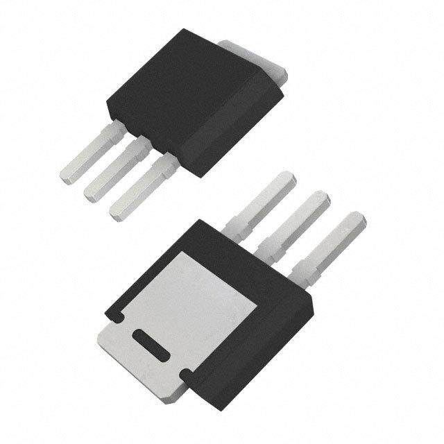
| 描述 | TRANS POWER NPN 16A 160V TO247两极晶体管 - BJT 16A 160V 125W NPN |
| 产品分类 | 晶体管(BJT) - 单路分离式半导体 |
| 品牌 | ON Semiconductor |
| 产品手册 | |
| 产品图片 |
|
| rohs | 符合RoHS无铅 / 符合限制有害物质指令(RoHS)规范要求 |
| 产品系列 | 晶体管,两极晶体管 - BJT,ON Semiconductor MJE4343G- |
| 数据手册 | |
| 产品型号 | MJE4343G |
| PCN封装 | |
| 不同 Ib、Ic时的 Vce饱和值(最大值) | 3.5V @ 2A,16A |
| 不同 Ic、Vce 时的DC电流增益(hFE)(最小值) | 15 @ 8A,2V |
| 产品目录页面 | |
| 产品种类 | 两极晶体管 - BJT |
| 供应商器件封装 | TO-247 |
| 其它名称 | MJE4343GOS |
| 功率-最大值 | 125W |
| 包装 | 管件 |
| 发射极-基极电压VEBO | 7 V |
| 商标 | ON Semiconductor |
| 增益带宽产品fT | 1 MHz |
| 安装类型 | 通孔 |
| 安装风格 | Through Hole |
| 封装 | Tube |
| 封装/外壳 | TO-247-3 |
| 封装/箱体 | TO-247 |
| 工厂包装数量 | 30 |
| 晶体管极性 | NPN |
| 晶体管类型 | NPN |
| 最大功率耗散 | 125 W |
| 最大工作温度 | + 150 C |
| 最大直流电集电极电流 | 16 A |
| 最小工作温度 | - 65 C |
| 标准包装 | 30 |
| 电压-集射极击穿(最大值) | 160V |
| 电流-集电极(Ic)(最大值) | 16A |
| 电流-集电极截止(最大值) | 750µA |
| 直流集电极/BaseGainhfeMin | 15 |
| 系列 | MJE4343 |
| 配置 | Single |
| 集电极—发射极最大电压VCEO | 160 V |
| 集电极—基极电压VCBO | 160 V |
| 集电极—射极饱和电压 | 3.5 V |
| 集电极连续电流 | 16 A |
| 频率-跃迁 | 1MHz |


- 商务部:美国ITC正式对集成电路等产品启动337调查
- 曝三星4nm工艺存在良率问题 高通将骁龙8 Gen1或转产台积电
- 太阳诱电将投资9.5亿元在常州建新厂生产MLCC 预计2023年完工
- 英特尔发布欧洲新工厂建设计划 深化IDM 2.0 战略
- 台积电先进制程称霸业界 有大客户加持明年业绩稳了
- 达到5530亿美元!SIA预计今年全球半导体销售额将创下新高
- 英特尔拟将自动驾驶子公司Mobileye上市 估值或超500亿美元
- 三星加码芯片和SET,合并消费电子和移动部门,撤换高东真等 CEO
- 三星电子宣布重大人事变动 还合并消费电子和移动部门
- 海关总署:前11个月进口集成电路产品价值2.52万亿元 增长14.8%


PDF Datasheet 数据手册内容提取
MJE4343 (NPN), MJE4353 (PNP) High-Voltage - High Power Transistors ...designed for use in high power audio amplifier applications and high voltage switching regulator circuits. http://onsemi.com Features • 16 AMPS High Collector−Emitter Sustaining Voltage − NPN PNP POWER TRANSISTORS VCEO(sus) = 160 Vdc − MJE4343 MJE4353 COMPLEMENTARY • High DC Current Gain − @ I = 8.0 Adc h = 35 (Typ) C FE SILICON • Low Collector−Emitter Saturation Voltage − 160 VOLTS V = 2.0 Vdc (Max) @ I CE(sat) C = 8.0 Adc • These are Pb−Free Devices 4 MAXIMUM RATINGS SOT−93 CASE 340D Rating Symbol Max Unit STYLE 1 Collector−Emitter Voltage VCEO 160 Vdc 1 Collector−Base Voltage VCB 160 Vdc 2 Emitter−Base Voltage VEB 7.0 Vdc 3 Collector Current − IC Adc Continuous 16 TO−247 Peak (Note 1) 20 CASE 340L STYLE 3 Base Current − Continuous IB 5.0 Adc Total Power Dissipation @ TC PD 125 Watts = 25°C Operating and Storage Junc- TJ, Tstg –65 to +150 °C NOTE: Effective June 2012 this device will tion be available only in the TO−247 Temperature Range package. Reference FPCN# 16827. THERMAL CHARACTERISTICS Characteristic Symbol Max Unit Thermal Resistance, Junction R(cid:2)JC 1.0 °C/W to Case ORDERING INFORMATION 1. Pulse Test: Pulse Width (cid:2) 5.0 (cid:3)s, Duty Cycle (cid:3) 10%. See detailed ordering and shipping information in the package dimensions section on page 2 of this data sheet. © Semiconductor Components Industries, LLC, 2012 1 Publication Order Number: May, 2012 − Rev. 5 MJE4343/D
MJE4343 (NPN), MJE4353 (PNP) MARKING DIAGRAMS TO−247 SOT−93 MJE43x3 AYWWG AYWWG MJE43x3 G 1 BASE 3 EMITTER 1 BASE 3 EMITTER 2 COLLECTOR 2 COLLECTOR MJE43x3 =Device Code A =Assembly Location Y =Year WW =Work Week G =Pb−Free Package ORDERING INFORMATION Device Order Number Package Type Shipping MJE4343G SOT−93 30 Units / Rail (Pb−Free) MJE4353G SOT−93 30 Units / Rail (Pb−Free) MJE4343G TO−247 30 Units / Rail (Pb−Free) MJE4353G TO−247 30 Units / Rail (Pb−Free) 3.5 S) T T A 3.0 W ON ( 2.5 TI A SIP 2.0 S DI R 1.5 E W O 1.0 P , D P 0.5 0 25 50 75 100 125 150 TA, AMBIENT TEMPERATURE (°C) Figure 1. Power Derating Reference: Ambient Temperature http://onsemi.com 2
MJE4343 (NPN), MJE4353 (PNP) ÎÎÎÎÎÎÎÎÎÎÎÎÎÎÎÎÎÎÎÎÎÎÎÎÎÎÎÎÎÎÎÎÎ ÎÎEÎÎLEÎÎCTRÎÎICAÎÎL CÎÎHAÎÎRACÎÎTEÎÎRISÎÎTICÎÎS (TÎÎC = 2ÎÎ5°CÎÎ unleÎÎss oÎÎtherÎÎwiseÎÎ notÎÎed) ÎÎÎÎÎÎÎÎÎÎÎÎÎÎÎÎÎÎÎÎÎÎÎÎÎÎÎÎÎÎÎÎ ÎÎÎÎÎÎÎÎÎÎÎÎÎÎÎÎÎÎÎÎChÎÎaraÎÎcteriÎÎsticÎÎÎÎÎÎÎÎÎÎÎÎÎÎÎÎÎÎÎÎÎSyÎÎmboÎÎl ÎÎÎÎÎMinÎÎÎÎÎMÎÎax ÎÎÎÎÎUniÎÎt ÎÎÎÎOFFÎÎ CHAÎÎRAÎÎCTEÎÎRISTÎÎICSÎÎÎÎÎÎÎÎÎÎÎÎÎÎÎÎÎÎÎÎÎÎÎÎÎÎÎÎÎÎÎÎÎÎÎÎÎÎÎÎÎÎÎÎÎÎÎÎÎÎÎÎÎÎÎÎ ÎÎCoÎllectoÎr−EÎmitteÎr SuÎstainÎing ÎVoltaÎge (ÎNoteÎ 2)ÎÎÎÎÎÎÎÎÎÎÎÎVCEÎO(suÎs) ÎÎÎÎÎÎÎÎÎÎVdcÎ (IC = 200 mAdc, IB = 0) 160 − ÎÎÎÎÎÎÎÎÎÎÎÎÎÎÎÎÎÎÎÎÎÎÎÎÎÎÎÎÎÎÎÎÎÎÎÎÎÎÎÎÎÎÎÎÎÎÎÎÎÎÎÎÎÎÎÎÎÎÎÎÎÎÎÎÎÎÎÎÎÎÎÎÎÎ Collector−Emitter Cutoff Current ICEO (cid:3)Adc ÎÎÎÎ(ÎÎVCEÎÎ = 80ÎÎ VdcÎÎ, IB ÎÎ= 0)ÎÎÎÎÎÎÎÎÎÎÎÎÎÎÎÎÎÎÎÎÎÎÎÎÎÎÎÎÎÎÎÎÎÎÎÎÎÎÎÎÎÎÎÎ− ÎÎÎÎÎÎ7ÎÎ50 ÎÎÎÎÎÎÎÎ ÎÎCoÎllectoÎr−EÎmitteÎr CuÎtoff ÎCurrÎent ÎÎÎÎÎÎÎÎÎÎÎÎÎÎÎIÎCEXÎÎÎÎ− ÎÎÎ1Î.0 ÎÎÎmAdÎc ÎÎ(ÎVCEÎ = RÎatedÎ VCBÎ, VEÎB(off)Î = 1.Î5 VdÎc) ÎÎÎÎÎÎÎÎÎÎÎÎÎÎÎÎÎÎ− ÎÎÎ5Î.0 ÎÎÎÎ (VCE = Rated VCB, VEB(off) = 1.5 Vdc, TC = 150°C) ÎÎÎÎÎÎÎÎÎÎÎÎÎÎÎÎÎÎÎÎÎÎÎÎÎÎÎÎÎÎÎÎÎÎÎÎÎÎÎÎÎÎÎÎÎÎÎÎÎÎÎÎÎÎÎÎÎÎÎÎÎÎÎÎÎÎÎÎÎÎÎÎÎÎ Collector−Base Cutoff Current ICBO − 750 (cid:3)Adc ÎÎÎÎ(ÎÎVCBÎÎ = RÎÎatedÎÎ VCBÎÎ, IE =ÎÎ 0)ÎÎÎÎÎÎÎÎÎÎÎÎÎÎÎÎÎÎÎÎÎÎÎÎÎÎÎÎÎÎÎÎÎÎÎÎÎÎÎÎÎÎÎÎÎÎÎÎÎÎÎÎÎÎÎÎÎÎ ÎÎEmÎitterÎ−BasÎe CÎutoffÎ CurÎrentÎÎÎÎÎÎÎÎÎÎÎÎÎÎÎÎIÎEBOÎÎÎÎ− ÎÎÎ1Î.0 ÎÎÎmAdÎc ÎÎÎÎ(ÎÎVBEÎÎ = 7.ÎÎ0 VdÎÎc, ICÎÎ = 0)ÎÎÎÎÎÎÎÎÎÎÎÎÎÎÎÎÎÎÎÎÎÎÎÎÎÎÎÎÎÎÎÎÎÎÎÎÎÎÎÎÎÎÎÎÎÎÎÎÎÎÎÎÎÎÎÎ ÎÎÎÎON CÎÎHAÎÎRACÎÎTERÎÎISTÎÎICS ÎÎ(NotÎÎe 2)ÎÎÎÎÎÎÎÎÎÎÎÎÎÎÎÎÎÎÎÎÎÎÎÎÎÎÎÎÎÎÎÎÎÎÎÎÎÎÎÎÎÎÎÎÎÎÎÎÎÎÎÎ ÎÎDCÎ CurÎrentÎ GainÎÎÎÎÎÎÎÎÎÎÎÎÎÎÎÎÎÎÎÎhFEÎÎÎÎÎÎÎÎÎÎÎ−Î (IC = 8.0 Adc, VCE = 2.0 Vdc) 15 35 (Typ) ÎÎ(ÎIC =Î 16 AÎdc, ÎVCE Î= 4.Î0 VdÎc) ÎÎÎÎÎÎÎÎÎÎÎÎÎÎÎÎÎÎÎÎ8.0ÎÎÎ15 (ÎTyp)ÎÎÎÎ ÎÎÎÎÎÎÎÎÎÎÎÎÎÎÎÎÎÎÎÎÎÎÎÎÎÎÎÎÎÎÎÎÎÎÎÎÎÎÎÎÎÎÎÎÎÎÎÎÎÎÎÎÎÎÎÎÎÎÎÎÎÎÎÎÎÎÎÎÎÎÎÎÎÎ Collector−Emitter Saturation Voltage VCE(sat) Vdc ÎÎ(ÎIC =Î 8.0 ÎAdc,Î IB =Î 800Î mA)ÎÎÎÎÎÎÎÎÎÎÎÎÎÎÎÎÎÎÎÎÎ− ÎÎÎ2Î.0 ÎÎÎÎ (IC = 16 Adc, IB = 2.0 Adc) − 3.5 ÎÎÎÎÎÎÎÎÎÎÎÎÎÎÎÎÎÎÎÎÎÎÎÎÎÎÎÎÎÎÎÎÎÎÎÎÎÎÎÎÎÎÎÎÎÎÎÎÎÎÎÎÎÎÎÎÎÎÎÎÎÎÎÎÎÎÎÎÎÎÎÎÎÎ ÎÎBaÎse−EÎmittÎer SÎaturaÎtionÎ VoltÎageÎÎÎÎÎÎÎÎÎÎÎÎÎÎÎVBÎE(saÎt) ÎÎÎ− ÎÎÎ3Î.9 ÎÎÎVdcÎ (IC = 16 Adc, IB = 2.0 Adc) ÎÎÎÎÎÎÎÎÎÎÎÎÎÎÎÎÎÎÎÎÎÎÎÎÎÎÎÎÎÎÎÎÎÎÎÎÎÎÎÎÎÎÎÎÎÎÎÎÎÎÎÎÎÎÎÎÎÎÎÎÎÎÎÎÎÎÎÎÎÎÎÎÎÎ Base−Emitter On Voltage VBE(on) − 3.9 Vdc ÎÎÎÎ(ÎÎIC =ÎÎ 16 AÎÎdc, ÎÎVCE ÎÎ= 4.ÎÎ0 VdÎÎc) ÎÎÎÎÎÎÎÎÎÎÎÎÎÎÎÎÎÎÎÎÎÎÎÎÎÎÎÎÎÎÎÎÎÎÎÎÎÎÎÎÎÎÎÎÎÎÎÎÎÎÎÎ ÎÎÎÎDYNÎÎAMIÎÎC CHÎÎARÎÎACTÎÎERIÎÎSTICÎÎS ÎÎÎÎÎÎÎÎÎÎÎÎÎÎÎÎÎÎÎÎÎÎÎÎÎÎÎÎÎÎÎÎÎÎÎÎÎÎÎÎÎÎÎÎÎÎÎÎÎÎÎÎ ÎÎCuÎrrentÎ−GaÎin − ÎBanÎdwidÎth PÎroduÎct (NÎote Î3) ÎÎÎÎÎÎÎÎÎÎÎÎÎfT ÎÎÎÎ1.0ÎÎÎÎ− ÎÎÎMHzÎ ÎÎÎÎ(ÎÎIC =ÎÎ 1.0 ÎÎAdc,ÎÎ VCEÎÎ = 2ÎÎ0 VdÎÎc, fteÎÎst = ÎÎ0.5 MÎÎHz)ÎÎÎÎÎÎÎÎÎÎÎÎÎÎÎÎÎÎÎÎÎÎÎÎÎÎÎÎÎÎÎÎÎÎÎÎÎÎÎÎÎÎÎÎÎÎÎÎÎÎ ÎÎOuÎtput ÎCapÎacitaÎnceÎÎÎÎÎÎÎÎÎÎÎÎÎÎÎÎÎÎÎCobÎÎÎÎ− ÎÎÎ8Î00 ÎÎÎpFÎ (VCB = 10 Vdc, IE = 0, f = 0.1 MHz) ÎÎÎÎÎÎÎÎÎÎÎÎÎÎÎÎÎÎÎÎÎÎÎÎÎÎÎÎÎÎÎÎÎÎÎÎÎ 2. Pulse Test: Pulse Width (cid:2) 300 (cid:3)s, Duty Cycle (cid:3) 2.0%. 3. fT = ⎪hfe⎪• ftest. http://onsemi.com 3
MJE4343 (NPN), MJE4353 (PNP) VCC +(cid:4)30 V 3.0 2.0 TJ = 25°C 25 (cid:3)s RC 1.0 IVCC/IEB == 3100 V +11 V RB SCOPE 0.7 0 s) 0.5 tr μ(cid:2)(cid:3) -(cid:4)9.0 V 51 D1 ME ( 0.3 TI 0.2 tr, tf ≤ 10 ns -(cid:4)4 V t, DUTY CYCLE = 1.0% 0.1 RB and RC VARIED TO OBTAIN DESIRED CURRENT LEVELS 0.07 td @ VBE(off) = 5.0 V (cid:5)D1 MUST BE FAST RECOVERY TYPE, e.g.: 0.05 (cid:5)(cid:5)1N5825 USED ABOVE IB ≈ 100 mA (cid:5)(cid:5)MSD6100 USED BELOW IB ≈ 100 mA 0.03 0.2 0.3 0.5 0.7 1.0 2.0 3.0 5.0 7.0 10 20 Note: Reverse polarities to test PNP devices. IC, COLLECTOR CURRENT (AMP) Figure 2. Switching Times Test Circuit Figure 3. Typical Turn−On Time TYPICAL CHARACTERISTICS 5.0 2.0 TJ = 25°C TJ = 25°C IC/IB = 10 3.0 ts IB1 = IB2 1.6 VCE = 30 V S) T L μE ((cid:2)(cid:3)s) 2.0 GE (VO 1.2 M A t, TI OLT 0.8 VBE(sat) @ IC/IB = 10 V 1.0 V, VBE @ VCE = 2.0 V tf 0.4 0.7 VCE(sat) @ IC/IB = 10 0.5 0 0.2 0.3 0.5 0.7 1.0 2.0 3.0 5.0 7.0 10 20 0.2 0.3 0.5 0.7 1.0 2.0 3.0 5.0 7.0 10 20 IC, COLLECTOR CURRENT (AMP) IC, COLLECTOR CURRENT (AMP) Figure 4. Turn−Off Time Figure 5. On Voltages http://onsemi.com 4
MJE4343 (NPN), MJE4353 (PNP) DC CURRENT GAIN 1000 1000 N N AI AI G G T T N N E E R R R 100 R 100 U U C C DC 50 VCE = 2 V DC VVCCEE = = 2 2 V V , FE TJ = 150°C , FE TTJJ = = 1 15500°°CC h 25°C h 2255°°CC 20 -(cid:4)55°C --(cid:4)5(cid:4)555°°CC 10 10 0.2 0.5 1.0 2.0 5.0 10 20 0.2 0.5 1.0 2.0 5.0 10 20 IC, COLLECTOR CURRENT (AMPS) IC, COLLECTOR CURRENT (AMPS) Figure 6. MJE4340 Series (NPN) Figure 7. MJE4350 Series (PNP) S) 2.0 T VOL TJ = 25°C E ( 1.6 G A OLT IC = 4.0 A 8.0 A 16 A V R 1.2 E T T MI -E 0.8 R O T C E L 0.4 L O C , E VC 0 0.050.07 0.1 0.2 0.3 0.5 0.7 1.0 2.0 3.0 5.0 IB, BASE CURRENT (AMP) Figure 8. Collector Saturation Region 1.0 AL D = 0.5 M 0.5 ERD) HE TZ 0.2 T LI NA 0.2 r(t), EFFECTIVE TRANSIERESISTANCE (NORM000..00.152 00.0.05SP2IUNLGSL0EE.1 0.01 (cid:2)(cid:2)DPRTJJJU EC(CCpLA( Uk=StD)) R E- 1=TV . TT0IrEM(CR°tS)C EA = (cid:2)/A I WANPJPTC( PpSM tkL1H)AY (cid:2)OX FJWCO(NtR) POWER P(pkD)UTtY1 CtY2CLE, D = t1/t2 0.01 0.02 0.05 0.1 0.2 0.5 1.0 2.0 5.0 10 20 50 100 200 500 1000 2000 t, TIME (ms) Figure 9. Thermal Response http://onsemi.com 5
MJE4343 (NPN), MJE4353 (PNP) 100 There are two limitations on the power handling ability of 50 a transistor: average junction temperature and second MP) breakdown. Safe operating area curves indicate IC − VCE T (A 20 5.0(cid:3)ms limits of the transistor that must be observed for reliable EN 10 operation; i.e., the transistor must not be subjected to greater R R 5.0 dc dissipation than the curves indicate. U R C The data of Figure 10 is based on TC = 25°C; TJ(pk) is O 2.0 T variable depending on power level. Second breakdown C LE 1.0 pulse limits are valid for duty cycles to 10% but must be L CO 0.5 derated when TC ≥ 25°C. Second breakdown limitations do , C SECONDARY BREAKDOWN LIMITED not derate the same as thermal limitations. Allowable I 0.2 THERMAL LIMIT TC = 25°C current at the voltages shown on Figure 10 may be found at BONDING WIRE LIMITED 0.1 any case temperature by using the appropriate curve on 3.0 5.0 7.0 10 20 30 50 70 100 150200 Figure 9. VCE, COLLECTOR-EMITTER VOLTAGE (VOLTS) Figure 10. Maximum Forward Bias Safe 20 Operating Area S) P REVERSE BIAS M A For inductive loads, high voltage and high current must be RENT ( 16 TVJB E=( o1ff0) 0≤° C5 V sustained simultaneously during turn−off, in most cases, R U C 12 with the base to emitter junction reverse biased. Under these R O conditions the collector voltage must be held to a safe level T C at or below a specific value of collector current. This can be LE 8.0 L accomplished by several means such as active clamping, RC CO snubbing, load line shaping, etc. The safe level for these , C I 4.0 devices is specified as Reverse Bias Safe Operating Area and represents the voltage−current conditions during 20 40 60 80 100 120 140 160 180 reverse biased turn−off. This rating is verified under VCE, COLLECTOR-EMITTER VOLTAGE (VOLTS) clamped conditions so that the device is never subjected to an avalanche mode. Figure 11 gives RBSOA characteristics. Figure 11. Maximum Reverse Bias Safe Operating Area http://onsemi.com 6
MJE4343 (NPN), MJE4353 (PNP) PACKAGE DIMENSIONS SOT−93 (TO−218) CASE 340D−02 ISSUE E C NOTES: 1.DIMENSIONING AND TOLERANCING PER ANSI B Q E Y14.5M, 1982. 2.CONTROLLING DIMENSION: MILLIMETER. MILLIMETERS INCHES DIM MIN MAX MIN MAX U 4 A --- 20.35 --- 0.801 A B 14.70 15.20 0.579 0.598 S L C 4.70 4.90 0.185 0.193 D 1.10 1.30 0.043 0.051 E 1.17 1.37 0.046 0.054 K 1 2 3 G 5.40 5.55 0.213 0.219 H 2.00 3.00 0.079 0.118 J 0.50 0.78 0.020 0.031 K 31.00 REF 1.220 REF L --- 16.20 --- 0.638 Q 4.00 4.10 0.158 0.161 S 17.80 18.20 0.701 0.717 U 4.00 REF 0.157 REF J V 1.75 REF 0.069 D H STYLE 1: PIN 1. BASE V 2. COLLECTOR G 3. EMITTER 4. COLLECTOR TO−247 CASE 340L−02 ISSUE F −T− NOTES: 1. DIMENSIONING AND TOLERANCING PER ANSI C Y14.5M, 1982. −B− 2. CONTROLLING DIMENSION: MILLIMETER. E MILLIMETERS INCHES U L DIM MIN MAX MIN MAX A 20.32 21.08 0.800 8.30 N 4 B 15.75 16.26 0.620 0.640 C 4.70 5.30 0.185 0.209 A −Q− D 1.00 1.40 0.040 0.055 E 1.90 2.60 0.075 0.102 1 2 3 0.63 (0.025) M T B M F 1.65 2.13 0.065 0.084 G 5.45 BSC 0.215 BSC H 1.50 2.49 0.059 0.098 P J 0.40 0.80 0.016 0.031 −Y− K 19.81 20.83 0.780 0.820 L 5.40 6.20 0.212 0.244 K N 4.32 5.49 0.170 0.216 P --- 4.50 --- 0.177 Q 3.55 3.65 0.140 0.144 U 6.15 BSC 0.242 BSC W 2.87 3.12 0.113 0.123 W J F2 PL H STYPLINE 13.:BASE G 2.COLLECTOR D3 PL 3.EMITTER 4.COLLECTOR 0.25 (0.010) M Y Q S http://onsemi.com 7
MJE4343 (NPN), MJE4353 (PNP) ON Semiconductor and are registered trademarks of Semiconductor Components Industries, LLC (SCILLC). SCILLC reserves the right to make changes without further notice to any products herein. SCILLC makes no warranty, representation or guarantee regarding the suitability of its products for any particular purpose, nor does SCILLC assume any liability arising out of the application or use of any product or circuit, and specifically disclaims any and all liability, including without limitation special, consequential or incidental damages. “Typical” parameters which may be provided in SCILLC data sheets and/or specifications can and do vary in different applications and actual performance may vary over time. All operating parameters, including “Typicals” must be validated for each customer application by customer’s technical experts. SCILLC does not convey any license under its patent rights nor the rights of others. SCILLC products are not designed, intended, or authorized for use as components in systems intended for surgical implant into the body, or other applications intended to support or sustain life, or for any other application in which the failure of the SCILLC product could create a situation where personal injury or death may occur. Should Buyer purchase or use SCILLC products for any such unintended or unauthorized application, Buyer shall indemnify and hold SCILLC and its officers, employees, subsidiaries, affiliates, and distributors harmless against all claims, costs, damages, and expenses, and reasonable attorney fees arising out of, directly or indirectly, any claim of personal injury or death associated with such unintended or unauthorized use, even if such claim alleges that SCILLC was negligent regarding the design or manufacture of the part. SCILLC is an Equal Opportunity/Affirmative Action Employer. This literature is subject to all applicable copyright laws and is not for resale in any manner. PUBLICATION ORDERING INFORMATION LITERATURE FULFILLMENT: N. American Technical Support: 800−282−9855 Toll Free ON Semiconductor Website: www.onsemi.com Literature Distribution Center for ON Semiconductor USA/Canada P.O. Box 5163, Denver, Colorado 80217 USA Europe, Middle East and Africa Technical Support: Order Literature: http://www.onsemi.com/orderlit Phone: 303−675−2175 or 800−344−3860 Toll Free USA/Canada Phone: 421 33 790 2910 Fax: 303−675−2176 or 800−344−3867 Toll Free USA/Canada Japan Customer Focus Center For additional information, please contact your local Email: orderlit@onsemi.com Phone: 81−3−5817−1050 Sales Representative http://onsemi.com MJE4343/D 8