ICGOO在线商城 > 分立半导体产品 > 晶体管 - UGBT,MOSFET - 单 > FGA60N60UFDTU

 Datasheet下载
- 型号: FGA60N60UFDTU
- 制造商: Fairchild Semiconductor
- 库位|库存: xxxx|xxxx
- 要求:
| 数量阶梯 | 香港交货 | 国内含税 |
| +xxxx | $xxxx | ¥xxxx |
查看当月历史价格
查看今年历史价格
FGA60N60UFDTU产品简介:
ICGOO电子元器件商城为您提供FGA60N60UFDTU由Fairchild Semiconductor设计生产,在icgoo商城现货销售,并且可以通过原厂、代理商等渠道进行代购。 FGA60N60UFDTU价格参考。Fairchild SemiconductorFGA60N60UFDTU封装/规格:晶体管 - UGBT,MOSFET - 单, IGBT Field Stop 600V 120A 298W Through Hole TO-3P。您可以下载FGA60N60UFDTU参考资料、Datasheet数据手册功能说明书,资料中有FGA60N60UFDTU 详细功能的应用电路图电压和使用方法及教程。
ON Semiconductor的FGA60N60UFDTU是一款MOSFET(金属氧化物半导体场效应晶体管),属于超结MOSFET(Ultrafast Recovery MOSFET, UGBT)系列,适用于多种高压、高效率电力电子应用。以下是其主要应用场景:

1. 开关电源 (SMPS):
   FGA60N60UFDTU的高电压耐受能力(600V击穿电压)和低导通电阻(Rds(on)约为0.18Ω)使其非常适合用于开关电源中的功率转换电路,如AC-DC或DC-DC转换器。

2. 电机驱动:
   该器件可应用于各种电机驱动场景,例如家用电器(如洗衣机、空调)、工业设备和电动工具的无刷直流电机(BLDC)驱动器中,提供高效的开关性能和可靠的运行。

3. 太阳能逆变器:
   在光伏系统中,FGA60N60UFDTU可用于逆变器的功率级,实现高效的能量转换,将直流电转换为交流电并接入电网或负载。

4. 电动车/混合动力车 (EV/HEV):
   该MOSFET可以用于电动车的车载充电器、DC-DC转换器以及辅助系统的功率控制模块,支持高效率的能量管理。

5. PFC(功率因数校正)电路:
   在需要提高功率因数的应用中,这款MOSFET能够作为主开关器件,帮助实现更高效的PFC功能,减少谐波失真。

6. 不间断电源 (UPS):
   FGA60N60UFDTU适用于UPS系统的逆变和整流部分,确保在市电中断时提供稳定可靠的备用电源输出。

7. LED驱动器:
   在大功率LED照明应用中,此MOSFET可用于恒流或恒压驱动电路,以实现高效且稳定的LED亮度控制。

总结来说,FGA60N60UFDTU凭借其卓越的电气特性(如低栅极电荷、快速开关速度和高能效),广泛适用于需要高电压、高频率及低损耗的各类功率转换和控制场景。
| 参数 | 数值 |
| 25°C时Td(开/关)值 | 23ns/130ns |
| 产品目录 | |
| Current-CollectorPulsed(Icm) | 180A |
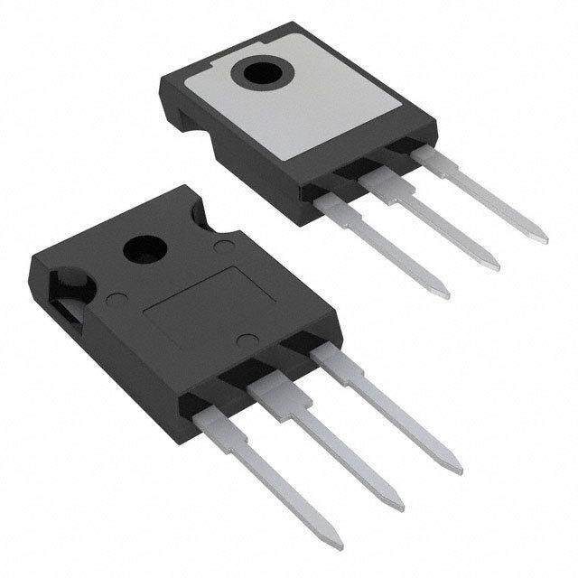
| 描述 | IGBT 600V 120A 298W TO3PIGBT 晶体管 600V 60A FIELD STOP |
| 产品分类 | IGBT - 单路分离式半导体 |
| GateCharge | 188nC |
| IGBT类型 | 场截止 |
| 品牌 | Fairchild Semiconductor |
| 产品手册 | |
| 产品图片 |
|
| rohs | 符合RoHS无铅 / 符合限制有害物质指令(RoHS)规范要求 |
| 产品系列 | 晶体管,IGBT 晶体管,Fairchild Semiconductor FGA60N60UFDTU- |
| 数据手册 | |
| 产品型号 | FGA60N60UFDTU |
| PCN设计/规格 | |
| SwitchingEnergy | 1.81mJ (开), 810µJ (关) |
| TestCondition | 400V, 60A, 5 欧姆, 15V |
| 不同 Vge、Ic时的 Vce(on) | 2.4V @ 15V,60A |
| 产品目录页面 | |
| 产品种类 | IGBT 晶体管 |
| 供应商器件封装 | TO-3PN |
| 功率-最大值 | 298W |
| 包装 | 管件 |
| 单位重量 | 6.401 g |
| 反向恢复时间(trr) | 47ns |
| 商标 | Fairchild Semiconductor |
| 在25C的连续集电极电流 | 120 A |
| 安装类型 | 通孔 |
| 安装风格 | Through Hole |
| 封装 | Tube |
| 封装/外壳 | TO-3P-3,SC-65-3 |
| 工厂包装数量 | 30 |
| 最大工作温度 | + 150 C |
| 最小工作温度 | - 55 C |
| 栅极/发射极最大电压 | +/- 20 V |
| 标准包装 | 30 |
| 电压-集射极击穿(最大值) | 600V |
| 电流-集电极(Ic)(最大值) | 120A |
| 系列 | FGA60N60UFDTU |
| 输入类型 | 标准 |
| 配置 | Single |
| 集电极—发射极最大电压VCEO | 600 V |


- 商务部:美国ITC正式对集成电路等产品启动337调查
- 曝三星4nm工艺存在良率问题 高通将骁龙8 Gen1或转产台积电
- 太阳诱电将投资9.5亿元在常州建新厂生产MLCC 预计2023年完工
- 英特尔发布欧洲新工厂建设计划 深化IDM 2.0 战略
- 台积电先进制程称霸业界 有大客户加持明年业绩稳了
- 达到5530亿美元!SIA预计今年全球半导体销售额将创下新高
- 英特尔拟将自动驾驶子公司Mobileye上市 估值或超500亿美元
- 三星加码芯片和SET,合并消费电子和移动部门,撤换高东真等 CEO
- 三星电子宣布重大人事变动 还合并消费电子和移动部门
- 海关总署:前11个月进口集成电路产品价值2.52万亿元 增长14.8%


PDF Datasheet 数据手册内容提取
Is Now Part of To learn more about ON Semiconductor, please visit our website at www.onsemi.com Please note: As part of the Fairchild Semiconductor integration, some of the Fairchild orderable part numbers will need to change in order to meet ON Semiconductor’s system requirements. Since the ON Semiconductor product management systems do not have the ability to manage part nomenclature that utilizes an underscore (_), the underscore (_) in the Fairchild part numbers will be changed to a dash (-). This document may contain device numbers with an underscore (_). Please check the ON Semiconductor website to verify the updated device numbers. The most current and up-to-date ordering information can be found at www.onsemi.com. Please email any questions regarding the system integration to Fairchild_questions@onsemi.com. ON Semiconductor and the ON Semiconductor logo are trademarks of Semiconductor Components Industries, LLC dba ON Semiconductor or its subsidiaries in the United States and/or other countries. ON Semiconductor owns the rights to a number of patents, trademarks, copyrights, trade secrets, and other intellectual property. A listing of ON Semiconductor’s product/patent coverage may be accessed at www.onsemi.com/site/pdf/Patent-Marking.pdf. ON Semiconductor reserves the right to make changes without further notice to any products herein. ON Semiconductor makes no warranty, representation or guarantee regarding the suitability of its products for any particular purpose, nor does ON Semiconductor assume any liability arising out of the application or use of any product or circuit, and specifically disclaims any and all liability, including without limitation special, consequential or incidental damages. Buyer is responsible for its products and applications using ON Semiconductor products, including compliance with all laws, regulations and safety requirements or standards, regardless of any support or applications information provided by ON Semiconductor. “Typical” parameters which may be provided in ON Semiconductor data sheets and/or specifications can and do vary in different applications and actual performance may vary over time. All operating parameters, including “Typicals” must be validated for each customer application by customer’s technical experts. ON Semiconductor does not convey any license under its patent rights nor the rights of others. ON Semiconductor products are not designed, intended, or authorized for use as a critical component in life support systems or any FDA Class 3 medical devices or medical devices with a same or similar classification in a foreign jurisdiction or any devices intended for implantation in the human body. Should Buyer purchase or use ON Semiconductor products for any such unintended or unauthorized application, Buyer shall indemnify and hold ON Semiconductor and its officers, employees, subsidiaries, affiliates, and distributors harmless against all claims, costs, damages, and expenses, and reasonable attorney fees arising out of, directly or indirectly, any claim of personal injury or death associated with such unintended or unauthorized use, even if such claim alleges that ON Semiconductor was negligent regarding the design or manufacture of the part. ON Semiconductor is an Equal Opportunity/Affirmative Action Employer. This literature is subject to all applicable copyright laws and is not for resale in any manner.
F G A March 2015 6 0 N 6 FGA60N60UFD 0 U 600 V, 60 A Field Stop IGBT F D — Features General Description 6 0 • High Current Capability Using novel field stop IGBT technology, Fairchild’s field stop 0 • Low Saturation Voltage: VCE(sat) = 1.9 V @ IC = 60 A IwGeBldTesr oafnfedr PthFeC oapptpimlicuamtio pnesr fwohrmeraen lcoew focor nsdoulacrt ioinnv aenrtde rs, wUitPcSh-, V, 6 • High Input Impedance ing losses are essential. 0 • Fast Switching A • RoHS Compliant F i Applications e l d • Solar Inverter, UPS, Welder, PFC S t o p I G B T C G TO-3P E G C E Absolute Maximum Ratings Symbol Description Ratings Unit V Collector to Emitter Voltage 600 V CES Gate to Emitter Voltage ±20 V V GES Transient Gate-to-Emitter Voltage ±30 Collector Current @ T = 25oC 120 A I C C Collector Current @ T = 100oC 60 A C ICM (1) Pulsed Collector Current @ TC = 25oC 180 A Maximum Power Dissipation @ T = 25oC 298 W P C D Maximum Power Dissipation @ T = 100oC 119 W C T Operating Junction Temperature -55 to +150 oC J T Storage Temperature Range -55 to +150 oC stg Maximum Lead Temp. for soldering TL Purposes, 1/8” from case for 5 seconds 300 oC Notes: 1: Repetitive test , Pulse width limited by max. junction temperature Thermal Characteristics Symbol Parameter Typ. Max. Unit RJC(IGBT) Thermal Resistance, Junction to Case - 0.33 oC/W RJC(Diode) Thermal Resistance, Junction to Case - 1.1 oC/W RJA Thermal Resistance, Junction to Ambient - 40 oC/W ©2009 Fairchild Semiconductor Corporation 1 www.fairchildsemi.com FGA60N60UFD Rev. 1.4
F G Package Marking and Ordering Information A 6 0 Part Number Top Mark Package Packing Method Reel Size Tape Width Quantity N 6 FGA60N60UFDTU FGA60N60UFD TO-3P Tube N/A N/A 30 0 U F Electrical Characteristics of the IGBT D TC = 25°C unless otherwise noted — Symbol Parameter Test Conditions Min. Typ. Max. Unit 6 0 0 Off Characteristics V , BVCES Collector to Emitter Breakdown Voltage VGE = 0 V, IC = 250 A 600 - - V 6 0 BTVCES TVeomltapgeerature Coefficient of Breakdown VGE = 0 V, IC = 250 A - 0.67 - V/oC A J F I Collector Cut-Off Current V = V , V = 0 V - - 250 A i CES CE CES GE e l I G-E Leakage Current V = V , V = 0 V - - ±400 nA d GES GE GES CE S t On Characteristics o p VGE(th) G-E Threshold Voltage IC = 250 A, VCE = VGE 4.0 5.0 6.5 V IG IC = 60 A, VGE = 15 V - 1.9 2.4 V B V Collector to Emitter Saturation Voltage T CE(sat) ITC = = 6 102 A5,o VCGE = 15 V, - 2.1 - V C Dynamic Characteristics C Input Capacitance - 2855 - pF ies V = 30 VV = 0 V, C Output Capacitance CE , GE - 325 - pF oes f = 1 MHz C Reverse Transfer Capacitance - 110 - pF res Switching Characteristics t Turn-On Delay Time - 23 - ns d(on) t Rise Time - 58 - ns r td(off) Turn-Off Delay Time VCC = 400 V, IC = 60 A, - 130 - ns tEf FTuarlln T-Oimne Switching Loss IRnGd u=c t5iv e ,L VoGaEd ,= T 1C5 = V 2,5oC -- 14.801 8-0 mnsJ on E Turn-Off Switching Loss - 0.81 - mJ off E Total Switching Loss - 2.62 - mJ ts t Turn-On Delay Time - 22 - ns d(on) t Rise Time - 61 - ns r td(off) Turn-Off Delay Time VCC = 400 V, IC = 60 A, - 141 - ns tEf FTuarlln T-Oimne Switching Loss IRnGd u=c t5iv e ,L VoGaEd ,= T 1C5 = V 1,25oC -- 16.932 -- mnsJ on E Turn-Off Switching Loss - 1.23 - mJ off E Total Switching Loss - 3.15 - mJ ts Q Total Gate Charge - 188 - nC g V = 400 V, I = 60 A, Q Gate to Emitter Charge CE C - 21 - nC ge VGE = 15 V Q Gate to Collector Charge - 97 - nC gc ©2009 Fairchild Semiconductor Corporation 2 www.fairchildsemi.com FGA60N60UFD Rev. 1.4
F G Electrical Characteristics of the Diode TC = 25°C unless otherwise noted A 6 Symbol Parameter Test Conditions Min. Typ. Max Unit 0 N T = 25oC - 2.0 2.6 6 V Diode Forward Voltage I = 30 A C V 0 FM F T = 125oC - 1.8 - U C F T = 25oC - 47 - D trr Diode Reverse Recovery Time TC = 125oC - 179 - ns — IF = 30 A, diF/dt = 200 A/s TC = 25oC - 83 - 6 Q Diode Reverse Recovery Charge C nC 0 rr T = 125oC - 567 - 0 C V , 6 0 A F i e l d S t o p I G B T ©2009 Fairchild Semiconductor Corporation 3 www.fairchildsemi.com FGA60N60UFD Rev. 1.4
F G Typical Performance Characteristics A 6 0 N Figure 1. Typical Output Characteristics Figure 2. Typical Output Characteristics 6 0 180 180 U TC = 25oC TC = 125oC F 150 20V 15V 150 20V 15V D — A] 12V A] 12V nt, I [C 120 10V nt, I [C 120 10V 600 or Curre 90 or Curre 90 V, 60 Collect 3600 VGE = 8V Collect 3600 VGE = 8V A Fie l d 0 0 S 0 2 4 6 8 0 2 4 6 8 to Collector-Emitter Voltage, VCE [V] Collector-Emitter Voltage, VCE [V] p I G Figure 3. Typical Saturation Voltage Figure 4. Transfer Characteristics B T Characteristics 180 180 Common Emitter Common Emitter 150 VGE = 15V 150 VCE = 20V nt, I [A]C 120 TTCC == 2152o5CoC ent, I [A]C 120 TTCC == 2152o5CoC urre 90 Curr 90 ctor C 60 ector 60 olle Coll C 30 30 0 0 0 1 2 3 4 5 0 1 2 3 4 5 Collector-Emitter Voltage, VCE [V] Gate-Emitter Voltage,VGE [V] Figure 5. Saturation Voltage vs. Case Figure 6. Saturation Voltage vs. V GE Temperature at Variant Current Level 4.0 20 Common Emitter Common Emitter [V]CE 3.5 VGE = 15V [V]CE16 TC = -40oC V V e, e, g 3.0 g a a Volt 120A Volt 12 er 2.5 er mitt mitt 8 or-E 2.0 60A or-E ct ct 120A olle 1.5 olle 4 60A C C IC = 30A IC = 30A 1.0 0 25 50 75 100 125 0 3 6 9 12 15 18 Collector-EmitterCase Temperature, TC [oC] Gate-Emitter Voltage, VGE [V] ©2009 Fairchild Semiconductor Corporation 4 www.fairchildsemi.com FGA60N60UFD Rev. 1.4
F G Typical Performance Characteristics A 6 0 N Figure 7. Saturation Voltage vs. VGE Figure 8. Saturation Voltage vs. VGE 6 0 20 20 U Common Emitter Common Emitter F ctor-Emitter VoltageV [V], CE11826 60A TC1 2=0 2A5oC or-Emitter Voltage, V [V]CE11826 TC 1=2 102A5oC D — 600 V, 60 A F Colle 4 IC = 30A Collect 4 I6C0 =A 30A ield 0 0 S 0 3 6 9 12 15 18 0 3 6 9 12 15 18 to Gate-Emitter Voltage, VGE [V] Gate-Emitter Voltage, VGE [V] p I G Figure 9. Capacitance Characteristics Figure 10. Gate charge Characteristics B T 6000 15 Common Emitter Common Emitter VGE = 0V, f = 1MHz TC = 25oC Cies TC = 25oC [V]GE12 300V Capacitance [pF] 24000000 Coes mitter Voltage, V 69 VCC = 100V 200V E e- at 3 G C res 0 0 1 10 30 0 50 100 150 200 Collector-Emitter Voltage, VCE [V] Gate Charge, Qg [nC] Figure 11. SOA Characteristics Figure 12. Turn off Switching SOA Characteristics 500 300 10s 100 100 ent, I [A]c 10 110m0ss nt, I [A]C Collector Curr 0.11 SPiunlgsele T NCo =n r2e5poeCtitive 1D0C ms Collector Curre 10 Curves must be derated linearly with increase Safe Operating Area in temperature V = 15V, T = 125oC GE C 0.01 1 1 10 100 1000 1 10 100 1000 Collector-Emitter Voltage, VCE [V] Collector-Emitter Voltage, VCE [V] ©2009 Fairchild Semiconductor Corporation 5 www.fairchildsemi.com FGA60N60UFD Rev. 1.4
F G Typical Performance Characteristics A 6 0 N Figure 13. Turn-on Characteristics vs. Figure 14. Turn-off Characteristics vs. 6 Gate Resistance G ate Resistance 0 U 300 6000 F Common Emitter D VCC = 400V, VGE = 15V — IC = 60A 1000 TC = 25oC 60 ns]100 t ns] TC = 125oC 0 me [ r me [ td(off) V, g Ti g Ti 60 witchin CVCoCm =m 4o0n0 EVm, VitGteE r= 15V witchin 100 tf A Fi S td(on) ITCC = = 6 205AoC S eld TC = 125oC St 10 10 o 0 10 20 30 40 50 0 10 20 30 40 50 p Gate Resistance, RG [] Gate Resistance, RG [] IG B T Figure 15. Turn-on Characteristics vs Figure 16.Turn-off Characteristics vs. Collector Current Collector Current 500 1000 Common Emitter Common Emitter VGE = 15V, RG = 5 VGE = 15V, RG = 5 T = 25oC T = 25oC C C s] TC = 125oC tr s] TC = 125oC n n e [ 100 e [ m m Ti Ti t g g d(off) n n hi hi c c100 wit wit S S t d(on) t f 10 30 0 20 40 60 80 100 120 0 20 40 60 80 100 120 Collector Current, IC [A] Collector Current, IC [A] Figure 17. Switching Loss vs. Gate ResistanceFigure 18.Switching Loss vs. Collector Current 20 20 Common Emitter Common Emitter VCC = 400V, VGE = 15V 10 VGE = 15V, RG = 5 10 IC = 60A TC = 25oC Eon J] TC = 25oC J] TC = 125oC s [m TC = 125oC s [m Los Los Eoff ng Eon ng 1 hi hi c c wit wit S S 1 E off 0.1 0 10 20 30 40 50 0 20 40 60 80 100 120 Gate Resistance, RG [] Collector Current, IC [A] ©2009 Fairchild Semiconductor Corporation 6 www.fairchildsemi.com FGA60N60UFD Rev. 1.4
F G Typical Performance Characteristics A 6 0 N Figure 19. Forward Characteristics Figure 20. Reverse Current 6 0 200 500 U F 100 100 D TC = 125oC — ent, I [A]F TJ = 125oC TJ = 25oC nt , I [A]R 10 600 V Curr 10 urre 1 TC = 75oC , 6 ard TJ = 75oC se C 0 A orw ver F F TTC == 2152o5CoC Re 0.1 TC = 25oC ield C 1 0.01 S 0 1 2 3 4 0 200 400 600 to Forward Voltage, VF [V] Reverse Voltage, VR [V] p I G Figure 21. Stored Charge Figure 22. Reverse Recovery Time B T 120 60 s] Q [nC]rr18000 200A/s Time, t [nrr50 200A/s ge, ery Char 60 ecov di/dt = 100A/s Stored 40 diF/dt = 100A/s verse R40 e Tc = 25℃ R Tc = 25℃ 20 30 5 20 40 60 5 20 40 60 Forward Current, IF [A] Forward Current, IF [A] Figure 23. Transient Thermal Impedance of IGBT 1 c] Zthj 0.5 se [ 0.1 0.2 n po 0.1 es 0.05 R mal 0.01 00..0021 PDM Ther single pulse Duty Factor, tD1t 2= t1/t2 Peak Tj = Pdm x Zthjc + TC 1E-3 1E-5 1E-4 1E-3 0.01 0.1 1 Rectangular Pulse Duration [sec] ©2009 Fairchild Semiconductor Corporation 7 www.fairchildsemi.com FGA60N60UFD Rev. 1.4
5.00 4.60 13.80 13.40 1.65 3.30 16.20 5.20 1.45 3.10 15.40 4.80 R0.50 3° 16.96 20.10 18.90 16.56 19.70 18.50 7.20 6.80 3° 4° 1 3 2.00 3.70 1.85 1.60 3.30 2.60 2.20 2.20 20.30 1.80 3.20 19.70 2.80 1.20 0.80 0.55 M 0.75 0.55 5.45 5.45 NOTES: UNLESS OTHERWISE SPECIFIED A) THIS PACKAGE CONFORMS TO EIAJ SC-65 PACKAGING STANDARD. B) ALL DIMENSIONS ARE IN MILLIMETERS. C) DIMENSION AND TOLERANCING PER ASME14.5-2009. R0.50 D) DIMENSIONS ARE EXCLUSSIVE OF BURRS, MOLD FLASH, AND TIE BAR EXTRUSSIONS. E) DRAWING FILE NAME: TO3PN03AREV2. F) FAIRCHILD SEMICONDUCTOR.
ON Semiconductor and are trademarks of Semiconductor Components Industries, LLC dba ON Semiconductor or its subsidiaries in the United States and/or other countries. ON Semiconductor owns the rights to a number of patents, trademarks, copyrights, trade secrets, and other intellectual property. A listing of ON Semiconductor’s product/patent coverage may be accessed at www.onsemi.com/site/pdf/Patent−Marking.pdf. ON Semiconductor reserves the right to make changes without further notice to any products herein. ON Semiconductor makes no warranty, representation or guarantee regarding the suitability of its products for any particular purpose, nor does ON Semiconductor assume any liability arising out of the application or use of any product or circuit, and specifically disclaims any and all liability, including without limitation special, consequential or incidental damages. Buyer is responsible for its products and applications using ON Semiconductor products, including compliance with all laws, regulations and safety requirements or standards, regardless of any support or applications information provided by ON Semiconductor. “Typical” parameters which may be provided in ON Semiconductor data sheets and/or specifications can and do vary in different applications and actual performance may vary over time. All operating parameters, including “Typicals” must be validated for each customer application by customer’s technical experts. ON Semiconductor does not convey any license under its patent rights nor the rights of others. ON Semiconductor products are not designed, intended, or authorized for use as a critical component in life support systems or any FDA Class 3 medical devices or medical devices with a same or similar classification in a foreign jurisdiction or any devices intended for implantation in the human body. Should Buyer purchase or use ON Semiconductor products for any such unintended or unauthorized application, Buyer shall indemnify and hold ON Semiconductor and its officers, employees, subsidiaries, affiliates, and distributors harmless against all claims, costs, damages, and expenses, and reasonable attorney fees arising out of, directly or indirectly, any claim of personal injury or death associated with such unintended or unauthorized use, even if such claim alleges that ON Semiconductor was negligent regarding the design or manufacture of the part. ON Semiconductor is an Equal Opportunity/Affirmative Action Employer. This literature is subject to all applicable copyright laws and is not for resale in any manner. PUBLICATION ORDERING INFORMATION LITERATURE FULFILLMENT: N. American Technical Support: 800−282−9855 Toll Free ON Semiconductor Website: www.onsemi.com Literature Distribution Center for ON Semiconductor USA/Canada 19521 E. 32nd Pkwy, Aurora, Colorado 80011 USA Europe, Middle East and Africa Technical Support: Order Literature: http://www.onsemi.com/orderlit Phone: 303−675−2175 or 800−344−3860 Toll Free USA/Canada Phone: 421 33 790 2910 Fax: 303−675−2176 or 800−344−3867 Toll Free USA/Canada Japan Customer Focus Center For additional information, please contact your local Email: orderlit@onsemi.com Phone: 81−3−5817−1050 Sales Representative © Semiconductor Components Industries, LLC www.onsemi.com www.onsemi.com 1
Mouser Electronics Authorized Distributor Click to View Pricing, Inventory, Delivery & Lifecycle Information: O N Semiconductor: FGA60N60UFDTU