ICGOO在线商城 > 分立半导体产品 > 晶体管 - 双极 (BJT) - 单 > BC817-25,235
 Datasheet下载
- 型号: BC817-25,235
- 制造商: NXP Semiconductors
- 库位|库存: xxxx|xxxx
- 要求:
| 数量阶梯 | 香港交货 | 国内含税 |
| +xxxx | $xxxx | ¥xxxx |
查看当月历史价格
查看今年历史价格
BC817-25,235产品简介:
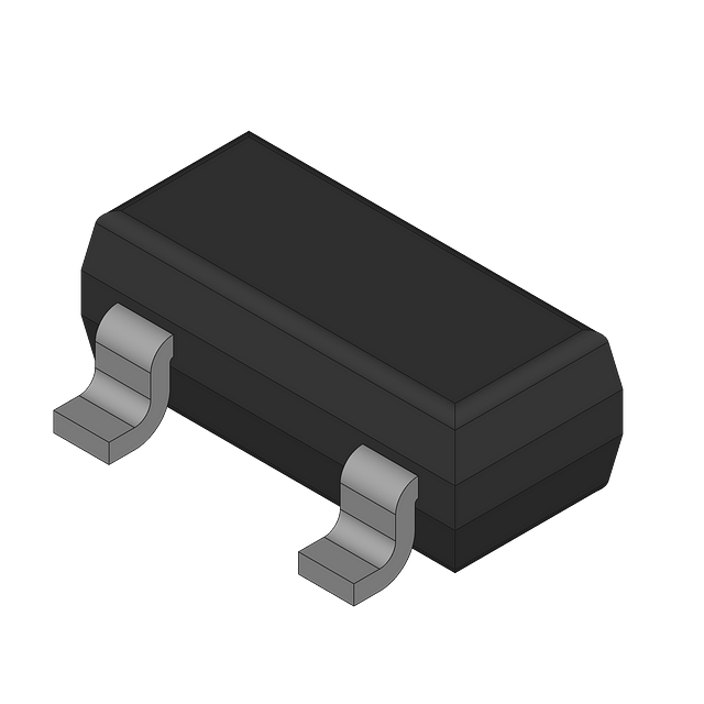
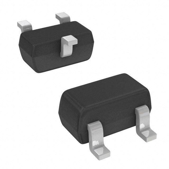
ICGOO电子元器件商城为您提供BC817-25,235由NXP Semiconductors设计生产,在icgoo商城现货销售,并且可以通过原厂、代理商等渠道进行代购。 BC817-25,235价格参考。NXP SemiconductorsBC817-25,235封装/规格:晶体管 - 双极 (BJT) - 单, Bipolar (BJT) Transistor NPN 45V 500mA 100MHz 250mW Surface Mount TO-236AB。您可以下载BC817-25,235参考资料、Datasheet数据手册功能说明书,资料中有BC817-25,235 详细功能的应用电路图电压和使用方法及教程。
Nexperia USA Inc. 的 BC817-25,235 是一款 NPN 型双极结型晶体管(BJT),广泛应用于中小功率放大和开关电路中。该器件采用 SOT-23 小型表面贴装封装,适合高密度印刷电路板设计,具有良好的热稳定性和可靠性。

BC817-25,235 的典型应用场景包括:
1. 开关电路:常用于驱动继电器、LED、小型电机及逻辑控制电路中的信号切换,因其具备较高的电流增益和快速响应能力,能高效实现低电压/低电流信号对高负载的控制。
2. 信号放大:适用于音频信号、传感器信号等小信号放大电路,如在消费类电子产品中的前置放大级。
3. 电源管理:在DC-DC转换器、稳压电路中作为通断控制元件,协助实现电压调节与电流控制。
4. 数字接口电路:用于微控制器与外围设备之间的电平转换或驱动缓冲,提升系统兼容性与驱动能力。
5. 工业与汽车电子:由于其工作温度范围宽、性能稳定,也常见于汽车电子模块(如车灯控制)、工业控制板及家用电器控制单元中。

该型号晶体管具有25至300的直流电流增益(hFE)范围,集电极电流可达500mA,适合多种通用场景。凭借Nexperia一贯的高质量标准,BC817-25,235在成本、性能与可靠性之间实现了良好平衡,是现代电子设计中常用的通用型BJT器件之一。
| 参数 | 数值 |
| 产品目录 | |
| 描述 | TRANSISTOR NPN 500MA 45V SOT23两极晶体管 - BJT TRANS GP TAPE-13 |
| 产品分类 | 晶体管(BJT) - 单路分离式半导体 |
| 品牌 | NXP Semiconductors |
| 产品手册 | |
| 产品图片 |
|
| rohs | 符合RoHS无铅 / 符合限制有害物质指令(RoHS)规范要求 |
| 产品系列 | 晶体管,两极晶体管 - BJT,NXP Semiconductors BC817-25,235- |
| 数据手册 | |
| 产品型号 | BC817-25,235 |
| PCN封装 | |
| PCN设计/规格 | |
| 不同 Ib、Ic时的 Vce饱和值(最大值) | 700mV @ 50mA,500mA |
| 不同 Ic、Vce 时的DC电流增益(hFE)(最小值) | 160 @ 100mA,1V |
| 产品种类 | 两极晶体管 - BJT |
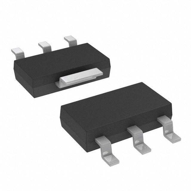
| 供应商器件封装 | SOT-23 (TO-236AB) |
| 其它名称 | 568-7991-2 |
| 功率-最大值 | 250mW |
| 包装 | 带卷 (TR) |
| 发射极-基极电压VEBO | 5 V |
| 商标 | NXP Semiconductors |
| 增益带宽产品fT | 100 MHz |
| 安装类型 | 表面贴装 |
| 安装风格 | SMD/SMT |
| 封装 | Reel |
| 封装/外壳 | TO-236-3,SC-59,SOT-23-3 |
| 封装/箱体 | SOT-23 |
| 工厂包装数量 | 10000 |
| 晶体管极性 | NPN |
| 晶体管类型 | NPN |
| 最大功率耗散 | 250 mW |
| 最大工作温度 | + 150 C |
| 最大直流电集电极电流 | 0.5 A |
| 最小工作温度 | - 65 C |
| 标准包装 | 10,000 |
| 特色产品 | http://www.digikey.com/cn/zh/ph/NXP/I2C.html |
| 电压-集射极击穿(最大值) | 45V |
| 电流-集电极(Ic)(最大值) | 500mA |
| 电流-集电极截止(最大值) | - |
| 直流电流增益hFE最大值 | 160 at 100 mA at 1 V |
| 直流集电极/BaseGainhfeMin | 160 at 100 mA at 1 V, 40 at 500 mA at 1 V |
| 配置 | Single |
| 集电极—发射极最大电压VCEO | 45 V |
| 集电极—基极电压VCBO | 50 V |
| 零件号别名 | /T3 BC817-25 |
| 频率-跃迁 | 100MHz |


- 商务部:美国ITC正式对集成电路等产品启动337调查
- 曝三星4nm工艺存在良率问题 高通将骁龙8 Gen1或转产台积电
- 太阳诱电将投资9.5亿元在常州建新厂生产MLCC 预计2023年完工
- 英特尔发布欧洲新工厂建设计划 深化IDM 2.0 战略
- 台积电先进制程称霸业界 有大客户加持明年业绩稳了
- 达到5530亿美元!SIA预计今年全球半导体销售额将创下新高
- 英特尔拟将自动驾驶子公司Mobileye上市 估值或超500亿美元
- 三星加码芯片和SET,合并消费电子和移动部门,撤换高东真等 CEO
- 三星电子宣布重大人事变动 还合并消费电子和移动部门
- 海关总署:前11个月进口集成电路产品价值2.52万亿元 增长14.8%


PDF Datasheet 数据手册内容提取
BC817 series 45 V, 500 mA NPN general-purpose transistors Rev. 7 — 18 June 2018 Product data sheet 1 Product profile 1.1 General description NPN general-purpose transistors in a small SOT23 Surface-Mounted Device (SMD) plastic package. Table 1. Product overview Type number Package PNP complement Nexperia JEDEC JEITA BC817 SOT23 TO-236AB - BC807 BC817-16 BC807-16 BC817-25 BC807-25 BC817-40 BC807-40 1.2 Features and benefits • High current • Three current gain selections • AEC-Q101 qualified 1.3 Applications • General-purpose switching and amplification
Nexperia BC817 series 45 V, 500 mA NPN general-purpose transistors 1.4 Quick reference data Table 2. Quick reference data T = 25 °C unless otherwise specified. amb Symbol Parameter Conditions Min Typ Max Unit V collector-emitter voltage open base - - 45 V CEO I collector current - - 500 mA C I peak collector current single pulse; t ≤ 1 ms - - 1 A CM p [1] h BC817 V = 1 V; I = 100 mA 100 - 600 FE CE C [1] BC817-16 100 - 250 [1] BC817-25 160 - 400 [1] BC817-40 250 - 600 [1] pulsed; tp ≤ 300 μs; δ ≤ 0.02 2 Pinning information Table 3. Pinning Pin Symbol Description Simplified outline Graphic symbol SOT23 1 B base 2 E emitter 3 C 3 C collector B E 1 2 sym123 3 Ordering information Table 4. Ordering information Type number Package Name Description Version BC817 TO-236AB Plastic surface-mounted package; 3 leads SOT23 BC817-16 BC817-25 BC817-40 BC817_SER All information provided in this document is subject to legal disclaimers. © Nexperia B.V. 2018. All rights reserved. Product data sheet Rev. 7 — 18 June 2018 2 / 15
Nexperia BC817 series 45 V, 500 mA NPN general-purpose transistors 4 Marking Table 5. Marking Type number Marking code [1] BC817 6D% [1] BC817-16 6A% [1] BC817-25 6B% [1] BC817-40 6C% [1] % = placeholder for manufacturing site code 5 Limiting values Table 6. Limiting values In accordance with the Absolute Maximum Rating System (IEC 60134). Symbol Parameter Conditions Min Max Unit V collector-base voltage open emitter - 50 V CBO V collector-emitter voltage open base - 45 V CEO V emitter-base voltage open collector - 5 V EBO I collector current - 500 mA C I peak collector current single pulse; t ≤ 1 ms - 1 A CM p I peak base current single pulse; t ≤ 1 ms - 200 mA BM p [1][2] P total power dissipation T ≤ 25 °C - 250 mW tot amb [3][2] - 345 mW T junction temperature - 150 °C j T ambient temperature -65 150 °C amb T storage temperature -65 150 °C stg [1] Device mounted on an FR4 Printed-Circuit-Board (PCB); single-sided copper; tin-plated and standard footprint. [2] Valid for all available selection groups. [3] Device mounted on an FR4 Printed-Circuit-Board (PCB); single-sided copper; tin-plated; mounting pad for collector 1 cm2. BC817_SER All information provided in this document is subject to legal disclaimers. © Nexperia B.V. 2018. All rights reserved. Product data sheet Rev. 7 — 18 June 2018 3 / 15
Nexperia BC817 series 45 V, 500 mA NPN general-purpose transistors aaa-028120 400 Ptot (1) (mW) 300 (2) 200 100 0 -75 -25 25 75 125 175 Tamb (°C) 2 (1) FR4 PCB, single-sided copper; 1 cm (2) FR4 PCB, single-sided copper; standard footprint Figure 1. Power derating curves BC817_SER All information provided in this document is subject to legal disclaimers. © Nexperia B.V. 2018. All rights reserved. Product data sheet Rev. 7 — 18 June 2018 4 / 15
Nexperia BC817 series 45 V, 500 mA NPN general-purpose transistors 6 Thermal characteristics Table 7. Thermal characteristics Symbol Parameter Conditions Min Typ Max Unit [1][2] R thermal resistance from junction in free air - - 500 K/W th(j-a) to ambient [3][2] - - 362 K/W [1] Device mounted on an FR4 Printed-Circuit-Board (PCB); single-sided copper; tin-plated and standard footprint. [2] Valid for all available selection groups. [3] Device mounted on an FR4 Printed-Circuit-Board (PCB); single-sided copper; tin-plated; mounting pad for collector 1 cm2 . 103 aaa-028112 duty cycle = 1 Zth(j-a) 0.75 (K/W) 0.50 0.33 102 0.20 0.10 0.05 10 0.02 0.01 0 1 10-5 10-4 10-3 10-2 10-1 1 10 102 103 tp (s) FR4 PCB; single-sided copper; tin-plated and standard footprint Figure 2. Transient thermal impedance from junction to ambient as a function of pulse duration; typical values 103 aaa-028113 Zth(j-a) duty cycle = 1 (K/W) 0.75 0.50 102 0.33 0.20 0.10 0.05 10 0.02 0.01 0 1 10-5 10-4 10-3 10-2 10-1 1 10 102 103 tp (s) 2 FR4 PCB; single-sided copper; tin-plated; mounting pad for collector 1 cm Figure 3. Transient thermal impedance from junction to ambient as a function of pulse duration; typical values BC817_SER All information provided in this document is subject to legal disclaimers. © Nexperia B.V. 2018. All rights reserved. Product data sheet Rev. 7 — 18 June 2018 5 / 15
Nexperia BC817 series 45 V, 500 mA NPN general-purpose transistors 7 Characteristics Table 8. Characteristics T = 25 °C unless otherwise specified. amb Symbol Parameter Conditions Min Typ Max Unit V collector-base I = 100 µA; I = 0 A 50 - - V (BR)CBO C E breakdown voltage V collector-emitter I = 10 mA; I = 0 A 45 - - V (BR)CEO C B breakdown voltage V emitter-base I = 100 µA; I = 0 A 5 - - V (BR)EBO E C breakdown voltage I collector-base V = 20 V; I = 0 A - - 100 nA CBO CB E cut-off current V = 20 V; I = 0 A; T = 150 °C - - 5 μA CB E j I emitter-base V = 5 V; I = 0 A - - 100 nA EBO EB C cut-off current h DC current gain FE [1] BC817 V = 1 V; I = 100 mA 100 - 600 CE C [1] BC817-16 V = 1 V; I = 100 mA 100 - 250 CE C [1] BC817-25 V = 1 V; I = 100 mA 160 - 400 CE C [1] BC817-40 V = 1 V; I = 100 mA 250 - 600 CE C [1] h DC current gain V = 1 V; I = 500 mA 40 - - FE CE C [1] V collector-emitter I = 500 mA; I = 50 mA - - 700 mV CEsat C B saturation voltage [1][2] V base-emitter voltage V = 1 V; I = 500 mA - - 1.2 V BE CE C f transition frequency V = 5 V; I = 10 mA; f = 100 MHz 100 - - MHz T CE C C collector capacitance V = 10 V; I = i = 0 A; f = 1 MHz - 3 - pF c CB E e [1] pulsed; tp ≤ 300 μs; δ ≤ 0.02 [2] VBE decreases by approxymately 2 mV/K with increasing temperature. BC817_SER All information provided in this document is subject to legal disclaimers. © Nexperia B.V. 2018. All rights reserved. Product data sheet Rev. 7 — 18 June 2018 6 / 15
Nexperia BC817 series 45 V, 500 mA NPN general-purpose transistors 006aaa131 006aaa134 400 10 hFE VBEsat 300 (V) (1) 200 1 (1) (2) (2) 100 (3) (3) 0 10-1 10-1 1 10 102 103 10-1 1 10 102 103 IC(mA) IC(mA) V = -1 V I /I = 10 CE C B (1) T = 150 °C (1) T = -55 °C amb amb (2) T = 25 °C (2) T = 25 °C amb amb (3) T = -55 °C (3) T = 150 °C amb amb Figure 4. BC817-16: DC current gain as a function of Figure 5. BC817-16: Base-emitter saturation voltage as collector current; typical values a function of collector current; typical values 006aaa137 006aaa140 1 1.2 IC (5) (4) (3) (2) (1) VCEsat (A) (V) 0.8 (6) (7) 10-1 (8) (9) 0.4 (10) (1) (2) (3) 10-2 0 10-1 1 10 102 103 0 1 2 3 4 5 IC(mA) VCE(V) I /I = 10 T = 25 °C C B amb (1) T = 150 °C (1) I = -16.0 mA amb B (2) T = 25 °C (2) I = -14.4 mA amb B (3) T = -55 °C (3) I = -12.8 mA amb B Figure 6. BC817-16: Collector-emitter saturation voltage (4) IB = -11.2 mA as a function of collector current; typical values (5) IB = -9.6 mA (6) I = -8.0 mA B (7) I = -6.4 mA B (8) I = -4.8 mA B (9) I = -3.2 mA B (10) I = -1.6 mA B Figure 7. BC817-16: Collector current as a function of collector-emitter voltage; typical values BC817_SER All information provided in this document is subject to legal disclaimers. © Nexperia B.V. 2018. All rights reserved. Product data sheet Rev. 7 — 18 June 2018 7 / 15
Nexperia BC817 series 45 V, 500 mA NPN general-purpose transistors 006aaa132 006aaa135 600 10 hFE (1) VBEsat (V) 400 (2) 1 (1) (2) 200 (3) (3) 0 10-1 10-1 1 10 102 103 10-1 1 10 102 103 IC(mA) IC(mA) V = 1 V I /I = 10 CE C B (1) T = 150 °C (1) T = -55 °C amb amb (2) T = 25 °C (2) T = 25 °C amb amb (3) T = -55 °C (3) T = 150 °C amb amb Figure 8. BC817-25: DC current gain as a function of Figure 9. BC817-25: Base-emitter saturation voltage as collector current; typical values a function of collector current; typical values 006aaa138 006aaa141 1 1.2 VCEsat IC (6) (5) (4) (3) (2) (1) (V) (A) 10-1 0.8 (7) (8) (1) (9) (2) 10-2 (3) 0.4 (10) 10-3 0 10-1 1 10 102 103 0 1 2 3 4 5 IC(mA) VCE(V) I /I = 10 T = 25 °C C B amb (1) T = 150 °C (1) I = 13.0 mA amb B (2) T = 25 °C (2) I = 11.7 mA amb B (3) T = -55 °C (3) I = 10.4 mA amb B Figure 10. BC817-25: Collector-emitter saturation (4) IB = 9.1 mA voltage as a function of collector current; typical values (5) IB = 7.8 mA (6) I = 6.5 mA B (7) I = 5.2 mA B (8) I = 3.9 mA B (9) I = 2.6 mA B (10) I = 1.3 mA B Figure 11. BC817-25: Collector current as a function of collector-emitter voltage; typical values BC817_SER All information provided in this document is subject to legal disclaimers. © Nexperia B.V. 2018. All rights reserved. Product data sheet Rev. 7 — 18 June 2018 8 / 15
Nexperia BC817 series 45 V, 500 mA NPN general-purpose transistors 006aaa133 006aaa136 800 10 hFE 600 (1) VBEsat (V) 400 (2) 1 (1) (2) (3) (3) 200 0 10-1 10-1 1 10 102 103 10-1 1 10 102 103 IC(mA) IC(mA) V = 1 V I /I = 10 CE C B (1) T = 150 °C (1) T = -55 °C amb amb (2) T = 25 °C (2) T = 25 °C amb amb (3) T = -55 °C (3) T = 150 °C amb amb Figure 12. BC817-40: DC current gain as a function of Figure 13. BC817-40: Base-emitter saturation voltage as collector current; typical values a function of collector current; typical values 006aaa139 006aaa142 1 1.2 (6) (5) (4) (3) (2) (1) VCEsat IC (V) (A) 10-1 0.8 (7) (8) (1) (9) (2) 10-2 0.4 (3) (10) 10-3 0 10-1 1 10 102 103 0 1 2 3 4 5 IC(mA) VCE(V) I /I = 10 T = 25 °C C B amb (1) T = 150 °C (1) I = 12.0 mA amb B (2) T = 25 °C (2) I = 10.8 mA amb B (3) T = -55 °C (3) I = 9.6 mA amb B Figure 14. BC817-40: Collector-emitter saturation (4) IB = 8.4 mA voltage as a function of collector current; typical values (5) IB = 7.2 mA (6) I = 6.0 mA B (7) I = 4.8 mA B (8) I = 3.6 mA B (9) I = 2.4 mA B (10) I = 1.2 mA B Figure 15. BC817-40: Collector current as a function of collector-emitter voltage; typical values BC817_SER All information provided in this document is subject to legal disclaimers. © Nexperia B.V. 2018. All rights reserved. Product data sheet Rev. 7 — 18 June 2018 9 / 15
Nexperia BC817 series 45 V, 500 mA NPN general-purpose transistors 8 Test information 8.1 Quality information This product has been qualified in accordance with the Automotive Electronics Council (AEC) standard Q101 - Stress test qualification for discrete semiconductors, and is suitable for use in automotive applications. 9 Package outline Table 9. Package outline 3.0 1.1 2.8 0.9 3 0.45 0.15 2.5 1.4 2.1 1.2 1 2 0.48 0.15 0.38 0.09 1.9 Dimensions in mm 18-03-12 Figure 16. Package outline SOT23 (TO-236AB) BC817_SER All information provided in this document is subject to legal disclaimers. © Nexperia B.V. 2018. All rights reserved. Product data sheet Rev. 7 — 18 June 2018 10 / 15
Nexperia BC817 series 45 V, 500 mA NPN general-purpose transistors 10 Soldering Table 10. Soldering 3.3 2.9 1.9 solderlands solderresist 3 1.7 2 solderpaste 0.7 0.6 occupiedarea (3×) (3×) Dimensionsinmm 0.5 (3×) 0.6 (3×) 1 sot023_fr Figure 17. Reflow soldering footprint for SOT23 (TO-236AB) 2.2 1.2 (2×) 1.4 (2×) solderlands 4.6 2.6 solderresist occupiedarea Dimensionsinmm 1.4 preferredtransportdirectionduringsoldering 2.8 4.5 sot023_fw Figure 18. Wave soldering footprint for SOT23 (TO-236AB) BC817_SER All information provided in this document is subject to legal disclaimers. © Nexperia B.V. 2018. All rights reserved. Product data sheet Rev. 7 — 18 June 2018 11 / 15
Nexperia BC817 series 45 V, 500 mA NPN general-purpose transistors 11 Revision history Table 11. Revision history Document ID Release Data sheet status Change notice Supersedes date BC817 v.7 20180618 Product data sheet - BC817_BC817W_BC337 v.6 Modifications: • The format of this data sheet has been redesigned to comply with the identity guidelines of Nexperia. • Legal texts have been adapted to the new company name where appropriate. • Removed basic types: BC327 and BC807W (separate data sheet). • Added Fig 1. Power derating curves in section "Limiting values" and the thermal graphs as Fig 2. and Fig 3. in section "Thermal characteristics". • Graphs in section "Characteristics" are sorted in new order. • Added sections 8 "Test information" and 9 "Soldering". • Removed Section "Packing information" • AEC-Q101 qualified BC817_BC817W_BC337 20091117 Product data sheet - BC817_BC817W_BC337 v.6 v.5 BC817_BC817W_BC337 20050221 Product data sheet CPCN200302007F BC817 v.4; v.5 CPCN200405006F BC817W_SER v.4; BC337 v.3 BC817 v.4 20040116 Product Specification - BC817 v.3 BC817W_SER v.4 20040225 Product Specification - BC817W_SER v.3 BC337 v.3 19990415 Product Specification - BC337_338_CNV v.2 BC817_SER All information provided in this document is subject to legal disclaimers. © Nexperia B.V. 2018. All rights reserved. Product data sheet Rev. 7 — 18 June 2018 12 / 15
Nexperia BC817 series 45 V, 500 mA NPN general-purpose transistors 12 Legal information 12.1 Data sheet status Document status[1][2] Product status[3] Definition Objective [short] data sheet Development This document contains data from the objective specification for product development. Preliminary [short] data sheet Qualification This document contains data from the preliminary specification. Product [short] data sheet Production This document contains the product specification. [1] Please consult the most recently issued document before initiating or completing a design. [2] The term 'short data sheet' is explained in section "Definitions". [3] The product status of device(s) described in this document may have changed since this document was published and may differ in case of multiple devices. The latest product status information is available on the Internet at URL http://www.nexperia.com. or warranty that such applications will be suitable for the specified use without further testing or modification. Customers are responsible for the 12.2 Definitions design and operation of their applications and products using Nexperia products, and Nexperia accepts no liability for any assistance with Draft — The document is a draft version only. The content is still under applications or customer product design. It is customer’s sole responsibility internal review and subject to formal approval, which may result in to determine whether the Nexperia product is suitable and fit for the modifications or additions. Nexperia does not give any representations or customer’s applications and products planned, as well as for the planned warranties as to the accuracy or completeness of information included herein application and use of customer’s third party customer(s). Customers should and shall have no liability for the consequences of use of such information. provide appropriate design and operating safeguards to minimize the risks associated with their applications and products. Nexperia does not accept Short data sheet — A short data sheet is an extract from a full data sheet any liability related to any default, damage, costs or problem which is based with the same product type number(s) and title. A short data sheet is on any weakness or default in the customer’s applications or products, or intended for quick reference only and should not be relied upon to contain the application or use by customer’s third party customer(s). Customer is detailed and full information. For detailed and full information see the responsible for doing all necessary testing for the customer’s applications relevant full data sheet, which is available on request via the local Nexperia and products using Nexperia products in order to avoid a default of the sales office. In case of any inconsistency or conflict with the short data sheet, applications and the products or of the application or use by customer’s third the full data sheet shall prevail. party customer(s). Nexperia does not accept any liability in this respect. Product specification — The information and data provided in a Product Limiting values — Stress above one or more limiting values (as defined in data sheet shall define the specification of the product as agreed between the Absolute Maximum Ratings System of IEC 60134) will cause permanent Nexperia and its customer, unless Nexperia and customer have explicitly damage to the device. Limiting values are stress ratings only and (proper) agreed otherwise in writing. In no event however, shall an agreement be operation of the device at these or any other conditions above those valid in which the Nexperia product is deemed to offer functions and qualities given in the Recommended operating conditions section (if present) or the beyond those described in the Product data sheet. Characteristics sections of this document is not warranted. Constant or repeated exposure to limiting values will permanently and irreversibly affect the quality and reliability of the device. 12.3 Disclaimers Terms and conditions of commercial sale — Nexperia products are sold subject to the general terms and conditions of commercial sale, as Limited warranty and liability — Information in this document is believed published at http://www.nexperia.com/profile/terms, unless otherwise agreed to be accurate and reliable. However, Nexperia does not give any in a valid written individual agreement. In case an individual agreement is representations or warranties, expressed or implied, as to the accuracy concluded only the terms and conditions of the respective agreement shall or completeness of such information and shall have no liability for the apply. Nexperia hereby expressly objects to applying the customer’s general consequences of use of such information. Nexperia takes no responsibility terms and conditions with regard to the purchase of Nexperia products by for the content in this document if provided by an information source outside customer. of Nexperia. In no event shall Nexperia be liable for any indirect, incidental, punitive, special or consequential damages (including - without limitation - lost profits, lost savings, business interruption, costs related to the removal No offer to sell or license — Nothing in this document may be interpreted or replacement of any products or rework charges) whether or not such or construed as an offer to sell products that is open for acceptance or damages are based on tort (including negligence), warranty, breach of the grant, conveyance or implication of any license under any copyrights, contract or any other legal theory. Notwithstanding any damages that patents or other industrial or intellectual property rights. customer might incur for any reason whatsoever, Nexperia's aggregate and cumulative liability towards customer for the products described herein shall Suitability for use in automotive applications — This Nexperia product be limited in accordance with the Terms and conditions of commercial sale of has been qualified for use in automotive applications. Unless otherwise Nexperia. agreed in writing, the product is not designed, authorized or warranted to be suitable for use in life support, life-critical or safety-critical systems or Right to make changes — Nexperia reserves the right to make changes equipment, nor in applications where failure or malfunction of an Nexperia to information published in this document, including without limitation product can reasonably be expected to result in personal injury, death or specifications and product descriptions, at any time and without notice. This severe property or environmental damage. Nexperia and its suppliers accept document supersedes and replaces all information supplied prior to the no liability for inclusion and/or use of Nexperia products in such equipment or publication hereof. applications and therefore such inclusion and/or use is at the customer's own risk. Applications — Applications that are described herein for any of these products are for illustrative purposes only. Nexperia makes no representation BC817_SER All information provided in this document is subject to legal disclaimers. © Nexperia B.V. 2018. All rights reserved. Product data sheet Rev. 7 — 18 June 2018 13 / 15
Nexperia BC817 series 45 V, 500 mA NPN general-purpose transistors Quick reference data — The Quick reference data is an extract of the Translations — A non-English (translated) version of a document is for product data given in the Limiting values and Characteristics sections of this reference only. The English version shall prevail in case of any discrepancy document, and as such is not complete, exhaustive or legally binding. between the translated and English versions. Export control — This document as well as the item(s) described herein may be subject to export control regulations. Export might require a prior authorization from competent authorities. 12.4 Trademarks Notice: All referenced brands, product names, service names and trademarks are the property of their respective owners. BC817_SER All information provided in this document is subject to legal disclaimers. © Nexperia B.V. 2018. All rights reserved. Product data sheet Rev. 7 — 18 June 2018 14 / 15
Nexperia BC817 series 45 V, 500 mA NPN general-purpose transistors Contents 1 Product profile ....................................................1 1.1 General description ............................................1 1.2 Features and benefits ........................................1 1.3 Applications ........................................................1 1.4 Quick reference data .........................................2 2 Pinning information ............................................2 3 Ordering information ..........................................2 4 Marking .................................................................3 5 Limiting values ....................................................3 6 Thermal characteristics ......................................5 7 Characteristics ....................................................6 8 Test information ................................................10 8.1 Quality information ...........................................10 9 Package outline .................................................10 10 Soldering ............................................................11 11 Revision history ................................................12 12 Legal information ..............................................13 Please be aware that important notices concerning this document and the product(s) described herein, have been included in section 'Legal information'. © Nexperia B.V. 2018. All rights reserved. For more information, please visit: http://www.nexperia.com For sales office addresses, please send an email to: salesaddresses@nexperia.com Date of release: 18 June 2018 Document identifier: BC817_SER