ICGOO在线商城 > 射频/IF 和 RFID > RF 发射器 > ATA8403C-6AQY-66

 Datasheet下载
- 型号: ATA8403C-6AQY-66
- 制造商: Atmel
- 库位|库存: xxxx|xxxx
- 要求:
| 数量阶梯 | 香港交货 | 国内含税 |
| +xxxx | $xxxx | ¥xxxx |
查看当月历史价格
查看今年历史价格
ATA8403C-6AQY-66产品简介:
ICGOO电子元器件商城为您提供ATA8403C-6AQY-66由Atmel设计生产,在icgoo商城现货销售,并且可以通过原厂、代理商等渠道进行代购。 ATA8403C-6AQY-66价格参考¥7.16-¥7.42。AtmelATA8403C-6AQY-66封装/规格:RF 发射器, RF Transmitter ASK, FSK 868MHz ~ 928MHz 5.5dBm 50kBaud PCB, Surface Mount Antenna 8-TSSOP, 8-MSOP (0.118", 3.00mm Width)。您可以下载ATA8403C-6AQY-66参考资料、Datasheet数据手册功能说明书,资料中有ATA8403C-6AQY-66 详细功能的应用电路图电压和使用方法及教程。
Microchip Technology 的 ATA8403C-6AQY-66 是一款高度集成的射频(RF)发射器芯片,主要工作在 868 MHz 和 915 MHz ISM 频段,适用于低功耗、远距离无线通信应用。该器件广泛应用于工业、家庭自动化和汽车电子领域。

典型应用场景包括:
1. 远程无钥匙进入系统(RKE):用于汽车遥控钥匙,实现车门解锁/锁闭、启动警报等操作,具有高可靠性和抗干扰能力。
2. 被动无钥匙进入(PKE)系统:支持车辆自动识别驾驶员携带的遥控设备,实现“靠近即开”的便捷功能。
3. 轮胎压力监测系统(TPMS):作为传感器节点的发射模块,实时将胎压和温度数据无线传输至车载接收器,保障行车安全。
4. 智能家居与安防系统:用于无线门铃、门窗传感器、报警器等设备之间的信号发送,支持低功耗长期运行。
5. 工业遥控与遥测:如无线开关控制、远程仪表数据上传等,适用于恶劣环境下的稳定通信。

ATA8403C-6AQY-66 具备高输出功率、良好的频率稳定性和低电流消耗,采用小型化 QFN 封装,便于集成于空间受限的便携式设备中。其设计符合全球主要地区的无线电规范(如 FCC、ETSI),适合出口型产品开发。结合 Microchip 提供的配套接收器和开发工具,可快速构建完整的无线通信解决方案。
| 参数 | 数值 |
| 产品目录 | |
| 描述 | IC TX UHF ASK/FSK 868/915MHZ |
| 产品分类 | |
| 品牌 | Atmel |
| 数据手册 | |
| 产品图片 |
|
| 产品型号 | ATA8403C-6AQY-66 |
| rohs | 无铅 / 符合限制有害物质指令(RoHS)规范要求 |
| 产品系列 | - |
| 其它名称 | ATA8403C-6AQY-66DKR |
| 功率-输出 | 5.5dBm |
| 包装 | Digi-Reel® |
| 天线连接器 | PCB,表面贴装 |
| 存储容量 | - |
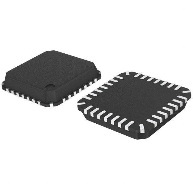
| 封装/外壳 | 8-TSSOP,8-MSOP(0.118",3.00mm 宽) |
| 工作温度 | -40°C ~ 85°C |
| 应用 | RKE,遥控系统 |
| 应用说明 | |
| 数据接口 | PCB,表面贴装 |
| 数据速率(最大值) | 50 kBaud |
| 标准包装 | 1 |
| 特性 | - |
| 电压-电源 | 2 V ~ 4 V |
| 电流-传输 | 8.5mA |
| 调制或协议 | ASK,FSK |
| 频率 | 868MHz ~ 928MHz |


- 商务部:美国ITC正式对集成电路等产品启动337调查
- 曝三星4nm工艺存在良率问题 高通将骁龙8 Gen1或转产台积电
- 太阳诱电将投资9.5亿元在常州建新厂生产MLCC 预计2023年完工
- 英特尔发布欧洲新工厂建设计划 深化IDM 2.0 战略
- 台积电先进制程称霸业界 有大客户加持明年业绩稳了
- 达到5530亿美元!SIA预计今年全球半导体销售额将创下新高
- 英特尔拟将自动驾驶子公司Mobileye上市 估值或超500亿美元
- 三星加码芯片和SET,合并消费电子和移动部门,撤换高东真等 CEO
- 三星电子宣布重大人事变动 还合并消费电子和移动部门
- 海关总署:前11个月进口集成电路产品价值2.52万亿元 增长14.8%


PDF Datasheet 数据手册内容提取
ATA8403 UHF ASK/FSK Industrial Transmitter DATASHEET Features ● Integrated PLL loop filter ● ESD protection (3kV HBM/150V MM) ● High output power (5.5dBm) with low supply current(8.5mA) ● Modulation scheme ASK/FSK ● FSK modulation is achieved by connecting an additional capacitor between the XTAL load capacitor and the open drain output of the modulating microcontroller ● Easy to design-in due to excellent isolation of the PLL from the PA and power supply ● Single Li-cell for power supply ● Supply voltage 2.0V to 4.0V in the temperature range of –40°C to +85°C ● Package TSSOP8L ● Single-ended antenna output with high efficient power amplifier ● CLK output for clocking the microcontroller ● One-chip solution with minimum external circuitry Applications ● Industrial/aftermarket remote keyless entry systems ● Alarm, telemetering, and energy metering systems ● Remote control systems for consumer and industrial markets ● Access control systems ● Home automation ● Home entertainment ● Toys 4983F-INDCO-08/15
1. Description The ATA8403 is a PLL transmitter IC, which has been developed for the demands of RF low-cost transmission systems for industrial applications at data rates up to 50kBaud ASK and 32kBaud FSK modulation scheme. The transmitting frequency range is 868MHz to 928MHz. It can be used in both FSK and ASK systems. Figure 1-1. System Block Diagram UHF ASK/FSK UHF ASK/FSK Remote control transmitter Remote control receiver 1 Li cell Atmel ATA5760/ ATA8403 ATA5761 1 to 3 Micro- Demod Control controller Encoder PLL ATARx9x Keys IF Amp Antenna Antenna XTO VCO PLL XTO LNA LNA VCO 2 ATA8403 [DATASHEET] 4983F–INDCO–08/15
2. Pin Configuration Figure 2-1. Pinning TSSOP8L ATA8403 CLK 1 8 ENABLE PA_ENABLE 2 7 GND ANT2 3 6 VS ANT1 4 5 XTAL Table 2-1. Pin Description Pin Symbol Function Configuration VS Clock output signal for 100Ω microconroller 1 CLK CLK The clock output frequency is set by the crystal to f /4 XTAL 100Ω PA_ENABLE 50kΩ U = 1.1V REF Switches on power amplifier, which 2 PA_ENABLE is used for ASK modulation 20μA ANT1 3 ANT2 Emitter of antenna output stage 4 ANT1 Open collector antenna output ANT2 ATA8403 [DATASHEET] 3 4983F–INDCO–08/15
Table 2-1. Pin Description (Continued) Pin Symbol Function Configuration VS VS 1.5kΩ 1.2kΩ 5 XTAL Connection for crystal XTAL 182μA 6 VS Supply voltage See ESD protection circuitry (see Figure 4-5 on page 8) 7 GND Ground See ESD protection circuitry (see Figure 4-5 on page 8) ENABLE 200kΩ 8 ENABLE Enable input Figure 2-2. Block Diagram Atmel ATA8403 Power up/down f CLK ENABLE 1 4 8 f 32 PA_ENABLE GND 2 PDF 7 CP ANT2 VS 3 6 LF ANT1 PA VCO XTO XTAL 4 5 PLL 4 ATA8403 [DATASHEET] 4983F–INDCO–08/15
3. General Description This fully integrated PLL transmitter allows particularly simple, low-cost RF miniature transmitters to be assembled. The VCO is locked to 64f , and therefore a 13.5672MHz crystal is needed for a 868.3MHz transmitter and a 14.2969MHz XTAL crystal for a 915MHz transmitter. All other PLL and VCO peripheral elements are integrated. The XTO is a series resonance oscillator so that only one capacitor together with a crystal connected in series to GND are needed as external elements. The crystal oscillator together with the PLL typically needs <1ms until the PLL is locked and the CLK output is stable. There is a wait time of ≥4ms must be used until the CLK is used for the microcontroller and the PA is switched on. The power amplifier is an open-collector output delivering a current pulse, which is nearly independent from the load impedance. The delivered output power is therefore controllable via the connected load impedance. This output configuration enables a simple matching to any kind of antenna or to 50. A high power efficiency of =P /(I V ) of 24% for the power amplifier at 868.3MHz results when an optimized load impedance of out S,PA S Z =(166+j226) is used at 3V supply voltage. Load 4. Functional Description If ENABLE=L and the PA_ENABLE=L, the circuit is in standby mode, consuming only a very small amount of current, so that a lithium cell used as power supply can work for several years. With ENABLE=H the XTO, PLL, and the CLK driver are switched on. If PA_ENABLE remains L, only the PLL and the XTO are running and the CLK signal is delivered to the microcontroller. The VCO locks to 64 times the XTO frequency. With ENABLE=H and PA_ENABLE=H the PLL, XTO, CLK driver, and the power amplifier are on. The power amplifier can be switched on and off with PA_ENABLE. This is used to perform the ASK modulation. 4.1 ASK Transmission The ATA8403 is activated by ENABLE=H. PA_ENABLE must remain L for t≥4ms, then the CLK signal can be taken to clock the microcontroller, and the output power can be modulated by means of the PA_ENABLE pin. After transmission, PA_ENABLE is switched to L, and the microcontroller switches back to internal clocking. The ATA8403 is switched back to standby mode with ENABLE=L. 4.2 FSK Transmission The ATA8403 is activated by ENABLE=H. PA_ENABLE must remain L for t≥4ms, then the CLK signal can be taken to clock the microcontroller and the power amplifier is switched on with PA_ENABLE=H. The chip is then ready for FSK modulation. The microcontroller starts to switch on and off the capacitor between the XTAL load capacitor and GND with an open-drain output port, thus changing the reference frequency of the PLL. If the switch is closed, the output frequency is lower than if the switch is open. After transmission PA_ENABLE is switched to L and the microcontroller switches back to internal clocking. The ATA8403 is switched back to standby mode with ENABLE=L. The accuracy of the frequency deviation with XTAL pulling method is about ±25% when the following tolerances are considered. Figure 4-1. Tolerances of Frequency Modulation VS CStray1 CStray2 LM C4 XTAL CM RS C0 C5 Crystal equivalent circuit CSwitch Using C =9.2pF±2%, C =6.8pF±5%, a switch port with C =3pF±10%, stray capacitances on each side of the crystal 4 5 Switch of C =C =1pF±10%, a parallel capacitance of the crystal of C =3.2pF±10% and a crystal with C =13fF±10%, Stray1 Stray2 0 M typically results in an FSK deviation of ±21.5kHz with worst case tolerances of ±16.8kHz to ±28.0kHz. ATA8403 [DATASHEET] 5 4983F–INDCO–08/15
4.3 CLK Output An output CLK signal is provided for a connected microcontroller. The delivered signal is CMOS compatible if the load capacitance is lower than 10pF. 4.3.1 Clock Pulse Take-over The clock of the crystal oscillator can be used for clocking the microcontroller. A special feature of Atmel®’s ATARx9x is that it starts with an integrated RC-oscillator to switch on the ATA8403 with ENABLE=H, and after 4ms assumes the clock signal of the transmission IC, so that the message can be sent with crystal accuracy. 4.3.2 Output Matching and Power Setting The output power is set by the load impedance of the antenna. The maximum output power is achieved with a load impedance of Z =(166+j226) at 868.3MHz. There must be a low resistive path to V to deliver the DC current. Load,opt S The delivered current pulse of the power amplifier is 7.7mA. The maximum output power is delivered to a resistive load of 475 if the 0.53pF output capacitance of the power amplifier is compensated by the load impedance. An optimum load impedance of: Z =475||j/(2pf0.53pF)=(166+j226) thus results in the maximum output power of 5.5dBm. Load The load impedance is defined as the impedance seen from the ATA8403’s ANT1, ANT2 into the matching network. Do not confuse this large signal load impedance with a small signal input impedance delivered as input characteristic of RF amplifiers and measured from the application into the IC instead of from the IC into the application for a power amplifier. Less output power is achieved by lowering the real parallel part of 475 where the parallel imaginary part should be kept constant. Output power measurement can be done with the circuit shown in Figure 4-2. Note that the component values must be changed to compensate for the individual board parasitics until the ATA8403 has the right load impedance Z =(166+j226) at 868.3MHz. Also the damping of the cable used to measure the output power must be calibrated Load,opt out. Figure 4-2. Output Power Measurement V S C 1 1nF L 10nH 1 Power Z = 50Ω C meter 2 ANT1 ZLopt 1.5pF Rin C 2.7pF 3 50Ω ANT2 4.4 Application Circuit A value of 68nF/X7R is recommended for the supply-voltage blocking capacitor C (see Figure 4-3 on page 7 and Figure 4- 3 4 on page 8). C and C are used to match the loop antenna to the power amplifier where C typically is 3.9pF/NP0 and C is 1 2 1 2 1pF/NP0. For C , two capacitors in series should be used to achieve a better tolerance value and to have the possibility of 2 realizing the Z using standard valued capacitors. Load,opt C , together with the pins of ATA8403 and the PCB board wires, forms a series resonance loop that suppresses the 1st 1 harmonic. Therefore, the position of C on the PCB is important. Normally the best suppression is achieved when C is 1 1 placed as close as possible to the pins ANT1 and ANT2. The loop antenna should not exceed a width of 1.5mm, otherwise the Q-factor of the loop antenna is too high. L (50nH to 100nH) can be printed on PCB. C should be selected so that the XTO runs on the load resonance frequency 1 4 of the crystal. Normally, a 15pF load-capacitance crystal results in a value of 12pF. 6 ATA8403 [DATASHEET] 4983F–INDCO–08/15
Figure 4-3. ASK Application Circuit S1 BPXY ATARx9x VDD VS 1 S2 BPXY VSS 20 BPXY OSC1 BPXY 7 Atmel ATA8403 Power up/down CLK f ENABLE 1 4 8 f 64 PA_ENABLE GND 2 PDF 7 C3 CP C2 ANT2 VS 3 6 VS Loop C1 LF Antenna ANT1 XTAL XTAL PA VCO XTO 4 5 PLL L1 C4 VS ATA8403 [DATASHEET] 7 4983F–INDCO–08/15
Figure 4-4. FSK Application Circuit S1 BPXY ATARx9x VDD VS 1 S2 BPXY VSS 20 BPXY BP42/T2O 18 OSC1 BPXY 7 Atmel ATA8403 Power up/down CLK f ENABLE 1 4 8 f 64 PA_ENABLE GND 2 PDF 7 C3 CP C2 ANT2 VS 3 6 Loop C1 LF VS Antenna C5 ANT1 XTAL XTAL PA VCO XTO 4 5 PLL L1 C4 VS Figure 4-5. ESD Protection Circuit VS ANT1 CLK PA_ENABLE ANT2 XTAL ENABLE GND 8 ATA8403 [DATASHEET] 4983F–INDCO–08/15
5. Absolute Maximum Ratings Stresses beyond those listed under “Absolute Maximum Ratings” may cause permanent damage to the device. This is a stress rating only and functional operation of the device at these or any other conditions beyond those indicated in the operational sections of this specification is not implied. Exposure to absolute maximum rating conditions for extended periods may affect device reliability. Parameters Symbol Minimum Maximum Unit Supply voltage V 5 V S Power dissipation P 100 mW tot Junction temperature T 150 °C j Storage temperature T –55 +85 °C stg Ambient temperature T –55 +85 °C amb Input voltage V –0.3 (V + 0.3)(1) V maxPA_ENABLE S Note: 1. If V + 0.3 is higher than 3.7V, the maximum voltage will be reduced to 3.7V. S 6. Thermal Resistance Parameters Symbol Value Unit Junction ambient R 170 K/W thJA 7. Electrical Characteristics V = 2.0V to 4.0V, T = 25°C unless otherwise specified. S amb Typical values are given at V = 3.0V and T = 25°C. All parameters are referred to GND (pin 7). S amb Parameters Test Conditions Symbol Min. Typ. Max. Unit Power down, V <0.25V, –40°C to 85°C 350 nA Supply current ENABLE I V <0.25V, 25°C S_Off < 10 nA PA_ENABLE (100% correlation tested) Power up, PA off, V = 3V, S I 3.6 4.6 mA V >1.7V, V <0.25V S ENABLE PA_ENABLE Supply current Power up, V =3.0, S I 8.5 11 mA V >1.7V, V >1.7V S_Transmit ENABLE PA_ENABLE V =3.0V, T =25°C, Output power S amb P 3.5 5.5 8 dBm f=868.3MHz, Z = (166 + j226) Ref Load T = 25°C, Output power variation for the full amb V = 3.0V P –1.5 dB temperature range S Ref V = 2.0V P –4.0 dB S Ref T = 25°C, amb Output power variation for the full V = 3.0V P –2.0 dB S Ref temperature range V = 2.0V, P –4.5 dB S Ref P = P + P Out Ref Ref Achievable output-power range Selectable by load impedance P –3 +5.5 dBm Out_typ f = f /128 CLK 0 Load capacitance at pin CLK = 10pF Spurious emission f ±1f –52 dBc O CLK f ±4f –52 dBc O CLK Other spurious are lower Note: 1. If V is higher than 3.6V, the maximum voltage will be reduced to 3.6V. S ATA8403 [DATASHEET] 9 4983F–INDCO–08/15
7. Electrical Characteristics (Continued) V = 2.0V to 4.0V, T = 25°C unless otherwise specified. S amb Typical values are given at V = 3.0V and T = 25°C. All parameters are referred to GND (pin 7). S amb Parameters Test Conditions Symbol Min. Typ. Max. Unit f = f /64 XTO 0 f = resonant frequency of the XTAL, Oscillator frequency XTO XTAL C ≤ 10fF, load capacitance selected f f ppm (= phase comparator frequency) M XTO XTAL accordingly T = 25°C amb PLL loop bandwidth 250 kHz Referred to f = f Phase noise of phase comparator PC XT0, –116 –110 dBc/Hz 25kHz distance to carrier In-loop phase noise PLL 25kHz distance to carrier –80 –74 dBc/Hz At 1MHz –89 –86 dBc/Hz Phase noise VCO At 36MHz –120 –117 dBc/Hz Frequency range of VCO f 868 928 MHz VCO Clock output frequency (CMOS f /256 MHz microcontroller compatible) 0 V V 0.8 V Voltage swing at pin CLK C ≤ 10pF 0h S Load V V 0.2 V 0l S Series resonance R of the crystal Rs 110 Capacitive load at pin XT0 7 pF Duty cycle of the modulation signal = FSK modulation frequency rate 0 32 kHz 50% Duty cycle of the modulation signal = ASK modulation frequency rate 0 50 kHz 50% Low level input voltage V 0.25 V Il ENABLE input High level input voltage V 1.7 V Ih Input current high I 20 µA In Low level input voltage V 0.25 V Il PA_ENABLE input High level input voltage V 1.7 V (1) V Ih S Input current high I 5 µA In Note: 1. If V is higher than 3.6V, the maximum voltage will be reduced to 3.6V. S 10 ATA8403 [DATASHEET] 4983F–INDCO–08/15
8. Ordering Information Extended Type Number Package MOQ Remarks ATA8403C-6AQY-66 TSSOP8L 5000 pcs Taped and reeled, Pb-free 9. Package Information Dimensions in mm 5 0 0515 5±0. 3±0.1 3±0.1 +0.1-0. 0.8 5 0.31+-00..0076 0.1±0.0 3.8±0.3 +0.0515-0.02 0.65 nom. 4.9±0.1 0. 3 x 0.65 = 1.95 nom. 8 5 technical drawings according to DIN specifications 1 4 03/15/04 TITLE GPC DRAWING NO. REV. Package Drawing Contact: Package: TSSOP 8L packagedrawings@atmel.com 6.543-5083.01-4 2 ATA8403 [DATASHEET] 11 4983F–INDCO–08/15
10. Revision History Please note that the following page numbers referred to in this section refer to the specific revision mentioned, not to this document. Revision No. History 4983F-INDCO-08/15 Section 8 “Ordering Information” on page 11 updated 4983E-INDCO-07/14 Put document in the latest template 4983D-INDCO-08/12 Features on page 1 changed Features on page 1 changed 4983C-INDCO-03/12 Section 8 “Ordering Information” on page 11 changed Put document in the latest template 4983B-INDCO-10/08 Section 7 “Electrical Characteristics” on page 10 changed 12 ATA8403 [DATASHEET] 4983F–INDCO–08/15
X X X X X X Atmel Corporation 1600 Technology Drive, San Jose, CA 95110 USA T: (+1)(408) 441.0311 F: (+1)(408) 436.4200 | www.atmel.com © 2015 Atmel Corporation. / Rev.: 4983F–INDCO–08/15 Atmel®, Atmel logo and combinations thereof, Enabling Unlimited Possibilities®, and others are registered trademarks or trademarks of Atmel Corporation in U.S. and other countries. Other terms and product names may be trademarks of others. DISCLAIMER: The information in this document is provided in connection with Atmel products. No license, express or implied, by estoppel or otherwise, to any intellectual property right is granted by this document or in connection with the sale of Atmel products. EXCEPT AS SET FORTH IN THE ATMEL TERMS AND CONDITIONS OF SALES LOCATED ON THE ATMEL WEBSITE, ATMEL ASSUMES NO LIABILITY WHATSOEVER AND DISCLAIMS ANY EXPRESS, IMPLIED OR STATUTORY WARRANTY RELATING TO ITS PRODUCTS INCLUDING, BUT NOT LIMITED TO, THE IMPLIED WARRANTY OF MERCHANTABILITY, FITNESS FOR A PARTICULAR PURPOSE, OR NON-INFRINGEMENT. IN NO EVENT SHALL ATMEL BE LIABLE FOR ANY DIRECT, INDIRECT, CONSEQUENTIAL, PUNITIVE, SPECIAL OR INCIDENTAL DAMAGES (INCLUDING, WITHOUT LIMITATION, DAMAGES FOR LOSS AND PROFITS, BUSINESS INTERRUPTION, OR LOSS OF INFORMATION) ARISING OUT OF THE USE OR INABILITY TO USE THIS DOCUMENT, EVEN IF ATMEL HAS BEEN ADVISED OF THE POSSIBILITY OF SUCH DAMAGES. Atmel makes no representations or warranties with respect to the accuracy or completeness of the contents of this document and reserves the right to make changes to specifications and products descriptions at any time without notice. Atmel does not make any commitment to update the information contained herein. Unless specifically provided otherwise, Atmel products are not suitable for, and shall not be used in, automotive applications. Atmel products are not intended, authorized, or warranted for use as components in applications intended to support or sustain life. SAFETY-CRITICAL, MILITARY, AND AUTOMOTIVE APPLICATIONS DISCLAIMER: Atmel products are not designed for and will not be used in connection with any applications where the failure of such products would reasonably be expected to result in significant personal injury or death (“Safety-Critical Applications”) without an Atmel officer's specific written consent. Safety-Critical Applications include, without limitation, life support devices and systems, equipment or systems for the operation of nuclear facilities and weapons systems. Atmel products are not designed nor intended for use in military or aerospace applications or environments unless specifically designated by Atmel as military-grade. Atmel products are not designed nor intended for use in automotive applications unless specifically designated by Atmel as automotive-grade.
Mouser Electronics Authorized Distributor Click to View Pricing, Inventory, Delivery & Lifecycle Information: A tmel: ATA8403C-6AQY-66