ICGOO在线商城 > 射频/IF 和 RFID > RF 发射器 > ADF7012BRUZ
 Datasheet下载
- 型号: ADF7012BRUZ
- 制造商: Analog
- 库位|库存: xxxx|xxxx
- 要求:
| 数量阶梯 | 香港交货 | 国内含税 |
| +xxxx | $xxxx | ¥xxxx |
查看当月历史价格
查看今年历史价格
ADF7012BRUZ产品简介:
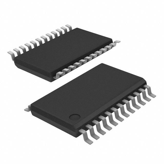
ICGOO电子元器件商城为您提供ADF7012BRUZ由Analog设计生产,在icgoo商城现货销售,并且可以通过原厂、代理商等渠道进行代购。 ADF7012BRUZ价格参考。AnalogADF7012BRUZ封装/规格:RF 发射器, RF Transmitter ASK, FSK, GFSK, OOK 75MHz ~ 1GHz -16dBm ~ 14dBm 179.2 kbps PCB, Surface Mount Antenna 24-TSSOP (0.173", 4.40mm Width)。您可以下载ADF7012BRUZ参考资料、Datasheet数据手册功能说明书,资料中有ADF7012BRUZ 详细功能的应用电路图电压和使用方法及教程。
ADF7012BRUZ 是由 Analog Devices Inc.(亚德诺半导体公司)生产的一款 RF 发射器芯片,属于 ADF70xx 系列的低功耗、高集成度无线收发器产品。其主要应用场景包括以下领域:

1. 工业无线传感器网络 (WSN):
   ADF7012BRUZ 适用于各种工业环境中的无线传感器节点,例如温度、湿度、压力或振动监测系统。它支持低功耗运行,适合电池供电的远程监控设备。

2. 智能仪表:
   在水表、电表、气表等智能仪表中,ADF7012BRUZ 可用于数据的无线传输,将消费数据发送到集中器或云端平台,实现自动化抄表和管理。

3. 家庭自动化:
   该芯片可用于智能家居系统中的无线通信模块,如门窗传感器、烟雾报警器、智能插座等设备,提供可靠的短距离无线连接。

4. 医疗健康设备:
   在便携式医疗设备中,例如心率监测仪、血糖仪或运动追踪器,ADF7012BRUZ 能够实现患者数据的实时无线传输至手机或健康管理系统。

5. 资产跟踪与物流管理:
   通过集成 GPS 或其他定位技术,ADF7012BRUZ 可以在货物运输或资产管理中实现位置信息的无线报告,提高物流效率。

6. 农业物联网 (IoT):
   在精准农业中,该芯片可应用于土壤湿度、作物生长状态或气象条件的无线监测,帮助农民优化资源利用。

7. 安全与监控系统:
   用于无线摄像头、入侵检测系统或其他安防设备的数据传输,确保信号稳定性和低延迟。

ADF7012BRUZ 支持 Sub-GHz 频段,具有低功耗特性、灵活的调制方式(如 FSK、GFSK 和 OOK)以及较高的抗干扰能力,非常适合需要长距离传输和低功耗运行的应用场景。
| 参数 | 数值 |
| 产品目录 | |
| 描述 | IC XMITTER ASK/FSK/GFSK 24TSSOP射频发射器 MultiCH ISM Band FSK /GFSK/OOK/GOOK/ASK |
| 产品分类 | |
| 品牌 | Analog Devices Inc |
| 产品手册 | |
| 产品图片 |
|
| rohs | 符合RoHS无铅 / 符合限制有害物质指令(RoHS)规范要求 |
| 产品系列 | RF集成电路,射频发射器,Analog Devices ADF7012BRUZ- |
| 数据手册 | |
| 产品型号 | ADF7012BRUZ |
| 产品培训模块 | http://www.digikey.cn/PTM/IndividualPTM.page?site=cn&lang=zhs&ptm=12876 |
| 产品目录页面 | |
| 产品种类 | 射频发射器 |
| 传输供电电流 | 16 mA |
| 功率-输出 | -16dBm ~ 14dBm |
| 包装 | 管件 |
| 商标 | Analog Devices |
| 天线连接器 | PCB,表面贴装 |
| 存储容量 | - |
| 安装风格 | SMD/SMT |
| 封装 | Tube |
| 封装/外壳 | 24-TSSOP(0.173",4.40mm 宽) |
| 封装/箱体 | TSSOP |
| 工作温度 | -40°C ~ 85°C |
| 工作电源电压 | 2.3 V to 3.6 V |
| 工作频率 | 75 MHz to 1 GHz |
| 工厂包装数量 | 62 |
| 应用 | 数据传输,RKE,遥控/安全系统 |
| 数据接口 | PCB,表面贴装 |
| 数据速率(最大值) | 179.2 kbps |
| 最大工作温度 | + 85 C |
| 最小工作温度 | - 40 C |
| 标准包装 | 62 |
| 特性 | - |
| 电压-电源 | 2.3 V ~ 3.6 V |
| 电流-传输 | 35mA |
| 电源电压-最大 | 3.6 V |
| 电源电压-最小 | 2.3 V |
| 类型 | OOK Transmitter |
| 系列 | ADF7012 |
| 视频文件 | http://www.digikey.cn/classic/video.aspx?PlayerID=1364138032001&width=640&height=505&videoID=2245193150001 |
| 调制或协议 | ASK,FSK,GFSK,OOK |
| 配用 | /product-detail/zh/EVAL-ADF7012DBZ4/EVAL-ADF7012DBZ4-ND/1530780/product-detail/zh/EVAL-ADF7012DBZ3/EVAL-ADF7012DBZ3-ND/1530779/product-detail/zh/EVAL-ADF7012DBZ2/EVAL-ADF7012DBZ2-ND/1530778/product-detail/zh/EVAL-ADF7012DBZ1/EVAL-ADF7012DBZ1-ND/1530777/product-detail/zh/EVAL-ADF7012DBZ5/EVAL-ADF7012DBZ5-ND/1523049 |
| 频率 | 75MHz ~ 1GHz |


- 商务部:美国ITC正式对集成电路等产品启动337调查
- 曝三星4nm工艺存在良率问题 高通将骁龙8 Gen1或转产台积电
- 太阳诱电将投资9.5亿元在常州建新厂生产MLCC 预计2023年完工
- 英特尔发布欧洲新工厂建设计划 深化IDM 2.0 战略
- 台积电先进制程称霸业界 有大客户加持明年业绩稳了
- 达到5530亿美元!SIA预计今年全球半导体销售额将创下新高
- 英特尔拟将自动驾驶子公司Mobileye上市 估值或超500亿美元
- 三星加码芯片和SET,合并消费电子和移动部门,撤换高东真等 CEO
- 三星电子宣布重大人事变动 还合并消费电子和移动部门
- 海关总署:前11个月进口集成电路产品价值2.52万亿元 增长14.8%


PDF Datasheet 数据手册内容提取
Multichannel ISM Band FSK/GFSK/OOK/GOOK/ASK Transmitter ADF7012 FEATURES GENERAL DESCRIPTION Single-chip, low power UHF transmitter The ADF7012 is a low power FSK/GFSK/OOK/GOOK/ASK 75 MHz to 1 GHz frequency operation UHF transmitter designed for short-range devices (SRDs). The Multichannel operation using fractional-N PLL output power, output channels, deviation frequency, and mod- 2.3 V to 3.6 V operation ulation type are programmable by using four, 32-bit registers. On-board regulator The fractional-N PLL and VCO with external inductor enable Programmable output power the user to select any frequency in the 75 MHz to 1 GHz band. −16 dBm to +14 dBm, 0.4 dB steps The fast lock times of the fractional-N PLL make the ADF7012 Data rates: dc to 179.2 kbps suitable in fast frequency hopping systems. The fine frequency Low current consumption deviations available and PLL phase noise performance facilitates 868 MHz, 10 dBm, 21 mA narrow-band operation. 433 MHz, 10 dBm, 17 mA 315 MHz, 0 dBm, 10 mA There are five selectable modulation schemes: binary frequency Programmable low battery voltage indicator shift keying (FSK), Gaussian frequency shift keying (GFSK), 24-lead TSSOP binary on-off keying (OOK), Gaussian on-off keying (GOOK), and amplitude shift keying (ASK). In the compensation register, the output can be moved in <1 ppm steps so that indirect com- APPLICATIONS pensation for frequency error in the crystal reference can be made. Low cost wireless data transfer A simple 3-wire interface controls the registers. In power-down, Security systems the part has a typical quiescent current of <0.1 μA. RF remote controls Wireless metering Secure keyless entry FUNCTIONAL BLOCK DIAGRAM PRINTED INDUCTOR OSC1 OSC2 CLKOUT L1 L2 CVCO OOK\ASK VDD ÷CLK VCO RFOUT PA DVDD ÷R CHPAFRDG/E RFGND PUMP DGND CREG LDO OOK\ASK +FRACTIONAL N REGULATOR TxCLK TxDATA FSK\GFSK Σ-Δ PLL LOCK LE DETECT MUXOUT FREQUENCY MUXOUT DATA INTSEERRFIAALCE COMCPEENNTSEARTION MBAOTNTITEORYR RSET CLK CE FREQUENCY AGND 04617-0-001 Figure 1. Rev. A Information furnished by Analog Devices is believed to be accurate and reliable. However, no responsibility is assumed by Analog Devices for its use, nor for any infringements of patents or other One Technology Way, P.O. Box 9106, Norwood, MA 02062-9106, U.S.A. rights of third parties that may result from its use. Specifications subject to change without notice. No license is granted by implication or otherwise under any patent or patent rights of Analog Devices. Tel: 781.329.4700 www.analog.com Trademarks and registered trademarks are the property of their respective owners. Fax: 781.461.3113 ©2007–2009 Analog Devices, Inc. All rights reserved.
ADF7012 TABLE OF CONTENTS Features .............................................................................................. 1 GFSK Modulation ...................................................................... 14 Applications ....................................................................................... 1 Power Amplifier ......................................................................... 14 General Description ......................................................................... 1 GOOK Modulation .................................................................... 15 Functional Block Diagram .............................................................. 1 Output Divider ........................................................................... 16 Revision History ............................................................................... 2 MUXOUT Modes....................................................................... 16 Specifications ..................................................................................... 3 Theory of Operation ...................................................................... 17 Timing Characteristics ..................................................................... 5 Choosing the External Inductor Value .................................... 17 Absolute Maximum Ratings ............................................................ 6 Choosing the Crystal/PFD Value ............................................. 17 Transistor Count ........................................................................... 6 Tips on Designing the Loop Filter ........................................... 18 ESD Caution .................................................................................. 6 PA Matching ................................................................................ 18 Pin Configuration and Function Descriptions ............................. 7 Transmit Protocol and Coding Considerations ..................... 18 Typical Performance Characteristics ............................................. 8 Application Examples .................................................................... 19 315 MHz ........................................................................................ 8 315 MHz Operation ................................................................... 20 433 MHz ........................................................................................ 9 433 MHz Operation ................................................................... 21 868 MHz ...................................................................................... 10 868 MHz Operation ................................................................... 22 Circuit Description ......................................................................... 12 915 MHz Operation ................................................................... 23 PLL Operation ............................................................................ 12 Register Descriptions ..................................................................... 24 Crystal Oscillator ........................................................................ 12 Register 0: R Register ................................................................. 24 Crystal Compensation Register ................................................ 12 Register 1: N-Counter Latch ..................................................... 25 Clock Out Circuit ....................................................................... 12 Register 2: Modulation Register ............................................... 26 Loop Filter ................................................................................... 13 Register 3: Function Register .................................................... 27 Voltage-Controlled Oscillator (VCO) ..................................... 13 Outline Dimensions ....................................................................... 28 Voltage Regulators ...................................................................... 13 Ordering Guide .......................................................................... 28 FSK Modulation .......................................................................... 13 REVISION HISTORY 6/09—Rev. 0 to Rev. A Updated Format .................................................................. Universal Changes to Table 4 ............................................................................ 7 Changes to Crystal Oscillator Section ......................................... 12 Changes to Loop Filter Section ..................................................... 13 Changes to GFSK Modulation Section ........................................ 14 Changes to Choosing the External Inductor Value Section ..... 17 Changes to Component Values—Crystal: 3.6864 MHz ............ 20 Changes to Component Values—Crystal: 4.9152 MHz ............ 21 Changes to Component Values—Crystal: 4.9152 MHz ............ 22 Changes to Component Values—Crystal: 10 MHz .................... 23 Added Register Headings Throughout ........................................ 24 Changes to Ordering Guide .......................................................... 28 10/04—Revision 0: Initial Version Rev. A | Page 2 of 28
ADF7012 SPECIFICATIONS DV = 2.3 V – 3.6 V; AGND = DGND = 0 V; T = T to T , unless otherwise noted. Operating temperature range is −40°C to +85°C. DD A MIN MAX Table 1. Parameter B Version Unit Conditions/Comments RF OUTPUT CHARACTERISTICS Operating Frequency 75/1000 MHz min/max VCO range adjustable using external inductor; divide-by-2, -4, -8 options may be required Phase Frequency Detector F /128 Hz min RF MODULATION PARAMETERS Data Rate FSK/GFSK 179.2 kbps Using 1 MHz loop bandwidth Data Rate ASK/OOK 64 Kbps Based on US FCC 15.247 specifications for ACP; higher data rates are achievable depending on local regulations Deviation FSK/GFSK PFD/214 Hz min For example, 10 MHz PFD − deviation min = ±610 Hz 511 × PFD/214 Hz max For example, 10 MHz PFD − deviation max = ±311.7 kHz GFSK BT 0.5 typ ASK Modulation Depth 25 dB max OOK Feedthrough (PA Off) −40 dBm typ F = F RF VCO −80 dBm typ F = F /2 RF VCO POWER AMPLIFIER PARAMETERS Maximum Power Setting, DV = 3.6 V 14 dBm F = 915 MHz, PA is matched into 50 Ω DD RF Maximum Power Setting, DV = 3.0 V 13.5 dBm F = 915 MHz, PA is matched into 50 Ω DD RF Maximum Power Setting, DV = 2.3 V 12.5 dBm F = 915 MHz, PA is matched into 50 Ω DD RF Maximum Power Setting, DV = 3.6 V 14.5 dBm F = 433 MHz, PA is matched into 50 Ω DD RF Maximum Power Setting, DV = 3.0 V 14 dBm F = 433 MHz, PA is matched into 50 Ω DD RF Maximum Power Setting, DV = 2.3 V 13 dBm F = 433 MHz, PA is matched into 50 Ω DD RF PA Programmability 0.4 dB typ PA output = −20 dBm to +13 dBm POWER SUPPLIES DV 2.3/3.6 V min/V max DD Current Consumption 315 MHz, 0 dBm/5 dBm 8/14 mA typ DV = 3.0 V, PA is matched into 50 Ω, I = min DD VCO 433 MHz, 0 dBm/10 dBm 10/18 mA typ 868 MHz, 0 dBm/10 dBm/14 dBm 14/21/32 mA typ 915 MHz, 0 dBm/10 dBm/14 dBm 16/24/35 mA typ VCO Current Consumption 1/8 mA min/max VCO current consumption is programmable Crystal Oscillator Current 190 μA typ Consumption Regulator Current Consumption 280 μA typ Power-Down Current 0.1/1 μA typ/max REFERENCE INPUT Crystal Reference Frequency 3.4/26 MHz min/max Single-Ended Reference Frequency 3.4/26 MHz min/max Crystal Power-On Time 3.4 MHz/26 1.8/2.2 ms typ CE to clock enable valid MHz Single-Ended Input Level CMOS levels Refer to the LOGIC INPUTS parameter. Applied OSC 2, oscillator circuit disabled. Rev. A | Page 3 of 28
ADF7012 Parameter B Version Unit Conditions/Comments PHASE-LOCKED LOOP PARAMETERS VCO Gain 315 MHz 22 MHz/V typ VCO divide-by-2 active 433 MHz 24 MHz/V typ VCO divide-by-2 active 868 MHz 80 MHz/V typ 915 MHz 88 MHz/V typ VCO Tuning Range 0.3/2.0 V min/max Spurious (IVCO Min/Max) −65/−70 dBc I is programmable VCO Charge Pump Current Setting [00] 0.3 mA typ Referring to DB[7:6] in Function Register Setting [01] 0.9 mA typ Referring to DB[7:6] in Function Register Setting [10] 1.5 mA typ Referring to DB[7:6] in Function Register Setting [11] 2.1 mA typ Referring to DB[7:6] in Function Register Phase Noise (In band)1 315 MHz −85 dBc/Hz typ PFD = 10 MHz, 5 kHz offset, I = 2 mA VCO 433 MHz −83 dBc/Hz typ PFD = 10 MHz, 5 kHz offset, I = 2 mA VCO 868 MHz −80 dBc/Hz typ PFD = 10 MHz, 5 kHz offset, I = 3 mA VCO 915 MHz −80 dBc/Hz typ PFD = 10 MHz, 5 kHz offset, I = 3 mA VCO Phase Noise (Out of Band)1 315 MHz −103 dBc/Hz typ PFD = 10 MHz, 1 MHz offset, I = 2 mA VCO 433 MHz −104 dBc/Hz typ PFD = 10 MHz, 1 MHz offset, I = 2 mA VCO 868 MHz −115 dBc/Hz typ PFD = 10 MHz, 1 MHz offset, I = 3 mA VCO 915 MHz −114 dBc/Hz typ PFD = 10 MHz, 1 MHz offset, I = 3 mA VCO Harmonic Content (Second)2 −20 dBc typ F = F RF VCO Harmonic Content (Third)2 −30 dBc typ Harmonic Content (Others)2 −27 dBc typ Harmonic Content (Second)2 −24 dBc typ F = F /N (where N = 2, 4, 8) RF VCO Harmonic Content (Third)2 −14 dBc typ Harmonic Content (Others)2 −19 dBc typ LOGIC INPUTS Input High Voltage, V 0.7 × DV V min INH DD Input Low Voltage, V 0.2 × DV V max INL DD Input Current, I /I ±1 μA max INH INL Input Capacitance, C 4.0 pF max IN LOGIC OUTPUTS Output High Voltage, V DV − 0.4 V min CMOS output chosen OH DD Output High Current, I , 500 μA max OH Output Low Voltage, V 0.4 V max I = 500 μA OL OL 1 Measurements made with NFRAC = 2048. 2 Measurements made without harmonic filter. Rev. A | Page 4 of 28
ADF7012 TIMING CHARACTERISTICS DV = 3 V ± 10%; AGND = DGND = 0 V; T = T to T , unless otherwise noted. DD A MIN MAX Table 2. Parameter Limit at T to T (B Version) Unit Test Conditions/Comments MIN MAX t 20 ns min LE setup time 1 t 10 ns min Data-to-clock setup time 2 t 10 ns min Data-to-clock hold time 3 t 25 ns min Clock high duration 4 t 25 ns min Clock low duration 5 t 10 ns min Clock-to-LE setup time 6 t 20 ns min LE pulse width 7 t t 4 5 CLK t t 2 3 DB1 DB0 (LSB) DATA DB23 (MSB) DB22 DB2 (CONTROL BIT C2) (CONTROL BIT C1) t 7 LE t1 t6 LE 04617-0-002 Figure 2. Timing Diagram Rev. A | Page 5 of 28
ADF7012 ABSOLUTE MAXIMUM RATINGS T = 25°C, unless otherwise noted. This device is a high performance RF integrated circuit with an A ESD rating of 1 kV and it is ESD sensitive. Proper precautions Table 3. should be taken for handling and assembly. Parameter Rating TRANSISTOR COUNT DV to GND −0.3 V to +3.9 V DD (GND = AGND = DGND = 0 V) 35819 (CMOS) Digital I/O Voltage to GND −0.3 V to DV + 0.3 V DD ESD CAUTION Analog I/O Voltage to GND −0.3 V to DV + 0.3 V DD Operating Temperature Range −40°C to +85°C Maximum Junction Temperature 150°C TSSOP θ Thermal Impedance 150.4°C/W JA Lead Temperature, Soldering Vapor Phase (60 sec) 215°C Infrared (15 sec) 220°C Stresses above those listed under Absolute Maximum Ratings may cause permanent damage to the device. This is a stress rating only; functional operation of the device at these or any other conditions above those listed in the operational sections of this specification is not implied. Exposure to absolute maximum rating conditions for extended periods may affect device reliability. Rev. A | Page 6 of 28
ADF7012 PIN CONFIGURATION AND FUNCTION DESCRIPTIONS DVDD 1 24 CREG2 CREG1 2 23 RSET CPOUT 3 22 AGND TxDATA 4 TSSOP 21 DVDD TxCLK 5 ADF7012 20 RFOUT MUXOUT 6 TOP VIEW 19 RFGND DGND 7 (Not to Scale) 18 VCOIN OSC1 8 17 CVCO OSC2 9 16 L2 CLKOUT 10 15 L1 DACTLAK 1112 1143 CLEE 04617-0-003 Figure 3. Pin Configuration Table 4. Pin Functional Descriptions Pin No. Mnemonic Description 1 DV Positive Supply for the Digital Circuitry. This must be between 2.3 V and 3.6 V. Decoupling capacitors to the analog ground DD plane should be placed as close as possible to this pin. 2 C A 1 μF capacitor should be added at C to reduce regulator noise and improve stability. A reduced capacitor improves REG1 REG regulator power-on time, but may cause higher spurious noise. 3 CP Charge Pump Output. This output generates current pulses that are integrated in the loop filter. The integrated current OUT changes the control voltage on the input to the VCO. 4 TxDATA Digital data to be transmitted is input on this pin. 5 TxCLK GFSK and GOOK Only. This clock output is used to synchronize microcontroller data to the TxDATA pin of the ADF7012. The clock is provided at the same frequency as the data rate. The microcontroller updates TxDATA on the falling edge of TxCLK. The rising edge of TxCLK is used to sample TxDATA at the midpoint of each bit. 6 MUXOUT Provides the Lock_Detect Signal. This signal is used to determine if the PLL is locked to the correct frequency. It also provides other signals, such as Regulator_Ready, which is an indicator of the status of the serial interface regulator, and a voltage monitor (see the MUXOUT Modes section for more information). 7 DGND Ground for Digital Section. 8 OSC1 The reference crystal should be connected between this pin and OSC2. 9 OSC2 The reference crystal should be connected between this pin and OSC1. A TCXO reference may be used, by driving this pin with CMOS levels, and powering down the crystal oscillator bit in software. 10 CLK A divided-down version of the crystal reference with output driver. The digital clock output may be used to drive several OUT other CMOS inputs, such as a microcontroller clock. The output has a 50:50 mark-space ratio. 11 CLK Serial Clock Input. This serial clock is used to clock in the serial data to the registers. The data is latched into the 32-bit shift register on the CLK rising edge. This input is a high impedance CMOS input. 12 DATA Serial Data Input. The serial data is loaded MSB first with the two LSBs being the control bits. This is a high impedance CMOS input. 13 LE Load Enable, CMOS Input. When LE goes high, the data stored in the shift registers is loaded into one of the four latches, the latch being selected using the control bits. 14 CE Chip Enable. Bringing CE low puts the ADF7012 into complete power-down, drawing < 1μA. Register values are lost when CE is low and the part must be reprogrammed once CE is brought high. 15 L1 Connected to external printed or discrete inductor. See Choosing the External Inductor Value for advice on the value of the inductor to be connected between L1 and L2. 16 L2 Connected to external printed or discrete inductor. 17 C A 22 nF capacitor should be tied between the C and C pins. This line should run underneath the ADF7012. This VCO VCO REG2 capacitor is necessary to ensure stable VCO operation. 18 VCO The tuning voltage on this pin determines the output frequency of the voltage controlled oscillator (VCO). The higher the IN tuning voltage, the higher the output frequency. 19 RF Ground for Output Stage of Transmitter. GND 20 RF The modulated signal is available at this pin. Output power levels are from –16 dBm to +12 dBm. The output should be OUT impedance matched using suitable components to the desired load. See the PA Matching section. 21 DV Voltage supply for VCO and PA section. This should have the same supply as DV (Pin 1), and should be between 2.3 V and DD DD 3.6 V. Place decoupling capacitors to the analog ground plane as close as possible to this pin. 22 AGND Ground Pin for the RF Analog Circuitry. 23 R External Resistor to set charge pump current and some internal bias currents. Use 3.6 kΩ as default. SET 24 C Add a 470 nF capacitor at C to reduce regulator noise and improve stability. A reduced capacitor improves regulator REG2 REG power-on time and phase noise, but may have stability issues over the supply and temperature. Rev. A | Page 7 of 28
ADF7012 TYPICAL PERFORMANCE CHARACTERISTICS 315 MHz –60 RBW 1MHz RF ATT 30dB = NORMAL REF LVL 0.27dBm VBW 1MHz FREQUENCY = 9.08 kHz 5dBm 308.61723447MHz SWT 17.5ms UNIT dBm –70 LEVEL =–84.47dBc/Hz 50 1 A 3 –80 –10 –20 –90 Hz) –30 2 4 1MA dBc ( –100 –40 D1–41.5dBm –110 –50 –120 –60 –70 ––1134001.0k 10.0k PHASE1 0N0O.0IkSE (Hz) 1.0M 10.004617-0-004M –––899005CEN21T [[ETT11R]]3.536M03H81..z621672–253325045..42403775ddMMBBHH7mm0zz0MH34z /[[TT11]] 9391..827692––7513521495..S4150P8125AddMGBBNHHmm7zzGHz04617-0-007 Figure 4. Phase Noise Response—DVDD = 3.0 V, ICP = 0.86 mA Figure 7. Harmonic Response, RFOUT Matched to 50 Ω, No Filter IVCO = 2.0 mA, FOUT = 315 MHz, PFD = 3.6864 MHz, PA Bias = 5.5 mA RBW 5kHz RF ATT 30dB RBW 1MHz RF ATT 30dB REF LVL 0.45dBm VBW 5kHz REF LVL 0.18dBm VBW 1MHz 5dBm 315.05060120MHz SWT 500ms UNIT dBm 5dBm 308.61723447MHz SWT 17.5ms UNIT dBm 5 5 0 1 2 A 0 1 A –10 –10 SGL –20 –20 –30 1MA –30 1MA –40 –40 3 D1–41.5dBm 2 –50 –50 4 –60 –60 –70 –70 1 [T1] 0.18dBm 3 [T1] –42.93dBm –––899005 04617-0-005 –––899005 2 [T1] 360381..621672–25532045.540375dMMBHHmzz 4 [T1] 9391..827692–75552595.450825dMGBHHmzz 04617-0-008 CENTER 315MHz 50kHz/ SPAN 500kHz CENTER 3.5MHz 700MHz/ SPAN 7GHz Figure 5. FSK Modulation, Power = 0 dBm, Data Rate = 1 kbps, Figure 8. Harmonic Response, Fifth-Order Butterworth Filter FDEVIATION = ±50 kHz RBW 500kHz RF ATT 30dB RBW 5kHz RF ATT 30dB REF LVL 0.31dBm VBW 500kHz REF LVL 20.33dBm VBW 5kHz 5dBm 315.40080160MHz SWT 5ms UNIT dBm 5dBm 26.55310621kHz SWT 500ms UNIT dBm 5 5 0 1 A 0 1 A –10 –10 –20 –20 2 3 –30 1MA –30 1MA –40 –40 D1–41.5dBm –50 D2–49dBm –50 –60 –60 –70 –70 1 [T1] –3.49dBm 315.00012525MHz 3 [T1] –20.33dB –––899005 1 [T1] 315.4008001.3610dMBHmz 04617-0-006 –––899005 2 [T1] –2267..55553511–01260022.8125kkdHHBzz 04617-0-009 CENTER 315MHz 40MHz/ SPAN 400MHz CENTER315MHz 50kHz/ SPAN500kHz Figure 6. Spurious Components—Meets FCC Specs Figure 9. OOK Modulation, Power = 0 dBm, Data Rate = 10 kbps Rev. A | Page 8 of 28
ADF7012 433 MHz 1 2.00V/ 2 1.00V/ 1.50ms500μsTRIG'D 1720mv RBW 30kHz RF ATT 40dB REF LVL 10.01dBm VBW 30kHz 15dBm 433.91158317MHz SWT 90ms UNIT dBm 15 10 1 A 0 –10 –20 1MA 2 CLKOUT –30 D1–36dBm –40 –50 –60 1 CE 04617-0-010 –––788005 04617-0-013 CENTER 433.9500601MHz 3.2MHz/ SPAN 32MHz Figure 10. Crystal Power-On Time, 4 MHz, Time = 1.6 ms Figure 13. Spurious Components—Meets ETSI Specs –40 RBW 1MHz RF ATT 40dB = NORMAL REF LVL 10.10dBm VBW 1MHz FREQUENCY = 393.38 kHz 15dBm 434.86973948MHz SWT 17.5ms UNIT dBm –60 LEVEL =–102.34dBc/Hz 1150 1 A –80 0 3 –100 –10 2 4 Hz) –20 1MA c ( –120 B –30 D1–30dBm d –140 –40 D1–36dBm –160 –50 –60 ––1280001.0k 10.0k PHASE1 0N0O.0IkSE (Hz) 1.0M 10.004617-0-011M –––788005 21 [[TT11]] 483649..876399–7411370598..12490586ddMMBBHHmmzz 43 [[TT11]] 11..370349–64–1075798..15292726ddGGBBHHmmzz 04617-0-014 CENTER 3.5GHz 700MHz/ SPAN 7GHz Figure 11. Phase Noise Response—ICP = 2.0 mA, IVCO = 2.0 mA, Figure 14. Harmonic Response, RFOUT Matched to 50 Ω, No Filter RFOUT = 433.92 MHz, PFD = 4 MHz, PA Bias = 5.5 mA RBW 10kHz RF ATT 40dB RBW 1MHz RF ATT 40dB REF LVL 5.60dBm VBW 300kHz REF LVL 9.51dBm VBW 1MHz 15dBm 433.91158317MHz SWT 44ms UNIT dBm 15dBm 434.86973948MHz SWT 17.5ms UNIT dBm 15 15 10 1 A 10 1 A 0 0 SGL –10 –10 –20 1MA –20 1MA –30 –30 2 D1–30dBm D1–36dBm D1–36dBm –40 –40 3 4 –50 –50 –60 –60 1 [T1] 9.51dBm 3 [T1] –43.60dBm –––788005 04617-0-012 –––788005 2 [T1] 483649..876399–74337398.749586dMMBHHmzz 4 [T1] 11..370349–64407398.429426dGGBHHmzz 04617-0-015 START 433.05MHz 174kHz/ STOP 434.79kHz CENTER 3.5GHz 700MHz/ SPAN 7GHz Figure 12. FSK Modulation, Power = 10 dBm, Data Rate = 38.4 kbps, Figure 15. Harmonic Response, Fifth-Order Butterworth Filter FDEVIATION = ±19.28 kHz Rev. A | Page 9 of 28
ADF7012 868 MHz 0 RBW 1MHz RF ATT 40dB = NORMAL REF LVL 12.27dBm VBW 1MHz FREQUENCY = 251.3 kHz 15dBm 869.33867735MHz SWT 16ms UNIT dBm –20 LEVEL =–99.39dBc/Hz 1150 1 A –40 0 2 –60 –10 3 4 Hz) –20 1MAX 1MA Bc ( –80 –30 D1–30dBm d –100 –40 –120 –50 –60 ––1146001.0k 10.0k PHASE1 0N0O.0IkSE (Hz) 1.0M 10.004617-0-016M –––788005CEN21T [[ETT11R]] 3.88G6H91z..373288661–752477..20337051ddMGBBHH6mm4zz0MH43z /[[TT11]] 23..549669––9111S9365P38..8092A8698NddGG BB6HHmm.4zzGHz04617-0-019 Figure 16. Phase Noise Response—ICP = 2.5 mA, IVCO = 1.44 mA, Figure 19. Harmonic Response, RFOUT Matched to 50 Ω, No Filter RFOUT = 868.95 MHz, PFD = 4.9152 MHz, Power = 12.5 dBm, PA Bias = Max RBW10kHz RF ATT 30dB RBW 1kHz RF ATT 30dB REF LVL –40.44dBm VBW10kHz MIXER –20dBm REF LVL 10.39dBm VBW 1kHz MIXER –20dBm 15dBm 869.20000000MHz SWT 15ms UNIT dBm 15dBm 869.33867735MHz SWT 10ms UNIT dBm 1150 2 A 1150 1 1 [T1] 10.39dBm A LN 869.33867735MHz LN 0 0 3 [T1] –50.92dBm 1.72000000GHz –10 –10 2 [T1] 2.596–05000.4000dGBHmz –20 1MAX 1MA –20 1MAX 1MA –30 –30 D2–30dBm D2–36dBm 1 –40 –40 2 3 –50 –50 –60 –60 1 [T1] 40.44dBm –––788005 2 [T1] 886698..2906060703803.004207dMMBHHmzz 04617-0-017 –––788005 04617-0-020 CENTER 868.944489MHz 60kHz/ SPAN 600kHz START 3.8GHz 640MHz/ SPAN 6.4GHz Figure 17. FSK Modulation, Power = 12.5 dBm, Data Rate = 38.4 kbps, Figure 20. Harmonic Response, Fifth-Order Chebyshev Filter FDEVIATION = ±19.2 kHz RBW 2kHz RF ATT 30dB REF LVL 12.55dBm VBW 2kHz MIXER –20dBm 15dBm 869.025050100MHz SWT 16s UNIT dBm 15 10 1 1 [T1] 12.55dBm A 869.02505010MHz LN 0 2 [T1] –57.89dBm 859.16695500MHz –10 3 [T1] 862.000–08010.9070dMBHmz –20 1MAX 1MA –30 D2–36dBm –40 –50 2 D1–54dBm –60 –––788005 3 04617-0-018 START 856.5MHz 2.5MHz/ STOP 881.5MHz Figure 18. Spurious Components—Meets ETSI Specs Rev. A | Page 10 of 28
ADF7012 915 MHz –40 = NORMAL R15EdFB LmVL 907.81561301.2256dMBHmz RVSBWBWWT 5500MM6.HH4szz RUFN IATTT 4d0BdmB FREQUENCY = 992.38 kHz 15 –60 LEVEL =–102.34dBc/Hz 10 1 A –80 0 2 –10 –100 4 Hz) –20 1MAX 3 1MA c ( –120 B –30 d –140 –40 D1–41.5dBm –160 –50 ––1280001.0k 10.0k PHASE1 0N0O.0IkSE (Hz) 1.0M 10.004617-0-021M ––––67880005 21 [[TT11]] 9071..881351–6211360012..02256563ddMGBBHHmmzz 34 [[TT11]] 23..764512––8521800735..25709071ddGGBBHHmmzz 04617-0-038 CENTER 3.8GHz 640MHz/ SPAN 6.4GHz Figure 21. Phase Noise Response—ICP = 1.44 mA, IVCO = 3.0 mA, Figure 24. Harmonic Response, RFOUT Matched to 50 Ω, No Filter RFOUT = 915.2 MHz, PFD =10 MHz, Power = 10 dBm, PA Bias = 5.5 mA RBW 10kHz RF ATT 40dB RBW 50MHz RF ATT 40dB REF LVL 3.88dBm VBW300kHz REF LVL 9.06dBm VBW 50MHz 15dBm 915.19098196MHz SWT 15ms UNIT dBm 15dBm 907.81563126MHz SWT 6.4s UNIT dBm 15 15 10 1 A 10 1 A 0 0 –10 –10 –20 1MAX 1MA –20 1MAX 1MA –30 –30 –40 –40 2 3 4 D1–41.5dBm –50 –50 –60 –60 1 [T1] 9.06dBm 3 [T1] –46.22dBm –––788005 04617-0-036 –––788005 2 [T1] 9071..881351–62436812.425063dMGBHHmzz 4 [T1] 23..764512–85480635.970671dGGBHHmzz 04617-0-039 CENTER 915.190982MHz 50kHz/ SPAN 500kHz CENTER 3.8GHz 640MHz/ SPAN 6.4GHz Figure 22. FSK Modulation, Power = 10 dBm, Data Rate = 38.4 kbps, Figure 25. Harmonic Response, Fifth-Order Chebyshev Filter FDEVIATION = ±19.2 kHz RBW 10kHz RF ATT 40dB REF LVL 9.94dBm VBW300kHz 15dBm 915.23167977MHz SWT 100ms UNIT dBm 15 1 * 10 A 0 SGL –10 –20 1MA –30 –40 D1–41.5dBm D1–49.5dBm –50 –60 –––788005 04617-0-037 CENTER 915.2MHz 40MHz/ SPAN 400MHz Figure 23. Spurious Components—Meets FCC Specs Rev. A | Page 11 of 28
ADF7012 CIRCUIT DESCRIPTION PLL OPERATION OSC1 OSC2 Agsiem nfreparlcyatt ibeodyn cafrhl-oaNmn gP aiLn sLgin taghllleeo -wprreso fmegrrueanlmtcipmel oea sbocluielt lNpaut ovtr af rl(ueueqs uufoeaunllnyci dae sic ntro yt hsbteea l ) CP2 CP1 04617-0-023 Figure 27. Oscillator Circuit on the ADF7012 N register. At the phase frequency detector (PFD), the reference Two parallel resonant capacitors are required for oscillation at is compared to a divided-down version of the output frequency the correct frequency—the value of these depend on the crystal (VCO/N). If VCO/N is too low a frequency, typically the output specification. They should be chosen so that the series value of frequency is lower than desired, and the PFD and charge-pump capacitance added to the PCB track capacitance adds to give the combination sends additional current pulses to the loop filter. load capacitance of the crystal, usually 20 pF. Track capacitance This increases the voltage applied to the input of the VCO. values vary between 2 pF to 5 pF, depending on board layout. Because the VCO of the ADF7012 has a positive frequency vs. voltage characteristic, any increase in the VTUNE voltage applied Where possible, to ensure stable frequency operation over all to the VCO input increases the output frequency at a rate of conditions, capacitors should be chosen so that they have a kilovolts, the tuning sensitivity of the VCO (MHz/V). At each very low temperature coefficient and/or opposite temperature interval of 1/PFD seconds, a comparison is made at the PFD coefficients until the PFD and charge pump eventually force a state of Typically, for a 10 MHz crystal with 20 pF load capacitance, equilibrium in the PLL where PFD frequency = VCO/N. At the oscillator circuit can tolerate a crystal ESR value of ≤ 50 Ω. this point, the PLL can be described as locked. The ESR tolerance of the ADF7012 decreases as crystal fre- CRYSTAL/R quency increases, but this can be offset by using a crystal with LOOP FILTER lower load capacitance. R PFD CP CRYSTAL COMPENSATION REGISTER FVCO VCO The ADF7012 features a 15-bit fixed modulus, which allows the VCO/N N 04617-0-022 orteeumstoppluuettr iafortneuq rceua ednnr bcifyet utinos ebtdhe e ta ord eejfuaessrtieelynd cc ieon cm srtpyeseptnass lo.a ft eF fPoFrD in/i1t5ia. lT ehrriso rfi nane d Figure 26. Fractional-N PLL F = F × FEC (3) ADJUST STEP where: F ×N F = CRYSTAL =F ×N (1) F = FPFD/215 OUT R PFD STEP FEC = Bit F1 to Bit F11 in the R Register For a fractional-N PLL Note that the notation is twos complement, so F11 represents ⎛ N ⎞ the sign of the FEC number. F =F ×⎜N + FRAC ⎟ (2) OUT PFD ⎝ INT 212 ⎠ Example F = 10 MHz where N can be Bits M1 to M12 in the fractional-N register. PFD FRAC F = −11 kHz ADJUST CRYSTAL OSCILLATOR F = 10 MHz/215 = 305.176 Hz STEP The on-board crystal oscillator circuitry (Figure 27) allows an FEC = −11 kHz/305.17 Hz = −36 = −(00000100100) = inexpensive quartz crystal to be used as the PLL reference. The 11111011100 = 0x7DC oscillator circuit is enabled by setting XOEB low. It is enabled by CLOCK OUT CIRCUIT default on power-up and is disabled by bringing CE low. Errors The clock out circuit takes the reference clock signal from the in the crystal can be corrected using the error correction Crystal Oscillator section and supplies a divided-down 50:50 register within the R register. mark-space signal to the CLK pin. An even divide from OUT A single-ended reference may be used instead of a crystal, by 2 to 30 is available. This divide is set by the DB[19:22] in the applying a square wave to the OSC2 pin, with XOEB set high. R register. On power-up, the CLK defaults to divide by 16. OUT Rev. A | Page 12 of 28
ADF7012 DVDD The varactor capacitance can be adjusted in software to increase CLKOUT the effective VCO range by writing to the VA1 and VA2 bits in ENABLE BIT the R register. Under typical conditions, setting VA1 and VA2 high increases the center frequency by reducing the varactor OSC1 D1I VTIOD E15R ÷2 CLKOUT 04617-0-024 cFaigpuarceit 3an7 cseh boyw as pthpreo vxairmiaattieolny o1f.3 V pCFO. gain with frequency. Figure 28. CLKOUT Stage VCO gain is important in determining the loop filter design— The output buffer to CLK is enabled by setting Bit DB4 in predictable changes in VCO gain resulting in a change in the OUT the function register high. On power-up, this bit is set high. loop filter bandwidth can be offset by changing the charge- The output buffer can drive up to a 20 pF load with a 10% rise pump current in software. time at 4.8 MHz. Faster edges can result in some spurious VCO Bias Current feedthrough to the output. A small series resistor (50 Ω) can VCO bias current may be adjusted using bits VB1 to VB4 in the be used to slow the clock edges to reduce these spurs at F . CLK function register. Additional bias current will reduce spurious LOOP FILTER levels, but increase overall current consumption in the part. A The loop filter integrates the current pulses from the charge bias value of 0x5 should ensure oscillation at most frequencies pump to form a voltage that tunes the output of the VCO to the and supplies. Settings 0x0, 0xE , and 0xF are not recommended. desired frequency. It also attenuates spurious levels generated by Setting 0x3 and Setting 0x4 are recommended under most the PLL. A typical loop filter design is shown in Figure 29. conditions. Improved phase noise can be achieved for lower bias currents. VOLTAGE REGULATORS CHARGE VCO PUMP OUT There are two band gap voltage regulators on the ADF7012 04617-0-025 p(Xro5vRid, NinPg0 a) sttoa bglreo u2.n2d5 aVt CinRtEeGr1n aanl ds uap 4p7ly0: naF 2 c.2a pμaFc citaopra acti tCoRrE G2 Figure 29. Typical Loop Filter should be used to ensure stability. The internal reference In FSK, it is recommended that the loop bandwidth be a ensures consistent performance over all supplies and reduces minimum of two to three times the data rate. Widening the the current consumption of each of the blocks. LBW excessively reduces the time spent jumping between The combination of regulators, band gap reference, and biasing frequencies, but results in reduced spurious attenuation. See typically consume 1.045 mA at 3.0 V and can be powered down the Tips on Designing the Loop Filter section. by bringing the CE line low. The serial interface is supplied by For OOK/ASK systems, a wider loop bandwidth than for FSK Regulator 1, so powering down the CE line causes the contents systems is desirable. The sudden large transition between two of the registers to be lost. The CE line must be high and the reg- power levels results in VCO pulling (VCO temporarily goes to ulators must be fully powered on to write to the serial interface. incorrect frequency) and can cause a wider output spectrum. Regulator power-on time is typically 100 μs and should be taken By widening the loop bandwidth a minimum of 10× the data into account when writing to the ADF7012 after power-up. rate, VCO pulling is minimized because the loop settles quickly Alternatively, regulator status may be monitored at the MUXOUT back to the correct frequency. A free design tool, the ADI SRD pin once CE has been asserted, because MUXOUT defaults to Design Studio™, can be used to design loop filters for the Analog the regulator ready signal. Once Regulator_ready is high, the Devices family of transmitters. regulator is powered up and the serial interface is active. VOLTAGE-CONTROLLED OSCILLATOR (VCO) FSK MODULATION The ADF7012 features an on-chip VCO with an external tank FSK modulation is performed internally in the PLL loop by inductor, which is used to set the frequency range. The center switching the value of the N register based on the status of frequency of oscillation is governed by the internal varactor the TxDATA line. The TxDATA line is sampled at each cycle capacitance and that of the external inductor combined with of the PFD block (every 1/FPFD seconds). When TxDATA the bond-wire inductance. An approximation for this is given makes a low-to-high transition, an N value representing the in Equation 4. For a more accurate selection of the inductor, deviation frequency is added to the N value representing the see the section Choosing the External Inductor Value. center frequency. Immediately the loop begins to lock to the new frequency of F + F . Conversely, when TxDATA CENTER DEVIATION 1 F = (4) makes a high-to-low transition, the N value representing the VCO 2π (LINT+LEXT)×(CVAR+CFIXED) deviation is subtracted from the PLL N value representing the center frequency and the loop transitions to F − F . CENTER DEVIATION Rev. A | Page 13 of 28
ADF7012 For GFSK and GOOK, the incoming bit stream to be trans- mitted needs to be synchronized with an on-chip sampling clock which provides one sample per bit to the Gaussian FIR filter. To facilitate this, the sampling clock is routed to the 4R PFD/ PA STAGE CHARGE VCO TxCLK pin where data is fetched from the host microcontroller PUMP or microprocessor on the falling edge of TxCLK, and the data FSK DEVIATION is sampled at the midpoint of each bit on TxCLK’s rising edge. FREQUENCY ÷N Inserting external RC LPFs on TxDATA and TxCLK lines creates smoother edge transitions and improves spurious –FDEV THIRD-ORDER performance. As an example, suitable components are a 1 kΩ Tx+DFADTEAV FRACTIONAL-NΣ-Δ MODULATOR INTEGER-N 04617-0-026 resistor and a 10 nF capacitor for a data rate of 5 kbps. Figure 30. FSK Implementation I/O TxDATA μC ADF7012 TDh9e b ditesv iina ttihoen mfroomdu tlahtei ocne nrteegri sftreerq. uTehnec yfr eisq sueetn ucsyi ndge vthiaet iDon1 to INT FETCH FETCH FETCH FETCH TxCLK 04617-0-040 may be set in steps of SAMPLE SAMPLE SAMPLE F Figure 31. TxCLK/TxDATA Synchronization. F (Hz)= PFD (5) STEP 214 The number of steps between symbol 0 and symbol 1 is The deviation frequency is therefore determined by the setting for the index counter. The GFSK deviation is set up as F ×ModulationNumber F (Hz)= PFD (6) DEVIATION 214 F ×2m GFSK (Hz)= PFD (7) where ModulationNumber is set by Bit D1 to Bit D9. DEVIATION 212 The maximum data rate is a function of the PLL lock time (and where m is the mod control (Bit MC1 to Bit MC3 in the the requirement on FSK spectrum). Because the PLL lock time modulation register). is reduced by increasing the loop-filter bandwidth, highest data The GFSK sampling clock samples data at the data rate rates can be achieved for the wider loop filter bandwidths. The F absolute maximum limit on loop filter bandwidth to ensure DataRate(bps)= PFD (8) DividerFactor×IndexCounter stability for a fractional-N PLL is F /7. For a 20 MHz PFD PFD frequency, the loop bandwidth could be as high as 2.85 MHz. where the DividerFactor is set by Bit D1 to Bit D7, and the FSK modulation is selected by setting the S1 and S2 bits in the IndexCounter is set by Bit IC1 and Bit IC2 in the modulation modulation register low. register. GFSK MODULATION POWER AMPLIFIER Gaussian frequency shift keying (GFSK) represents a filtered The output stage is based on a Class E amplifier design, with form of frequency shift keying. The data to be modulated to an open-drain output switched by the VCO signal. The output RF is prefiltered digitally using a finite impulse response filter control consists of six current mirrors operating as a program- (FIR). The filtered data is then used to modulate the sigma- mable current source. delta fractional-N to generate spectrally-efficient FSK. To achieve maximum voltage swing, the RF pin needs to be OUT FSK consists of a series of sharp transitions in frequency as the biased at DV . A single pull-up inductor to DV ensures a DD DD data is switched from one level to another. The sharp switching current supply to the output stage; PA is biased to DV volts, DD generates higher frequency components at the output, resulting and with the correct choice of value transforms the impedance. in a wider output spectrum. The output power can be adjusted by changing the value of With GFSK, the sharp transitions are replaced with up to 128 Bit P1 to Bit P6. Typically, this is P1 to P6 output −20dBm at smaller steps. The result is a gradual change in frequency. As a 0x0, and 13 dBm at 0x7E at 868 MHz, with the optimum result, the higher frequency components are reduced and the matching network. spectrum occupied is reduced significantly. GFSK does require some additional design work as the data is only sampled once per bit, and so the choice of crystal is important to ensure the correct sampling clock is generated. Rev. A | Page 14 of 28
ADF7012 The nonlinear characteristic of the output stage results in an As is the case with GFSK, GOOK requires the bit stream output spectrum containing harmonics of the fundamental, applied at TxDATA to be synchronized with the sampling clock, especially the third and fifth. To meet local regulations, a low- TxCLK (see the GFSK Modulation section). pass filter usually is required to filter these harmonics. The output stage can be powered down by setting Bit PD2 in 10 the function register low. 0 GOOK MODULATION –10 Gaussian on-off keying (GOOK) represents a prefiltered form OOK –20 of OOK modulation. The usually sharp symbol transitions m) B are replaced with smooth Gaussian-filtered transitions with d –30 R ( the result being a reduction in frequency pulling of the VCO. WE –40 Frequency pulling of the VCO in OOK mode can lead to a PO –50 wider than desired bandwidth, especially if it is not possible to increase the loop filter bandwidth to > 300 kHz. –60 The GOOK sampling clock samplesF data at the data rate: ––7890009.43 GOOK 910.43 910.904617-0-0433 DataRate(bps)= PFD (9) DividerFactor×IndexCounter FREQUENCY (MHz) Figure 33. GOOK vs. OOK Frequency Spectra Bit D1 to Bit D6 represent the output power for the system (Narrow-Band Measurement) for a positive data bit. Divider Factor = 0x3F represents the maximum possible deviation from PA at minimum to PA 20 at maximum output. Note that PA output level bits in Register 2 10 are defunct. An index counter setting of 128 is recommended. 0 Figure 32 shows the step response of the Gaussian FIR filter. –10 An index counter of 16 is demonstrated for simplicity. While m) –20 twhieth p rae l-ofwilt-etro -dhaitgah w doautlad t rsawnitscithio tnh,e t PhAe fdilitreercetdly d fartoam g roafdf utoa lolyn WER (dB ––3400 OOK increases the PA output in discrete steps. This has the effect of O P –50 making the output spectrum more compact. –60 PRE-FILTER DATA –70 1P6A ( SMEATXT)ING (0 TO 1 TRANSITION) ––9800 GOOK 04617-0-044 15 885.43 910.43 935.93 14 FREQUENCY (MHz) 13 12 Figure 34. GOOK vs. OOK Frequency Spectra 11 (Wideband Measurement) 10 9 8 7 6 5 DISCRETIZED 4 FILTER OUTPUT 132 (PA OFF) 04617-0-041 Figure 32. Varying PA Output for GOOK (Index Counter = 16). Rev. A | Page 15 of 28
ADF7012 OUTPUT DIVIDER Battery Voltage Readback An output divider is a programmable divider following the By setting MUXOUT to 1010 to 1101, the battery voltage can VCO in the PLL loop. It is useful when using the ADF7012 to be estimated. The battery measuring circuit features a voltage generate frequencies of < 500 MHz. divider and a comparator where the divided-down supply voltage is compared to the regulator voltage. REFERENCE LOOP OUTPUT DIVIDER PFD CP FILTER VCO DIVIDER PA Table 6. ÷N ÷1/2/4/8 04617-0-042 M10U1X0 OUT MDVUDXD O<U 2T.3 H5 iVg h MDVUDXD O>U 2T.3 L5o Vw Figure 35. Output Divider Location in PLL 1011 DV < 2.75 V DV > 2.75 V DD DD The output divider may be used to reduce feedthrough of the 1100 DVDD < 3.0 V DVDD > 3.0 V VCO by amplifying only the VCO/2 component, restricting the 1101 DVDD < 3.25 V DVDD > 3.25 V VCO feedthrough to leakage. The accuracy of the measurement is limited by the accuracy of Because the divider is in loop, the N register values should be the regulator voltage and the internal resistor tolerances. set up according to the usual formula. However, the VCO gain Regulator Ready (K ) should be scaled according to the divider setting, as shown V The regulator has a power-up time, dependant on process and in the following example: the external capacitor. The regulator ready signal indicates that F = 433 MHz OUT the regulator is fully powered, and that the serial interface is F = 866 MHz VCO active. This is the default setting on power-up at MUXOUT. K @ 868 MHz = 60 MHz/V V Digital Lock Detect Therefore, K for loop filter design = 30 MHz/V. V Digital lock detect indicates that the status of the PLL loop. The divider value is set in the R register. The PLL loop takes time to settle on power-up and when the frequency of the loop is changed by changing the N value. Table 5. When lock detect is high, the PFD has counted a number of OD1 OD2 Divider Status consecutive cycles where the phase error is < 15 ns. The lock 0 0 Divider off detect precision bit in the function register determines whether 0 1 Divide by 2 this is three cycles (LDP = 0), or five cycles (LDP = 1). It is 1 0 Divide by 4 recommended that LDP be set to 1. The lock detect is not 1 1 Divide by 8 completely accurate and goes high before the output has settled to exactly the correct frequency. In general, add 50% to the MUXOUT MODES indicated lock time to obtain lock time to within 1 kHz. The The MUXOUT pin allows the user access to various internal lock detect signal can be used to decide when the power signals in the transmitter, and provides information on the amplifier (PA) should be enabled. PLL lock status, the regulator, and the battery voltage. The R Divider MUXOUT is accessed by programming Bits M1 to M4 in the MUXOUT provides the output of the R divider. This is a function register and observing the signal at the MUXOUT pin. narrow pulsed digital signal at frequency F . This signal PFD may be used to check the operation of the crystal circuit and the R divider. R divider/2 is a buffered version of this signal at F /2. PFD Rev. A | Page 16 of 28
ADF7012 THEORY OF OPERATION CHOOSING THE EXTERNAL INDUCTOR VALUE CHOOSING THE CRYSTAL/PFD VALUE The ADF7012 allows operation at many different frequencies by The choice of crystal value is an important one. The PFD choosing the external VCO inductor to give the correct output frequency must be the same as the crystal value or an integer frequency. Figure 36 shows both the minimum and maximum division of it. The PFD determines the phase noise, spurious frequency vs. the inductor value. These are measurements based levels and location, deviation frequency, and the data rate in on 0603 CS type inductors from Coilcraft, and are intended as the case of GFSK. The following sections describe some factors guidelines in choosing the inductor because board layout and to consider when choosing the crystal value. inductor type varies between applications. Standard Crystal Values The inductor value should be chosen so that the VCO is cen- Standard crystal values are 3.6864 MHz, 4 MHz, 4.096 MHz, tered at the correct frequency. When locked, the VCO tuning 4.9152 MHz, 7.3728 MHz, 9.8304 MHz, 10 MHz, 11.0592 MHz, voltage can be between 0.2 V and 2.1 V. This voltage can be 12 MHz, and 14.4792 MHz. Crystals with these values are measured at Pin 18 (VCO ). To ensure operation over IN usually available in stock and cost less than crystals with temperature and from part to part, an inductor should be nonstandard values. chosen so that the tuning voltage is ~1 V at the desired output Reference Spurious Levels frequency. Reference spurious levels (spurs) occur at multiples of the 1200 MIN(meas) PFD frequency. The reference spur closest to the carrier is 1100 MAX(meas) usually highest with the spur further out being attenuated by 1000 MIN(eqn) the loop filter. The level of reference spur is lower for lower MAX(eqn) PFD frequencies. In designs with high output power where Hz) 900 M spurious levels are the main concern, a lower PFD frequency CY ( 800 (<5 MHz) may be desirable. N UE 700 Beat Note Spurs Q E FR 600 Beat note spurs are spurs occurring for very small or very large 500 values in the fractional register. These are quickly attenuated by 4300000 5 10 15 20 25 30 3504617-0-031 tltorhacena ltsoimoonpit, t feailrnt edsrp .e eSncestlureurcemtsio .t nh aotf t thheey PhFaDve tnheegrelifgoirbel ed eeftfeercmt ionne sth teh eir INDUCTANCE (nH) Phase Noise Figure 36. Output Frequency vs. External Inductor Value IBIAS = 2.0 mA. The phase noise of a frequency synthesizer improves by 3 dB For frequencies between 270 MHz and 550 MHz, it is recom- for every doubling of the PFD frequency. Because ACP is mended to operate the VCO at twice the desired output related to the phase noise, the PFD may be increased to reduce frequency and use the divide-by-2 option. This ensures reliable the ACP in the system. PFD frequencies of < 5 MHz typically operation over temperature and supply. deliver sufficient phase noise performance for most systems. For frequencies between 130 MHz and 270 MHz, it is recom- Deviation Frequency mended to operate the VCO at four times the desired output The deviation frequency is adjustable in steps of frequency and use the divide-by-4 option. F F (Hz)= PFD (10) For frequencies below 130 MHz, it is best to use the divide- STEP 214 by-8 option. It is not necessary to use the VCO divider for To get the exact deviation frequency required, ensure F is a frequencies above 550 MHz. STEP factor of the desired deviation. ADIsimSRD Design Studio is a design tool which can perform the frequency calculations for the ADF7012, and is available at www.analog.com. Rev. A | Page 17 of 28
ADF7012 TIPS ON DESIGNING THE LOOP FILTER Spurious Levels In the case where the output power is quite high, a reduced loop The loop filter design is crucial in ensuring stable operation filter bandwidth reduces the spurious levels even further, and of the transmitter, meeting adjacent channel power (ACP) provides additional margin on the specification. specifications, and meeting spurious requirements for the relevant regulations. ADIsimSRD Design Studio™ is a free tool The following sections provide examples of loop filter designs available to aid the design of loop filters. The user enters the for typical applications in specific frequencies. desired frequency range, the reference crystal and PFD values, PA MATCHING and the desired loop bandwidth. ADIsimSRD Design Studio The ADF7012 exhibits optimum performance in terms of gives a good starting point for the filter, and the filter can be transmit power and current consumption only if the RF output further optimized based on the criteria below. port is properly matched to the antenna impedance. Setting Tuning Sensitivity Value ZOPT_PA depends primarily on the required output power, The tuning sensitivity or kV, usually denoted in MHz/V, is and the frequency range. Selecting the optimum ZOPT_PA required for the loop filter design. It refers to the amount that helps to minimize the current consumption. This data sheet a change of a volt in the voltage applied to the VCOIN pin, contains a number of matching networks for common fre- changes the output frequency. Typical data for the ADF7012 quency bands. Under certain conditions it is recommended over a frequency range is shown. to obtain a suitable ZOPT_PA value by means of a load-pull 120 measurement. 100 DVDD 80 V) RFOUT MHz/ 60 ANTENNA LPF PA (V K 40 ZOPT_PA 04617-0-033 Figure 38. ADF7012 with Harmonic Filter 200 004617-0-032 Tarhee f oimr 5p0e dΩa necnev miroantcmheinngts v. aAlune as dpdriotvioidneadl mina ttchhei nnegx nt estewctoirokn 200 300 400 500 600 700 800 900 1000 1100 FREQUENCY (MHz) may be required after the harmonic filter to match to the Figure 37. kV vs. VCO Frequency antenna impedance. This can be incorporated into the filter design itself in order to reduce external components. Charge-Pump Current TRANSMIT PROTOCOL AND CODING The charge-pump current allows the loop filter bandwidth to be CONSIDERATIONS changed using the registers. The loop bandwidth reduces as the charge pump current is reduced and vice versa. Selecting Loop Filter Bandwidth PREAMBLE WSYONRCD FIEIDLD DATA FIELD CRC 04617-0-034 Data Rate Figure 39. Typical Format of a Transmit Protocol The loop filter bandwidth should usually be at two to three A dc-free preamble pattern such as 10101010… is recom- times the data rate. This ensures that the PLL has ample time mended for FSK/ASK/OOK demodulation. Preamble patterns to jump between the mark and space frequencies. with longer run-length constraints such as 11001100…. can also ACP be used. However, this can result in a longer synchronization In the case where the ACP specifications are difficult to meet, time of the received bit stream in the chosen receiver. the loop filter bandwidth can be reduced further to reduce the phase noise at the adjacent channel. The filter rolls off at 20 dB per decade. Rev. A | Page 18 of 28
ADF7012 APPLICATION EXAMPLES 530-0-71640 Figure 40. Applications Diagram with Harmonic Filter Rev. A | Page 19 of 28
ADF7012 315 MHz OPERATION Deviation The recommendations presented here are guidelines only. The deviation is set to ± 50 kHz to accommodate simple The design should be subject to internal testing prior to FCC receiver architecture. site testing. Matching components need to be adjusted for The modulation steps available are in 3.6864 MHz/214 : board layout. Modulation steps = 225 Hz The FCC standard 15.231 regulates operation in the band Modulation number = 50 kHz/225 Hz = 222 from 260 MHz to 470 MHz in the US. This is used generally Bias Current in the transmission of RF control signals, such as in a satellite- Because low current is desired, a 2.0 mA VCO bias can be used. decoder remote control, or remote keyless entry system. Additional bias current reduces any spur, but increases current The band cannot be used to send any continuous signal. The consumption. maximum output power allowed is governed by the duty cycle of the system. A typical design example for a remote control The PA bias can be set to 5.5 mA and can achieve 0 dBm. is provided. Loop Filter Bandwidth Design Criteria The loop filter is designed with the ADIsimSRD Design Studio. 315 MHz center frequency The loop bandwidth design is straightforward because the FSK/OOK modulation 20 dB bandwidth is generally of the order of >400 kHz (0.25% 1 mW output power of center frequency). A loop bandwidth of close to 100 kHz House range strikes a good balance between lock time and spurious Meets FCC 15.231 suppression. If it is found that pulling of the VCO is more than desired in OOK mode, the bandwidth could be increased. The main requirements in the design of this remote are a long battery life and sufficient range. It is possible to adjust the Design of Harmonic Filter output power of the ADF7012 to increase the range depending The main requirement of the harmonic filter should ensure on the antenna performance. that the third harmonic level is < −41.5 dBm. A fifth-order The center frequency is 315 MHz. Because the ADF7012 Chebyshev filter is recommended to achieve this, and a VCO is not recommended for operation in fundamental mode suggested starting point is given next. The Pi format is chosen for frequencies below 400 MHz, the VCO needs to operate at to minimize the more expensive inductors. 630 MHz. Figure 36 implies an inductor value of, or close to, Component Values—Crystal: 3.6864 MHz 7.6 nH. The chip inductor chosen = 7.5 nH (0402CS-7N5 Loop Filter from Coilcraft). Coil inductors are recommended to provide I 0.866 mA CP sufficient Q for oscillation. LBW 100 kHz Crystal and PFD C1 680 pF Phase noise requirements are not excessive as the adjacent C2 12 nF channel power requirement is −20 dB. The PFD is chosen to C3 220 pF minimize spurious levels (beat note and reference), and to R1 1.1 kΩ ensure a quick crystal power-up time. R2 3 kΩ PFD = 3.6864 MHz − power-up time 1.6 ms. Matching L1 56 nH Figure 10 shows a typical power-on time for a 4 MHz crystal. L2 1 nF N-Divider C14 470 pF The N-divider is determined as being Harmonic Filter NINT = 85 L4 22 nH NFRAC = (1850)/4096 L5 22 nH VCO divide-by-2 is enabled C15 3.3 pF C16 8.2 pF C17 3.3 pF Rev. A | Page 20 of 28
ADF7012 433 MHz OPERATION Bias Current The recommendations here are guidelines only. The design should be subject to internal testing prior to ETSI site testing. Because low current is desired, a 2.0 mA VCO bias can be used. Matching components need to be adjusted for board layout. Additional bias current reduces any spurious, but increases current consumption. The ETSI standard EN 300-220 governs operation in the 433.050 MHz to 434.790 MHz band. For many systems, 10% The PA bias can be set to 5.5 mA and achieve 10 dBm. duty is sufficient for the transmitter to output 10 dBm. Loop Filter Bandwidth Design Criteria The loop filter is designed with ADIsimSRD Design Studio. 433.92 MHz center frequency The loop bandwidth design requires that the channel power FSK modulation be < −36 dBm at ±870 kHz from the center. A loop bandwidth 10 mW output power of close to 160 kHz strikes a good balance between lock time for 200 m range data rates, including 32 kbps and spurious suppression. If it is Meets ETSI 300-220 found that pulling of the VCO is more than desired in OOK mode, the bandwidth could be increased. The main requirement in the design of this remote is a long battery life and sufficient range. It is possible to adjust the Design of Harmonic Filter output power of the ADF7012 to increase the range depending The main requirement of the harmonic filter should ensure on the antenna performance. that the third harmonic level is < −30 dBm. A fifth-order The center frequency is 433.92 MHz. It is possible to operate the Chebyshev filter is recommended to achieve this, and a VCO at this frequency. Figure 36 shows the inductor value vs. suggested starting point is given next. The Pi format is chosen center frequency. The inductor chosen is 22 nH. Coilcraft to minimize the more expensive inductors. inductors such as 0603-CS-22NXJBU are recommended. Component Values—Crystal: 4.9152 MHz Crystal and PFD Loop Filter The phase noise requirement is such to ensure the power at Icp 2.0 mA the edge of the band is < −36 dBm. The PFD is chosen to LBW 100 kHz minimize spurious levels (beat note and reference), and to C1 680 pF ensure a quick crystal power-up time. C2 12 nF C3 270 pF PFD = 4.9152 MHz − Power-Up Time 1.6 ms. Figure 10 shows a R1 910 Ω typical power-up time for a 4 MHz crystal. R2 3.3 kΩ N-Divider Matching The N Divider is determined as being: L1 22 nH Nint = 88 L2 10 pF Nfrac = (1152)/4096 C14 470 pF VCO divide-by-2 is not enabled Deviation Harmonic Filter The deviation is set to ± 50 kHz to accommodate a simple L4 22 nH receiver architecture. L5 22 nH C15 3.3 pF The modulation steps available are in 4.9152 MHz/214 : C16 8.2 pF Modulation steps = 300 Hz C17 3.3 pF Modulation number = 50 kHz/300Hz = 167 Rev. A | Page 21 of 28
ADF7012 868 MHz OPERATION Deviation The recommendations here are guidelines only. The design should be subject to internal testing prior to ETSI site testing. The deviation is set to ±19.2 kHz to accommodate a simple Matching components need to be adjusted for board layout. receiver architecture and ensure that the modulation spectrum is narrow enough to meet the adjacent channel power (ACP) The ETSI standard EN 300-220 governs operation in the requirements. 868 MHz to 870MHz band. The band is broken down into several subbands each having a different duty cycle and output The modulation steps available are in 4.9152 MHz/214 : power requirement. Narrowband operation is possible in the Modulation steps = 300 Hz 50kHz channels, but both the output power and data rate are Modulation number = 19.2 kHz/300 Hz = 64. limited by the −36 dBm adjacent channel power specification. Bias Current There are many different applications in this band, including Because low current is desired, a 2.5 mA VCO bias can be used. remote controls for security, sensor interrogation, metering Additional bias current reduces any spurious, but increases and home control. current consumption. A 2.5 mA bias current gives the best Design Criteria spurious vs. phase noise trade-off. 868.95 MHz center frequency (band 868.7MHz − 869.2 MHz) The PA bias should be set to 7.5 mA to achieve 12 dBm. FSK modulation Loop Filter Bandwidth 12 dBm output power 300 m range The loop filter is designed with ADIsimSRD Design Studio. Meets ETSI 300-220 The loop bandwidth design requires that the channel power be 38.4 kbps data rate < −36 dBm at ±250 kHz from the center. A loop bandwidth of close to <60 kHz is required to bring the phase noise at the edge The design challenge is to enable the part to operate in this of the band sufficiently low to meet the ACP specification. This particular subband and meet the ACP requirement 250 kHz represents a compromise between the data rate requirement and away from the center. the phase noise requirement. The center frequency is 868.95 MHz. It is possible to operate the Design of Harmonic Filter VCO at this frequency. Figure 31 shows the inductor value vs. center frequency. The inductor chosen is 1.9 nH. Coilcraft The main requirement of the harmonic filter should ensure that inductors such as 0402-CS-1N9XJBU are recommended. the second and third harmonic levels are < −30 dBm. A fifth- order Chebyshev filter is recommended to achieve this, and a Crystal and PFD suggested starting point is given next. The Pi format is chosen The phase noise requirement is such to ensure the power at to minimize the more expensive inductors. the edge of the band is < −36 dBm. This requires close to Component Values—Crystal: 4.9152 MHz −100 dBc/Hz phase noise at the edge of the band. Loop Filter The PFD is chosen to minimize spurious levels (beat note and Icp 1.44 mA reference), and to ensure a quick crystal power-up time. A PFD LBW 60 kHz of < 6 MHz places the largest PFD spur at a frequency of greater C1 1.5 nF than 862 MHz, and so reduces the requirement on the spur C2 22 nF level to −36 dBm instead of −54 dBm. C3 560 pF PFD = 4.9152 MHz − Power Up-Time 1.6 ms. Figure 10 shows a R1 390 Ω typical power-on time for a 4MHz crystal. R2 910 Ω N-Divider Matching The N divider is determined as being: L1 27 nH Nint = 176 L2 6.2 nH Nfrac = (3229)/4096 C14 470 pF VCO divide-by-2 is not enabled. Harmonic Filter L4 8.2 nH L5 8.2 nH C15 4.7 pF C16 6.8 pF C17 4.7 pF Rev. A | Page 22 of 28
ADF7012 915 MHz OPERATION Deviation The recommendations here are guidelines only. The design should be subject to internal testing prior to FCC site testing. The deviation is set to ±19.2 kHz to accommodate a simple Matching components need to be adjusted for board layout. receiver architecture, and to ensure the available spectrum is used efficiently. FCC 15.247 and FCC 15.249 are the main regulations governing operation in the 902 MHz to 928 MHz Band. FCC 15.247 The modulation steps available are in 10 MHz/214 : requires some form of spectral spreading. Typically, the Modulation steps = 610 Hz ADF7012 would be used in conjunction with the frequency Modulation number = 19.2 kHz/610 Hz = 31. hopping spread spectrum (FHSS) or it may be used in Bias Current conjunction with the digital modulation standard which Because low current is desired, a 3 mA VCO bias can be used requires large deviation frequencies. Output power of < 1 W and still ensure oscillation at 928 MHz. Additional bias current is tolerated on certain spreading conditions. reduces any spurious noise, but increases current consumption. Compliance with FCC 15.249 limits the output power to A 3 mA bias current gives the best spurious vs. phase noise −1.5 dBm, but does not require spreading. There are many trade-off. different applications in this band, including remote controls The PA bias should be set to 5.5 mA to achieve 10 dBm power. for security, sensor interrogation, metering, and home control. Loop Filter Bandwidth Design Criteria 915.2MHz center frequency The loop filter is designed with the ADIsimSRD Design Studio. FSK modulation A data rate of 170 kHz is chosen, which allows for data rates of 10 dBm output power > 38.4 kbps. It also attenuates the beat note spurs quickly to 200 m range ensure they have no effect on system performance. Meets FCC 15.247 Design of Harmonic Filter 38.4 kbps data rate The main requirement of the harmonic filter should ensure The center frequency is 915.2 MHz. It is possible to operate that the third harmonic level is < −41.5 dBm. A fifth-order the VCO at this frequency. Figure 36 shows the inductor value Chebyshev filter is recommended to achieve this, and a sug- vs. center frequency. The inductor chosen is 1.6 nH. Coilcraft gested starting point is given next. The Pi format is chosen inductors such as 0603-CS-1N6XJBU are recommended. to minimize the number of inductors in the system. Additional hopping frequencies can easily be generated by Component Values—Crystal: 10 MHz changing the N value. Loop Filter Crystal and PFD Icp 1.44 mA The phase noise requirement is such to ensure that the 20 dB LBW 170 kHz bandwidth requirements are met. These are dependent on the C1 470 pF channel spacing chosen. A typical channel spacing would be C2 12 nF 400 kHz, which would allow 50 channels in 20 MHz and enable C3 120 pF the design to avoid the edges of the band. R1 470 Ω The PFD is chosen to minimize spurious levels. There are beat R2 1.8 kΩ note spurious levels at 910 MHz and 920 MHz, but the level is Matching usually significantly less than the modulation power. They are L1 27 nH also attenuated quickly by the loop filter to ensure a quick L2 6.2 nH crystal power-up time. C14 470 pF PFD = 10 MHz − Power-Up Time 1.8 ms (approximately). Harmonic Filter Figure 10 shows a typical power-on time for a 4 MHz crystal. L4 8.2 nH L5 8.2 nH N-Divider C15 4.7 pF C16 6.8 pF The N divider is determined as being: C17 4.7 pF Nint = 91 Nfrac = (2130)/4096 VCO divide-by-2 is not enabled Rev. A | Page 23 of 28
ADF7012 REGISTER DESCRIPTIONS REGISTER 0: R REGISTER ODIUVTIDPEURT ADVJCUOST CLDOIVCIKD EORUT XOEB CRYSTALDOUBLER 4-BIT R DIVIDER 11-BIT FREQUENCY ERROR CORRECTION ADDRESSBITS DB31 DB30 DB29 DB28 DB27 DB26 DB25 DB24 DB23 DB22 DB21 DB20 DB19 DB18 DB17 DB16 DB15 DB14 DB13 DB12 DB11 DB10 DB9 DB8 DB7 DB6 DB5 DB4 DB3 DB2 DB1 DB0 OD2 OD1 VA2 VA1 CL4 CL3 CL2 CL1 D1 X1 R4 R3 R2 R1 F11 F10 F9 F8 F7 F6 F5 F4 F3 F2 F1 C2 (0) C1 (0) D1 CRYSTAL DOUBLER F-COUNTER 0 CRYSTAL DOUBLER OFF F11 ....... F3 F2 F1 OFFSET 1 CRYSTAL DOUBLER ON 0 ....... 1 0 0 +1023 0 ....... 1 0 1 +1022 0 ....... . . . . 0 ....... 0 0 1 +1 X1 XOEB 0 ....... 0 0 0 +0 OD2 OD1 OUTPUT DIVIDER 0 XTAL OSCILLATOR ON (DEFAULT) 0 0 DISABLED 1 XTAL OSCILLATOR OFF 1 ....... 1 1 1 –1 0 1 DIVIDE BY 2 1 ....... 1 1 0 –2 1 0 DIVIDE BY 4 . ....... . . . –3 1 ....... 0 0 1 –1023 1 1 DIVIDE BY 8 1 ....... 0 0 0 –1024 VA2 VA1 VCOADJUST 0 0 NO VCOADJUSTMENT 0 1 ....... 1 0 ....... 1 1 MAX VCOADJUSTMENT RF R COUNTER RL4 RL3 RL2 RL1 DIVIDE RATIO 0 0 0 1 1 CLKOUT 0 0 1 0 2 CL4 CL3 CL2 CL1 DIVIDE RATIO 0 0 1 1 3 0 0 0 1 2 0 1 0 0 4 0 0 1 0 4 . . . . . 0 0 1 1 6 . . . . . 0 1 0 0 8 . . . . . . . . . . 1 1 0 0 12 .1.1 ..11 ..11 .01. .123680 (DEFAULT) 111 111 011 101 111345 04617-0-027 Figure 41. Register 0: R Register Rev. A | Page 24 of 28
ADF7012 REGISTER 1: N-COUNTER LATCH RESCALER 8-BIT INTEGER-N 12-BIT FRACTIONAL-N ADDRESSBITS P DB23 DB22 DB21 DB20 DB19 DB18 DB17 DB16 DB15 DB14 DB13 DB12 DB11 DB10 DB9 DB8 DB7 DB6 DB5 DB4 DB3 DB2 DB1 DB0 P1 N8 N7 N6 N5 N4 N3 N2 N1 M12 M11 M10 M9 M8 M7 M6 M5 M4 M3 M2 M1 2 (0) 1 (1) C C MODULUS M12 M11 M10 ....... M3 M2 M1 DIVIDE RATIO 0 0 0 ....... 0 0 0 0 0 0 0 ....... 0 0 1 1 0 0 0 ....... 0 1 0 2 . . . ....... . . . . . . . ....... . . . . . . . ....... . . . . 1 1 1 ....... 1 0 0 4092 1 1 1 ....... 1 0 1 4093 1 1 1 ....... 1 1 0 4094 1 1 1 ....... 1 1 1 4095 N-COUNTER N8 N7 N6 N5 N4 N3 N2 N1 DIVIDE RATIO 0 0 0 0 0 0 0 0 0 0 0 0 0 0 0 0 1 1 0 0 0 0 0 0 1 0 2 . . . . . . . . . . . . . . . . . . . . . . . . . . . 1 1 1 1 1 1 1 0 254 1 1 1 1 1 1 1 1 255 P1 PRESCALER THE N-VALUE CHOSEN IS A MINIMUM OF 0 4/5 P2 + 3P + 3. FOR PRESCALER 8/9 THIS 1 8/9 MPNR-EDEAIVSNICSDA EAL OEMRFIN 34I1M/5.U TMH INS- DMIEVAIDNES OAF M 9I1N.I MFOURM 04617-0-028 Figure 42. Register 1: N-Counter Latch Rev. A | Page 25 of 28
ADF7012 REGISTER 2: MODULATION REGISTER R L S TEST BITS INDEXCOUNTE GCFOSNKT RMOOLD MODULATION DEVIATION POWERAMPLIFIER GOOK MODCONTRO ADDRESBITS DB31 DB30 DB29 DB28 DB27 DB26 DB25 DB24 DB23 DB22 DB21 DB20 DB19 DB18 DB17 DB16 DB15 DB14 DB13 DB12 DB11 DB10 DB9 DB8 DB7 DB6 DB5 DB4 DB3 DB2 DB1 DB0 IC2 IC1 MC3 MC2 MC1 D9 D8 D7 D6 D5 D4 D3 D2 D1 P6 P5 P4 P3 P2 P1 G1 S2 S1 C2 (1) C1 (0) MUST BE LOW G1 GAUSSIAN OOK 0 OFF 1 ON MODULATION S2 S1 SCHEME 0 0 FSK 0 1 GFSK 1 0 ASK 1 1 OOK IFAMPLITUDE SHIFT KEYING SELECTED, TxDATA = 0 POWERAMPLIFIER OUTPUT LEVEL D6 . . D2 D1 P6 . . P2 P1 0 . . 0 0 PA OFF 0 . . 0 0 PA OFF . . . 0 1 . . . 0 1 . . . . . . . . . . 1 1 1 1 1 PA MAX 1 1 1 1 1 PA MAX IF FREQUENCY SHIFT KEYING SELECTED FSTEP =FPFD/214 D9 ....... D3 D2 D1 F DEVIATION 0 ....... 0 0 0 PLL MODE 0 ....... 0 0 1 1×FSTEP 0 ....... 0 1 0 2×FSTEP 0 ....... 0 1 1 3×FSTEP . ....... . . . ....... 1 ....... 1 1 1 511×FSTEP IF GAUSSIAN FREQUENCY SHIFT KEYING SELECTED IC2 IC1 INDEX COUNTER D7 ....... D3 D2 D1 DIVIDERFACTOR 0 0 16 0 ....... 0 0 0 0 0 1 32 0 ....... 0 0 1 1 1 0 64 0 ....... 0 1 0 2 1 1 128 0 ....... 0 1 1 3 . ....... . . . ....... MC3 MC2 MC1 GFSK MOD CONTROL 1... ....... 1 1 1 127 0 0 0 0 0 0 1 1 .1 .1 .1 .7 04617-0-029 Figure 43. Register 2: Modulation Register Rev. A | Page 26 of 28
ADF7012 REGISTER 3: FUNCTION REGISTER E SMDO TDEESST PMLLO DTEESST PA BIAS VCO BIAS LDRECISION MUXOUT VCODISABLECUBRLEREEDNTCHPUAMRGPE DATAINVERTCLKOUTENABLEPAENABLELL ENABL ADDRESSBITS P P DB31 DB30 DB29 DB28 DB27 DB26 DB25 DB24 DB23 DB22 DB21 DB20 DB19 DB18 DB17 DB16 DB15 DB14 DB13 DB12 DB11 DB10 DB9 DB8 DB7 DB6 DB5 DB4 DB3 DB2 DB1 DB0 ST4 ST3 ST2 ST1 PT5 PT4 PT3 PT2 PT1 PA3 PA2 PA1 VB4 VB3 VB2 VB1 LD1 M4 M3 M2 M1 VD1 CP4 CP3 CP2 CP1 I1 PD3 PD2 PD1 C2 (1) C1 (1) I1 DATA INVERT 0 NORMAL 1 INVERTED PA3 PA2 PA1 PA BIAS CP4 BLEED DOWN PD1 PLL ENABLE 0 0 0 5µA 0 BLEED OFF (DEFAULT) 0 PLLOFF 0 0 1 6µA 1 BLEEDON 1 PLLON 0 1 0 7µA . . . . . . . . CP3 BLEED UP PD2 PA ENABLE 1 1 1 12µA 0 BLEED OFF (DEFAULT) 0 PAOFF 1 BLEEDON 1 PAON VCO BIAS CHARGE PUMP VB4 VB3 VB2 VB1 CURRENT CP2 CP1 CURRENT 0 0 0 1 0.5mA 0 0 0.3mA 0 0 1 0 1mA 0 1 0.9mA . . . . . 1 0 1.5mA 1 1 1 1 8mA 1 1 2.1mA LD1 LD PRECISION VD1 VCO DISABLE PD3 CLKOUT 0 3 CYCLES (DEFAULT) 0 VCOON 0 CLKOUTOFF 1 5 CYCLES 1 VCOOFF 1 CLKOUTON M4 M3 M2 M1 MUXOUT 0 0 0 0 LOGIC LOW 0 0 0 1 LOGIC HIGH 0 0 1 0 INVALID MODE – DO NOT USE 0 0 1 1 REGULATOR READY (DEFAULT) 0 1 0 0 DIGITAL LOCK DETECT 0 1 0 1 ANALOG LOCK DETECT 0 1 1 0 R DIVIDER/2 OUTPUT 0 1 1 1 N DIVIDER/2 OUTPUT 1 0 0 0 RF R DIVIDER OUTPUT 1 0 0 1 DATA RATE 1 0 1 0 BATTERY MEASURE IS < 2.35V 1 0 1 1 BATTERY MEASURE IS < 2.75V 1 1 0 0 BATTERY MEASURE IS < 3V 1 1 0 1 BATTERY MEASURE IS < 3.25V 11 11 11 01 NΣ-OΔR TMEASLT TMEOSDTE MSODES 04617-0-030 Figure 44. Register 3: Function Register Rev. A | Page 27 of 28
ADF7012 OUTLINE DIMENSIONS 7.90 7.80 7.70 24 13 4.50 4.40 4.30 6.40 BSC 1 12 PIN 1 0.65 1.20 BSC MAX 0.15 0.05 8° 0.75 0.30 SEATING 0.20 0° 0.60 0.19 PLANE 0.09 0.45 0.10 COPLANARITY COMPLIANT TO JEDEC STANDARDS MO-153-AD Figure 45. 24-Lead Thin Shrink Small Outline Package [TSSOP] (RU-24) Dimensions shown in millimeters ORDERING GUIDE Model Temperature Range Package Description Package Option Frequency Range ADF7012BRU1 −40°C to +85°C 24-Lead TSSOP RU-24 75 MHz to 1 GHz ADF7012BRU-REEL1 −40°C to +85°C 24-Lead TSSOP, 13” REEL RU-24 75 MHz to 1 GHz ADF7012BRU-REEL71 −40°C to +85°C 24-Lead TSSOP, 7” REEL RU-24 75 MHz to 1 GHz ADF7012BRUZ1 −40°C to +85°C 24-Lead TSSOP RU-24 75 MHz to 1 GHz ADF7012BRUZ-RL1 −40°C to +85°C 24-Lead TSSOP, 13” REEL RU-24 75 MHz to 1 GHz ADF7012BRUZ-RL71 −40°C to +85°C 24-Lead TSSOP, 7” REEL RU-24 75 MHz to 1 GHz EVAL-ADF7012DBZ11 Evaluation Board 902 MHz to 928 MHz EVAL-ADF7012DBZ21 Evaluation Board 860 MHz to 880 MHz EVAL-ADF7012DBZ31 Evaluation Board 418 MHz to 435 MHz EVAL-ADF7012DBZ41 Evaluation Board 310 MHz to 330 MHz EVAL-ADF7012DBZ51 Evaluation Board 75 MHz to 1 GHz 1 Z = RoHS Compliant Part. ©2007–2009 Analog Devices, Inc. All rights reserved. Trademarks and registered trademarks are the property of their respective owners. D04617-0-6/09(A) Rev. A | Page 28 of 28