ICGOO在线商城 > 射频/IF 和 RFID > RF 发射器 > MAX7044AKA+T

 Datasheet下载
- 型号: MAX7044AKA+T
- 制造商: Maxim
- 库位|库存: xxxx|xxxx
- 要求:
| 数量阶梯 | 香港交货 | 国内含税 |
| +xxxx | $xxxx | ¥xxxx |
查看当月历史价格
查看今年历史价格
MAX7044AKA+T产品简介:
ICGOO电子元器件商城为您提供MAX7044AKA+T由Maxim设计生产,在icgoo商城现货销售,并且可以通过原厂、代理商等渠道进行代购。 MAX7044AKA+T价格参考。MaximMAX7044AKA+T封装/规格:RF 发射器, RF Transmitter ASK, OOK 300MHz ~ 450MHz 12.5dBm 100kbps PCB, Surface Mount Antenna SOT-23-8。您可以下载MAX7044AKA+T参考资料、Datasheet数据手册功能说明书,资料中有MAX7044AKA+T 详细功能的应用电路图电压和使用方法及教程。
MAX7044AKA+T 是 Maxim Integrated 公司的一款 RF 发射器芯片,属于 MAX7044 系列。该芯片主要应用于低功耗、短距离无线通信系统中,典型工作频率范围为 300MHz 至 450MHz,适合多种工业、科学和医疗(ISM)频段应用。

以下是其主要应用场景:

1. 无线报警系统:
   MAX7044AKA+T 可用于家庭或商业环境中的无线报警系统,例如烟雾探测器、门窗传感器和运动探测器。它能够以低功耗方式发送警报信号到接收端,确保系统的可靠性和长电池寿命。

2. 遥控器和遥测设备:
   该芯片适用于各种遥控器和遥测设备,如玩具遥控器、工业设备控制器以及环境监测设备。其低功耗特性和简单的设计使其非常适合需要长时间运行的电池供电设备。

3. 无线数据传输:
   在一些低速率数据传输场景中,例如无线传感器网络、智能家居设备或健康监测设备,MAX7044AKA+T 可以作为核心发射模块,将数据发送到接收端进行处理和显示。

4. 无线音频传输:
   该芯片也可用于简单的无线音频传输应用,例如无线麦克风或耳机系统。通过调制音频信号并将其发送到接收端,实现低延迟的音频传输。

5. RFID 和接近感应:
   在某些 RFID 或接近感应系统中,MAX7044AKA+T 可用作发射模块,向目标设备发送射频信号以触发响应。

6. 汽车电子应用:
   虽然 MAX7044AKA+T 不是专门为汽车设计的,但在某些非关键性汽车电子应用中(如胎压监测系统或车门遥控),它可以作为一种低成本解决方案。

总结来说,MAX7044AKA+T 的主要优势在于其低功耗、高集成度和易用性,适合需要简单 RF 发射功能且对成本敏感的应用场景。
| 参数 | 数值 |
| 产品目录 | |
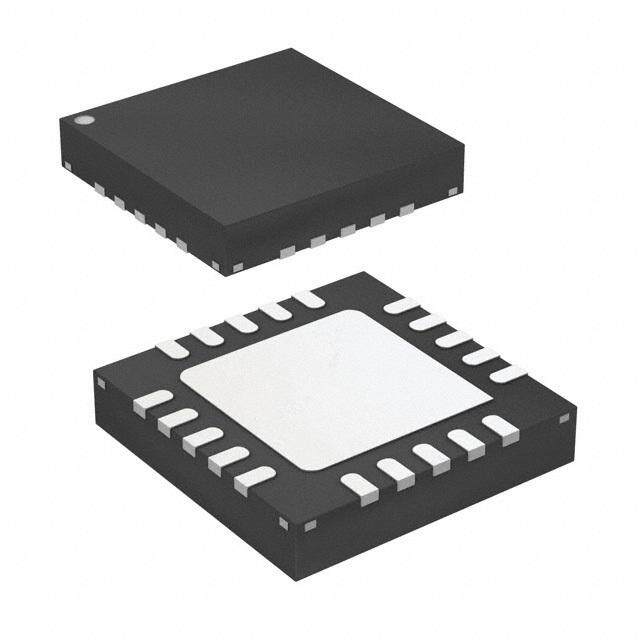
| 描述 | IC TRANSMITTER ASK SOT23-8射频发射器 300MHz To 450MHz ASK FSK Superhtrdyne Rec |
| 产品分类 | |
| 品牌 | Maxim Integrated |
| 产品手册 | |
| 产品图片 |
|
| rohs | 符合RoHS无铅 / 符合限制有害物质指令(RoHS)规范要求 |
| 产品系列 | RF集成电路,射频发射器,Maxim Integrated MAX7044AKA+T- |
| 数据手册 | |
| 产品型号 | MAX7044AKA+T |
| 产品培训模块 | http://www.digikey.cn/PTM/IndividualPTM.page?site=cn&lang=zhs&ptm=25703http://www.digikey.cn/PTM/IndividualPTM.page?site=cn&lang=zhs&ptm=25705 |
| 产品目录页面 | |
| 产品种类 | 射频发射器 |
| 传输供电电流 | 7.7 mA |
| 其它名称 | MAX7044AKA+TCT |
| 其它有关文件 | |
| 功率-输出 | 12.5dBm |
| 包装 | 剪切带 (CT) |
| 商标 | Maxim Integrated |
| 噪声系数 | - 91 dBc |
| 天线连接器 | PCB,表面贴装 |
| 存储容量 | - |
| 安装风格 | SMD/SMT |
| 封装 | Reel |
| 封装/外壳 | SOT-23-8 |
| 封装/箱体 | SOT-23-8 |
| 工作温度 | -40°C ~ 125°C |
| 工作电源电压 | 2.1 V to 3.6 V |
| 工作频率 | 300 MHz to 450 MHz |
| 工厂包装数量 | 2500 |
| 应用 | RKE,TPM,安全系统 |
| 应用说明 | 点击此处下载产品Datasheet点击此处下载产品Datasheet点击此处下载产品Datasheet点击此处下载产品Datasheet点击此处下载产品Datasheet点击此处下载产品Datasheet点击此处下载产品Datasheet点击此处下载产品Datasheet点击此处下载产品Datasheet点击此处下载产品Datasheet点击此处下载产品Datasheet点击此处下载产品Datasheet点击此处下载产品Datasheet点击此处下载产品Datasheet点击此处下载产品Datasheet点击此处下载产品Datasheet |
| 数据接口 | PCB,表面贴装 |
| 数据速率(最大值) | 100kbps |
| 最大工作温度 | + 125 C |
| 最小工作温度 | - 40 C |
| 标准包装 | 1 |
| 特性 | - |
| 电压-电源 | 2.1 V ~ 3.6 V |
| 电流-传输 | 14mA |
| 电源电压-最大 | 3.6 V |
| 电源电压-最小 | 2.1 V |
| 电源电流 | 7.7 mA |
| 类型 | ASK Transmitter |
| 系列 | MAX7044 |
| 调制或协议 | ASK,OOK |
| 调制格式 | ASK, OOK |
| 零件号别名 | MAX7044 |
| 频率 | 300MHz ~ 450MHz |


- 商务部:美国ITC正式对集成电路等产品启动337调查
- 曝三星4nm工艺存在良率问题 高通将骁龙8 Gen1或转产台积电
- 太阳诱电将投资9.5亿元在常州建新厂生产MLCC 预计2023年完工
- 英特尔发布欧洲新工厂建设计划 深化IDM 2.0 战略
- 台积电先进制程称霸业界 有大客户加持明年业绩稳了
- 达到5530亿美元!SIA预计今年全球半导体销售额将创下新高
- 英特尔拟将自动驾驶子公司Mobileye上市 估值或超500亿美元
- 三星加码芯片和SET,合并消费电子和移动部门,撤换高东真等 CEO
- 三星电子宣布重大人事变动 还合并消费电子和移动部门
- 海关总署:前11个月进口集成电路产品价值2.52万亿元 增长14.8%


PDF Datasheet 数据手册内容提取
EVALUATION KIT AVAILABLE MAX7044 300MHz to 450MHz High-Efficiency, Crystal-Based +13dBm ASK Transmitter General Description Features The MAX7044 crystal-referenced phase-locked-loop ● +2.1V to +3.6V Single-Supply Operation (PLL) VHF/UHF transmitter is designed to transmit ● OOK/ASK Transmit Data Format OOK/ASK data in the 300MHz to 450MHz frequency range. The MAX7044 supports data rates up to 100kbps, ● Up to 100kbps Data Rate and provides output power up to +13dBm into a 50Ω load ● +13dBm Output Power into 50Ω Load while only drawing 7.7mA at 2.7V. ● Low 7.7mA (typ) Operating Supply Current* The crystal-based architecture of the MAX7044 eliminates ● Uses Small, Low-Cost Crystal many of the common problems with SAW-based transmitters ● Small 3mm x 3mm 8-Pin SOT23 Package by providing greater modulation depth, faster frequency settling, higher tolerance of the transmit frequency, and ● Fast-On Oscillator: 250μs Startup Time reduced temperature dependence. The MAX7044 also features a low supply voltage of +2.1V to +3.6V. These Applications improvements enable better overall receiver performance ● Remote Keyless Entry (RKE) when using the MAX7044 together with a superheterodyne ● Tire-Pressure Monitoring (TPM) receiver such as the MAX1470 or MAX1473. ● Security Systems A simple, single-input data interface and a buffered ● Garage Door Openers clock-out signal at 1/16th the crystal frequency make the ● RF Remote Controls MAX7044 compatible with almost any microcontroller or ● Wireless Game Consoles code-hopping generator. ● Wireless Computer Peripherals ● Wireless Sensors The MAX7044 is available in an 8-pin SOT23 package and is specified over the -40°C to +125°C automotive Ordering Information temperature range. PIN- TOP PART TEMP RANGE PACKAGE MARK MAX7044AKA+T -40°C to +125°C 8 SOT23 AEJW *At 50% duty cycle (315MHz, 2.7V supply, +13dBm output power). +Denotes a lead(Pb)-free/RoHS-compliant package. T = Tape and reel. Typical Application Circuit Pin Configuration TOP VIEW 3.0V fXTAL 3.0V 1 8 XTAL1 XTAL2 + XTAL1 1 8 XTAL2 100nF 220pF 680pF 2 7 GND VDD 100nF GND 2 7 VDD MAX7044 MAX7044 3 6 PAGND 3 6 DATA ANTENNA PAGND DATA DATA INPUT CLOCK PAOUT 4 5 CLKOUT 4 PAOUTCLKOUT 5 OUTPUT (fCLKOUT = SOT23 fXTAL/16) 19-3221; Rev 5; 4/17
MAX7044 300MHz to 450MHz High-Efficiency, Crystal-Based +13dBm ASK Transmitter Absolute Maximum Ratings VDD to GND .........................................................-0.3V to +4.0V Storage Temperature Range ............................-60°C to +150°C All Other Pins to GND ..............................-0.3V to (VDD + 0.3V) Junction Temperature ......................................................+150°C Continuous Power Dissipation (TA = +70°C) Lead Temperature (soldering, 10s) .................................+300°C 8-Pin SOT23 (derate 8.9mW/°C above +70°C) ..........714mW Soldering Temperature (reflow) .......................................+260°C Operating Temperature Range .........................-40°C to +125°C Stresses beyond those listed under “Absolute Maximum Ratings” may cause permanent damage to the device. These are stress ratings only, and functional operation of the device at these or any other conditions beyond those indicated in the operational sections of the specifications is not implied. Exposure to absolute maximum rating conditions for extended periods may affect device reliability. Electrical Characteristics (Typical Application Circuit, all RF inputs and outputs are referenced to 50Ω, VDD = +2.1V to +3.6V, TA = -40°C to +125°C, unless otherwise noted. Typical values are at VDD = +2.7V, TA = +25°C, unless otherwise noted.) (Note 1) PARAMETER SYMBOL CONDITIONS MIN TYP MAX UNITS SYSTEM PERFORMANCE Supply Voltage VDD 2.1 3.6 V VDATA at 50% duty 7.7 14.1 cycle (Notes 3, 4) fRF = 315MHz PA on (Note 5) 13.8 25.4 Supply Current PA off (Note 6) 1.7 2.8 (Note 2) IDD VDATA at 50% duty 8.0 14.4 mA cycle (Notes 3, 4) fRF = 433MHz PA on (Note 5) 14.0 25.7 PA off (Note 6) 1.9 3.1 VDATA < VIL for TA < +25°C 40 130 Standby Current ISTDBY more than WAIT nA time (Notes 4, 7) TA < +125°C 550 2900 Frequency Range (Note 4) fRF 300 450 MHz Data Rate (Note 4) 0 100 kbps Modulation Depth (Note 8) ON to OFF POUT ratio 90 dB TA = +25°C, 9.6 12.5 15.4 VDD = +2.7V O(Nuottpeust 4P,o 5w)er, PA On POUT f4R5F0 M= H30z0MHz to TVAD D= =+ 1+225.1°CV, 5.9 9.0 12.0 dBm TA = -40°C, 13.1 15.8 18.5 VDD = +3.6V Oscillator settled to within 50kHz 220 Turn-On Time tON µs Oscillator settled to within 5kHz 450 Transmit Efficiency with CW fRF = 315MHz 48 % (Notes 5, 9) fRF = 433MHz 47 Transmit Efficiency with 50% OOK fRF = 315MHz 43 % (Notes 3, 9) fRF = 433MHz 41 www.maximintegrated.com Maxim Integrated │ 2
MAX7044 300MHz to 450MHz High-Efficiency, Crystal-Based +13dBm ASK Transmitter Electrical Characteristics (continued) (Typical Application Circuit, all RF inputs and outputs are referenced to 50Ω, VDD = +2.1V to +3.6V, TA = -40°C to +125°C, unless otherwise noted. Typical values are at VDD = +2.7V, TA = +25°C, unless otherwise noted.) (Note 1) PARAMETER SYMBOL CONDITIONS MIN TYP MAX UNITS PHASE-LOCKED LOOP (PLL) VCO Gain 330 MHz/V fOFFSET = 100kHz -84 fRF = 315MHz fOFFSET = 1MHz -91 Phase Noise dBc/Hz fOFFSET = 100kHz -82 fRF = 433MHz fOFFSET = 1MHz -89 fRF = 315MHz -50 Maximum Carrier Harmonics dBc fRF = 433MHz -50 fRF = 315MHz -74 Reference Spur dBc fRF = 433MHz -80 Loop Bandwidth 1.6 MHz Crystal Frequency fXTAL fRF/32 MHz Frequency Pulling by VDD 3 ppm/V Crystal Load Capacitance 3 pF DATA INPUT Data Input High VIH V0D.2D5 - V Data Input Low VIL 0.25 V Maximum Input Current 10 µA Pulldown Current 10 µA CLKOUT OUTPUT Output Voltage Low VOL ISINK = 650µA (Note 4) 0.25 V Output Voltage High VOH ISOURCE = 350µA (Note 4) V0D.2D5 - V Load Capacitance CLOAD (Note 4) 10 pF CLKOUT Frequency fXTAL/16 Hz Note 1: Supply current, output power, and efficiency are greatly dependent on board layout and PAOUT match. Note 2: Production tested at TA = +25°C with fRF = 300MHz and 450MHz. Guaranteed by design and characterization over tem- perature and frequency. Note 3: 50% duty cycle at 10kbps with Manchester coding. Note 4: Guaranteed by design and characterization, not production tested. Note 5: PA output is turned on in test mode by VDATA = VDD/2 + 100mV. Note 6: PA output is turned off in test mode by VDATA = VDD/2 - 100mV. Note 7: Wait time: tWAIT = (216 x 32)/fRF. Note 8: Generally limited by PCB layout. Note 9: VDATA = VIH. Efficiency = POUT/(VDD x IDD). www.maximintegrated.com Maxim Integrated │ 3
MAX7044 300MHz to 450MHz High-Efficiency, Crystal-Based +13dBm ASK Transmitter Typical Operating Characteristics (Typical Application Circuit, VDD = +2.7V, TA = +25°C, unless otherwise noted.) (Note 1) SUPPLY CURRENT SUPPLY CURRENT SUPPLY CURRENT vs. SUPPLY VOLTAGE vs. SUPPLY VOLTAGE vs. SUPPLY VOLTAGE A) 122913 PfRAF O= N315MHz TA = -40°C MAX7044 toc01 A) 111123 PfRAF 5=0 3%1 5DMUHTzY CYCLE AT 10kHz MAX7044 toc02 A) 2202 PfRAF O= N433MHz TA = -40°C MAX7044 toc03 m m m 18 T ( T ( TA = +25°C T ( N 17 N 10 N RE TA = +25°C RE RE 16 UR 15 UR 9 TA = -40°C UR TA = +25°C PPLY C 13 TA = +85°C PPLY C 8 TA = +85°C PPLY C 14 TA = +85°C SU 11 SU 7 SU 12 TA = +125°C TA = +125°C 9 6 TA = +125°C 10 7 5 8 2.1 2.4 2.7 3.0 3.3 3.6 2.1 2.4 2.7 3.0 3.3 3.6 2.1 2.4 2.7 3.0 3.3 3.6 SUPPLY VOLTAGE (V) SUPPLY VOLTAGE (V) SUPPLY VOLTAGE (V) SUPPLY CURRENT OUTPUT POWER OUTPUT POWER vs. SUPPLY VOLTAGE vs. SUPPLY VOLTAGE vs. SUPPLY VOLTAGE 1134 PfRAF 5=0 4%3 3DMUHTzY CYCLE AT 10kHz MAX7044 toc04 1168 PfRAF O= N315MHz TA = -40°C MAX7044 toc05 1168 PfRAF O= N433MHz TA = -40°C MAX7044 toc06 SUPPLY CURRENT (mA) 11189012 TA = +25°C TA =T +A1 =25 -°4C0°CTA = +85°C OUTPUT POWER (dBm) 111042 TA = +25°CTA = +125°C TA = +85°C OUTPUT POWER (dBm) 111042 TTAA == ++12255°°CC TA = +85°C 7 6 8 8 2.1 2.4 2.7 3.0 3.3 3.6 2.1 2.4 2.7 3.0 3.3 3.6 2.1 2.4 2.7 3.0 3.3 3.6 SUPPLY VOLTAGE (V) SUPPLY VOLTAGE (V) SUPPLY VOLTAGE (V) REFERENCE SPUR MAGNITUDE FREQUENCY STABILITY TRANSMIT POWER EFFICIENCY vs. SUPPLY VOLTAGE vs. SUPPLY VOLTAGE vs. SUPPLY VOLTAGE NCE SPUR MAGNITUDE (dBc) ----77774620 RfREFF =E 4R3E3NMCHEz SPUR = fRF fXTAL MAX7044 toc07 QUENCY STABILITY (ppm) -11023 fRF f=R F4 3=3 3M1H5zMHz MAX7044 toc08 MIT POWER EFFICIENCY (%) 455667505050 PfRAF TO=A N3 =1 5+M25H°zC TA = -40°C MAX7044 toc09 REFERE -78 fRF = 315MHz FRE -2 TRANS 3450 TA = +125°C TA = +85°C -80 -3 30 2.1 2.4 2.7 3.0 3.3 3.6 2.1 2.4 2.7 3.0 3.3 3.6 2.1 2.4 2.7 3.0 3.3 3.6 SUPPLY VOLTAGE (V) SUPPLY VOLTAGE (V) SUPPLY VOLTAGE (V) www.maximintegrated.com Maxim Integrated │ 4
MAX7044 300MHz to 450MHz High-Efficiency, Crystal-Based +13dBm ASK Transmitter Typical Operating Characteristics (continued) (Typical Application Circuit, VDD = +2.7V, TA = +25°C, unless otherwise noted.) (Note 1) TRANSMIT POWER EFFICIENCY TRANSMIT POWER EFFICIENCY TRANSMIT POWER EFFICIENCY vs. SUPPLY VOLTAGE vs. SUPPLY VOLTAGE vs. SUPPLY VOLTAGE NCY (%) 556050 PfRAF T 5=A0 3%=1 5-D4M0UH°TCzY CYCLE AT 1T0Ak H=z +25°C MAX7044 toc10 NCY (%) 667050 PfRAF O= N433MTHAz = +25°C TA = -40°C MAX7044 toc11 NCY (%) 556500 PfRTAFA 5==0 4%-43 03D°MUCHTzY CYCLE AT 10kHz TA = +25°C MAX7044 toc12 E E E CI CI CI 45 FI 45 FI 55 FI F F F ER E 40 ER E 50 ER E 40 OW OW OW 35 TA = +85°C MIT P 35 TA = +85°C MIT P 45 TA = +85°C MIT P 30 TRANS 2350 TA = +125°C TRANS 3450 TA = +125°C TRANS 2250 TA = +125°C 20 30 15 2.1 2.4 2.7 3.0 3.3 3.6 2.1 2.4 2.7 3.0 3.3 3.6 2.1 2.4 2.7 3.0 3.3 3.6 SUPPLY VOLTAGE (V) SUPPLY VOLTAGE (V) SUPPLY VOLTAGE (V) SUPPLY CURRENT AND OUTPUT POWER PHASE NOISE vs. OFFSET FREQUENCY vs. EXTERNAL RESISTOR SUPPLY CURRENT vs. OUTPUT POWER ---654000 MAX7044 toc13 1168 POWEMRAX7044 toc14 1126 1158 fRF = 315MHz MAX7044 toc15 PHASE NOISE (dBc/Hz)--11---1098700000 SUPPLY CURRENT (mA) 11168024 CURRENT --04884 OUTPUT POWER (dBm) SUPPLY CURRENT (mA) 1629 PA ON -120 3 -130 4 fRF = 315MHz -12 50% DUTY CYCLE PA ON -140 2 -16 0 0.01 0.1 1 10 100 1 10 0 1 10 100 1000 10,000 -10 -6 -2 2 6 10 14 OFFSET FREQUENCY (kHz) EXTERNAL RESISTOR (Ω) OUTPUT POWER (dBm) AM DEMODULATION OF PA OUTPUT FREQUENCY SETTLING TIME DATA RATE = 100kHz OUTPUT SPECTRUM MAX7044 toc16 MAX7044 toc17 0dB MAX7044 toc18 fRF = 315MHz 50kHz/ 5dB/ 10dB/ div div div 25µs/div 3.2µs/div 100MHz/div www.maximintegrated.com Maxim Integrated │ 5
MAX7044 300MHz to 450MHz High-Efficiency, Crystal-Based +13dBm ASK Transmitter Typical Operating Characteristics (continued) (Typical Application Circuit, VDD = +2.7V, TA = +25°C, unless otherwise noted.) (Note 1) CLKOUT SPUR MAGNITUDE vs. SUPPLY VOLTAGE dBc) --4430 fRF = 315MHz MAX7044 toc19 E ( D U T NI -46 G A M R U P -49 S T U O LK -52 C -55 2.1 2.4 2.7 3.0 3.3 3.6 SUPPLY VOLTAGE (V) Pin Description PIN NAME FUNCTION 1 XTAL1 1st Crystal Input. fXTAL = fRF/32. 2 GND Ground. Connect to system ground. 3 PAGND Ground for the Power Amplifier (PA). Connect to system ground. Power-Amplifier Output. The PA output requires a pullup inductor to the supply voltage, which can be 4 PAOUT part of the output-matching network to an antenna. 5 CLKOUT Buffered Clock Output. The frequency of CLKOUT is fXTAL/16. 6 DATA OOK Data Input. DATA also controls the power-up state. See the Shutdown Mode section. 7 VDD Supply Voltage. Bypass to GND with a 100nF capacitor as close as possible to the pin. 8 XTAL2 2nd Crystal Input. fXTAL = fRF/32. Functional Diagram Detailed Description The MAX7044 is a highly integrated ASK transmitter operating over the 300MHz to 450MHz frequency band. DATA MAX7044 The IC requires only a few external components to VDD complete a transmit solution. The MAX7044 includes a DATA GND complete PLL and a highly efficient power amplifier. The ACTIVITY DETECTOR PA PAOUT device is automatically placed into a low-power shutdown mode and powers up when data is detected on the data PAGND input. Once power is supplied to VDD, the DATA pin must LOCK DETECT 32x PLL receive at least one logic pulse (low-high-low transition) in order to properly initialize the device. XTAL1 CRYSTAL- Shutdown Mode OSCILLATOR /16 CLKOUT XTAL2 DRIVER The MAX7044 has an automatic shutdown mode that places the device in low-power mode if the DATA input has not toggled for a specific amount of time (wait time). www.maximintegrated.com Maxim Integrated │ 6
MAX7044 300MHz to 450MHz High-Efficiency, Crystal-Based +13dBm ASK Transmitter The wait time is equal to 216 clock cycles of the crystal. When the output matching network is properly tuned, the This equates to a wait time of approximately 6.66ms for power amplifier transmits power with high efficiency. a 315MHz RF frequency and 4.84ms for a 433MHz RF The Typical Application Circuit delivers +13dBm at +2.7V frequency. For other frequencies, calculate the wait time supply with 7.7mA of supply current. Thus, the overall with the following equation: efficiency is 48% with the efficiency of the power amplifier itself greater than 54%. 216x32 tWAIT= Buffered Clock Output fRF The MAX7044 provides a buffered clock output (CLKOUT) where tWAIT is the wait time to shutdown and fRF is the for easy interface to a microcontroller or frequency-hop- RF transmit frequency. ping generator. The frequency of CLKOUT is 1/16 the When the device is in shutdown, a rising edge on DATA crystal frequency. For a 315MHz RF transmit frequency, initiates the warm up of the crystal and PLL. The crystal a crystal of 9.84375MHz is used, giving a clock output of and PLL must have 220μs settling time before data can 615.2kHz. For a 433.92MHz RF frequency, a crystal of be transmitted. The 220μs turn-on time of the MAX7044 13.56MHz is used for a clock output of 847.5kHz. is dominated by the crystal oscillator startup time. Once The clock output is inactive when the device is in shut- the oscillator is running, the 1.6MHz PLL loop bandwidth down mode. The device is placed in shutdown mode allows fast frequency recovery during power amplifier by the internal data activity detector (see the Shutdown toggling. Mode section). Once data is detected on the data input, When the device is operating, each edge on the data line the clock output is stable after approximately 220μs. resets an internal counter to zero and it begins to count Applications Information again. If no edges are detected on the data line, the counter reaches the end-of-count (216 clock cycles) and Output Power Adjustment places the device in shutdown mode. If there is an edge It is possible to adjust the output power down to -15dBm on the data line before the counter hits the end of count, with the addition of a resistor (see RPWRADJ in Figure 1). the counter is reset and the process starts over. It may The addition of the power adjust resistor also reduces be necessary to keep the power amplifier on steadily for power consumption. See the Supply Current and Output testing and debugging purposes. To do this, set the DATA Power vs. External Resistor and Supply Current vs. Output pin voltage slightly above the midpoint between VDD and Power graphs in the Typical Operating Characteristics ground (VDD/2 + 100mV). section. It is imperative to add both a low-frequency and a high-frequency decoupling capacitor as shown in Figure 1. Phase-Locked Loop The PLL block contains a phase detector, charge pump, Crystal Oscillator integrated loop filter, VCO, asynchronous 32x clock The crystal oscillator in the MAX7044 is designed to divider, and crystal oscillator. This PLL requires no external present a capacitance of approximately 3pF between the components. The relationship between the carrier and XTAL1 and XTAL2 pins. If a crystal designed to oscillate crystal frequency is given by: fXTAL = fRF/32 The lock-detect circuit prevents the power amplifier from 3.0V transmitting until the PLL is locked. In addition, the device shuts down the power amplifier if the reference frequency fXTAL 3.0V is lost. 100nF 1 8 RPWRADJ XTAL1 XTAL2 Power Amplifier (PA) 2 7 The PA of the MAX7044 is a high-efficiency, open-drain, GND VDD 100nF switch-mode amplifier. With a proper output matching 220pF 680pF MAX7044 network, the PA can drive a wide range of impedances, ANTENNA 3 PAGND DATA 6 DATA INPUT including the small-loop PCB trace antenna and any 50Ω CLOCK antenna. The output-matching network for an antenna 4 PAOUTCLKOUT 5 OUTPUT with a characteristic impedance of 50Ω is shown in the (fCLKOUT = Typical Application Circuit. The output matching network fXTAL/16) suppresses the carrier harmonics and transforms the antenna impedance to an optimal impedance at PAOUT, which is about 125Ω. Figure 1. Output Power Adjustment Circuit www.maximintegrated.com Maxim Integrated │ 7
MAX7044 300MHz to 450MHz High-Efficiency, Crystal-Based +13dBm ASK Transmitter with a different load capacitance is used, the crystal is Output Matching to pulled away from its intended operating frequency, thus PCB Loop Antenna introducing an error in the reference frequency. Crystals In some applications, the MAX7044 power amplifier output designed to operate with higher differential load capacitance has to be impedance matched to a small-loop antenna. always pull the reference frequency higher. For example, The antenna is usually fabricated out of a copper trace on a 9.84375MHz crystal designed to operate with a 10pF a PCB in a rectangular, circular, or square pattern. The load capacitance oscillates at 9.84688MHz with the antenna will have an impedance that consists of a lossy MAX7044, causing the transmitter to be transmitting component and a radiative component. To achieve high at 315.1MHz rather than 315.0MHz, an error of about radiating efficiency, the radiative component should be as 100kHz, or 320ppm. high as possible, while minimizing the lossy component. In actuality, the oscillator pulls every crystal. The crystal’s In addition, the loop antenna will have an inherent loop natural frequency is really below its specified frequency, inductance associated with it (assuming the antenna but when loaded with the specified load capacitance, the is terminated to ground). For example, in a typical crystal is pulled and oscillates at its specified frequency. application, the radiative impedance is less than 0.5Ω, the This pulling is already accounted for in the specification of lossy impedance is less than 0.7Ω, and the inductance is the load capacitance. Additional pulling can be calculated approximately 50nH to 100nH. if the electrical parameters of the crystal are known. The The objective of the matching network is to match the frequency pulling is given by: power amplifier output to the small-loop antenna. The matching components thus transform the low radiative fp=Cm 1 − 1 x10⁶ and resistive parts of the antenna into the much higher 2 Ccase+Cload Ccase+Cspec value of the PA output. This gives higher efficiency. The low radiative and lossy components of the small-loop where: antenna result in a higher Q matching network than the fp is the amount the crystal frequency is pulled in ppm. 50Ω network; thus, the harmonics are lower. Cm is the motional capacitance of the crystal. Layout Considerations Ccase (or Co) is the vendor-specified case capacitance of the crystal. A properly designed PCB is an essential part of any Cspec is the specified load capacitance. RF/microwave circuit. At the power amplifier output, use controlled-impedance lines and keep them as short Cload is the actual load capacitance. as possible to minimize losses and radiation. At high When the crystal is loaded as specified (i.e., Cload = Cspec) frequencies, trace lengths that are approximately 1/20 the the frequency pulling equals zero. wavelength or longer become antennas. For example, a Output Matching to 50Ω 2in trace at 315MHz can act as an antenna. When matched to a 50Ω system, the MAX7044 PA is Keeping the traces short also reduces parasitic capable of delivering up to +13dBm of output power inductance. Generally, 1in of PCB trace adds about 20nH at VDD = 2.7V. The output of the PA is an open-drain of parasitic inductance. The parasitic inductance can transistor that requires external impedance matching have a dramatic effect on the effective inductance. For and pullup inductance for proper biasing. The pullup example, a 0.5in trace connecting a 100nH inductor adds inductance from PA to VDD serves three main purposes: an extra 10nH of inductance, or 10%. it resonates the capacitance of the PA output, provides To reduce the parasitic inductance, use wider traces and a biasing for the PA, and becomes a high-frequency choke solid ground or power plane below the signal traces. Using to reduce the RF energy coupling into VDD. The recom- a solid ground plane can reduce the parasitic inductance mended output-matching network topology is shown in from approximately 20nH/in to 7nH/in. Also, use low- the Typical Application Circuit. The matching network inductance connections to ground on all GND pins, and transforms the 50Ω load to approximately 125Ω at the output of the PA in addition to forming a bandpass filter place decoupling capacitors close to all VDD connections. that provides attenuation for the higher order harmonics. www.maximintegrated.com Maxim Integrated │ 8
MAX7044 300MHz to 450MHz High-Efficiency, Crystal-Based +13dBm ASK Transmitter Chip Information Package Information PROCESS: CMOS For the latest package outline information and land patterns (footprints), go to www.maximintegrated.com/packages. Note that a “+”, “#”, or “-” in the package code indicates RoHS status only. Package drawings may show a different suffix character, but the drawing pertains to the package regardless of RoHS status. PACKAGE PACKAGE OUTLINE LAND TYPE CODE NO. PATTERN NO. 8 SOT23 K8SN+1 21-0078 90-0176 www.maximintegrated.com Maxim Integrated │ 9
MAX7044 300MHz to 450MHz High-Efficiency, Crystal-Based +13dBm ASK Transmitter Revision History REVISION REVISION PAGES DESCRIPTION NUMBER DATE CHANGED Changed part number in Ordering Information to lead-free and made a correction 3 6/09 1, 7 in the Power Amplifier (PA) section Deleted Maximum Crystal Inductance spec and Note 9 from the Electrical 4 2/11 Characteristics table and updated the Absolute Maximum Ratings, Shutdown 2, 3, 7, 8 Mode, and Crystal Oscillator sections 5 5/17 Updated Detailed Description section 6 For pricing, delivery, and ordering information, please contact Maxim Direct at 1-888-629-4642, or visit Maxim Integrated’s website at www.maximintegrated.com. Maxim Integrated cannot assume responsibility for use of any circuitry other than circuitry entirely embodied in a Maxim Integrated product. No circuit patent licenses are implied. Maxim Integrated reserves the right to change the circuitry and specifications without notice at any time. The parametric values (min and max limits) shown in the Electrical Characteristics table are guaranteed. Other parametric values quoted in this data sheet are provided for guidance. Maxim Integrated and the Maxim Integrated logo are trademarks of Maxim Integrated Products, Inc. © 2017 Maxim Integrated Products, Inc. │ 10
Mouser Electronics Authorized Distributor Click to View Pricing, Inventory, Delivery & Lifecycle Information: M axim Integrated: MAX7044AKA+T MAX7044AKA-T