ICGOO在线商城 > 射频/IF 和 RFID > RF 发射器 > CC1150RSTR
 Datasheet下载
- 型号: CC1150RSTR
- 制造商: Texas Instruments
- 库位|库存: xxxx|xxxx
- 要求:
| 数量阶梯 | 香港交货 | 国内含税 |
| +xxxx | $xxxx | ¥xxxx |
查看当月历史价格
查看今年历史价格
CC1150RSTR产品简介:
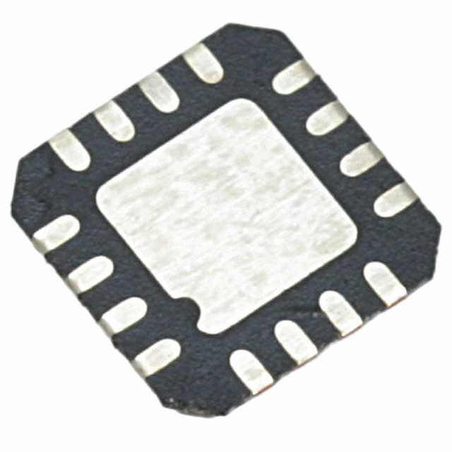
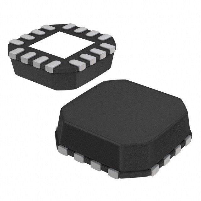
ICGOO电子元器件商城为您提供CC1150RSTR由Texas Instruments设计生产,在icgoo商城现货销售,并且可以通过原厂、代理商等渠道进行代购。 CC1150RSTR价格参考。Texas InstrumentsCC1150RSTR封装/规格:RF 发射器, RF Transmitter 2-FSK, ASK, GFSK, MSK, OOK 300MHz ~ 348MHz, 400MHz ~ 464MHz, 800MHz ~ 928MHz -30dBm ~ 10dBm 500kBaud PCB, Surface Mount Antenna 16-QFN。您可以下载CC1150RSTR参考资料、Datasheet数据手册功能说明书,资料中有CC1150RSTR 详细功能的应用电路图电压和使用方法及教程。
Texas Instruments(德州仪器)的CC1150RSTR是一款高性能、低功耗的RF发射器芯片,属于Sub-1 GHz无线通信解决方案。该芯片广泛应用于需要远距离、低功耗无线传输的场景。

典型应用场景包括:
1. 工业无线传感器网络:用于远程监控温度、湿度、压力等参数,适用于工厂自动化和环境监测系统。
2. 自动抄表系统(AMI):在水表、气表、电表等智能计量设备中,实现稳定可靠的无线数据上传。
3. 家庭与楼宇自动化:如无线照明控制、安防系统(门窗传感器、报警器)、智能门锁等,支持长距离穿透墙体通信。
4. 无线遥控装置:应用于车库门控制器、远程开关、遥控钥匙等消费类电子产品。
5. 农业与环境监测:部署于农田或偏远区域的无线传感节点,实现土壤湿度、气象数据的远程采集。

CC1150RSTR支持多种调制方式(如FSK、GFSK、OOK),工作频段灵活(300–348 MHz、378–486 MHz、720–820 MHz),可适应不同地区法规要求。其小尺寸QFN封装(RSTR)便于集成到紧凑型设备中,并与TI的MCU(如MSP430、CC系列)无缝配合,构建完整的低功耗无线系统。

综上,CC1150RSTR适用于对通信距离、稳定性及功耗有较高要求的中低速无线传输应用,尤其适合工业与物联网领域的远程控制与数据采集系统。
| 参数 | 数值 |
| 产品目录 | |
| 描述 | IC RF TX SNGL-CHIP LP 16-QFN射频发射器 UHF TRANSMITTER TAPE AND REEL |
| 产品分类 | |
| 品牌 | Texas Instruments |
| 产品手册 | |
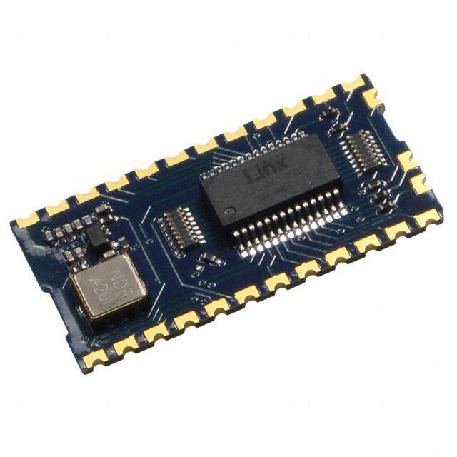
| 产品图片 |
|
| rohs | 符合RoHS无铅 / 符合限制有害物质指令(RoHS)规范要求 |
| 产品系列 | RF集成电路,射频发射器,Texas Instruments CC1150RSTR- |
| 数据手册 | |
| 产品型号 | CC1150RSTR |
| 产品培训模块 | http://www.digikey.cn/PTM/IndividualPTM.page?site=cn&lang=zhs&ptm=26085 |
| 产品目录页面 | |
| 产品种类 | 射频发射器 |
| 其它名称 | 296-19584-1 |
| 制造商产品页 | http://www.ti.com/general/docs/suppproductinfo.tsp?distId=10&orderablePartNumber=CC1150RSTR |
| 功率-输出 | -30dBm ~ 10dBm |
| 包装 | 剪切带 (CT) |
| 商标 | Texas Instruments |
| 天线连接器 | PCB,表面贴装 |
| 存储容量 | - |
| 安装风格 | SMD/SMT |
| 封装 | Reel |
| 封装/外壳 | 16-QFN |
| 封装/箱体 | VQFNP-16 |
| 工作温度 | -40°C ~ 85°C |
| 工作电源电压 | 1.8 V, 2.5 V, 3.3 V |
| 工作频率 | 915 MHz |
| 工厂包装数量 | 2500 |
| 应用 | AMR,ISM,RKE,SRD |
| 数据接口 | PCB,表面贴装 |
| 数据速率(最大值) | 500 kBaud |
| 最大工作温度 | + 85 C |
| 最小工作温度 | - 40 C |
| 标准包装 | 1 |
| 特性 | - |
| 电压-电源 | 1.8 V ~ 3.6 V |
| 电流-传输 | 28.1mA @ 10 dBm |
| 类型 | Transmitter |
| 系列 | CC1150 |
| 调制或协议 | 2-FSK,ASK,GFSK,MSK,OOK |
| 配用 | /product-detail/zh/CC1150EMK-433/296-30813-ND/1690517/product-detail/zh/CC1150EMK-868/296-30814-ND/1690518 |
| 频率 | 300MHz ~ 348MHz, 400MHz ~ 464MHz, 800MHz ~ 928MHz |


- 商务部:美国ITC正式对集成电路等产品启动337调查
- 曝三星4nm工艺存在良率问题 高通将骁龙8 Gen1或转产台积电
- 太阳诱电将投资9.5亿元在常州建新厂生产MLCC 预计2023年完工
- 英特尔发布欧洲新工厂建设计划 深化IDM 2.0 战略
- 台积电先进制程称霸业界 有大客户加持明年业绩稳了
- 达到5530亿美元!SIA预计今年全球半导体销售额将创下新高
- 英特尔拟将自动驾驶子公司Mobileye上市 估值或超500亿美元
- 三星加码芯片和SET,合并消费电子和移动部门,撤换高东真等 CEO
- 三星电子宣布重大人事变动 还合并消费电子和移动部门
- 海关总署:前11个月进口集成电路产品价值2.52万亿元 增长14.8%


PDF Datasheet 数据手册内容提取
Product Sample & Technical Tools & Support & Folder Buy Documents Software Community CC1150 SWRS037B–JANUARY2006–REVISEDMARCH2015 CC1150 Low Power Sub-1 GHz RF Transmitter 1 Device Overview 1.1 Features 1 • SmallSize • 64-byteTXDataFIFO – QLP4-mm ×4-mmPackage,16Pins • SuitedforSystemsCompliantwithEN300220 • TrueSingleChipUHFRFTransmitter andFCCCFRPart15 • FrequencyBands • ManyPowerfulDigitalFeaturesAllowaHigh- performanceRFsystemtobemadeUsingan – 300to348MHz InexpensiveMicrocontroller – 400to464MHz • EfficientSPIinterface:AllRegistersCanbe – 800to928MHz ProgrammedWithOne"Burst"Transfer • ProgrammableDataRateUpto500kBaud • IntegratedAnalogTemperatureSensor • LowCurrentConsumption • Lead-free “Green”Package • ProgrammableOutputPowerUpto+10dBmfor • FlexibleSupportforPacketOrientedSystems AllSupportedFrequencies – On-chipSupportforSync-WordInsertion, • ProgrammableBasebandModulator FlexiblePacketLengthandAutomaticCRC • IdealForMulti-channelOperation Handling • VeryFewExternalComponents • OOKandFlexibleASKShapingSupported – CompletelyOn-chipFrequencySynthesizer • 2-FSK,GFSKandMSKSupported – NoExternalFiltersNeeded • OptionalAutomaticWhiteningofData • ConfigurablePacketHandlingHardware • SupportforAsynchronousTransparentTransmit • SuitableforFrequencyHoppingSystemsDuetoa ModeforBackwardsCompatibilitywithExisting FastSettlingFrequencySynthesizer RadioCommunicationProtocols • OptionalForwardErrorCorrectionwithInterleaving 1.2 Applications • Ultra-lowPowerUHFWirelessTransmitters • LowPowerTelemetry • Operatinginthe315-,433-,868-,and915-MHz • HomeandBuildingAutomation ISM/SRDbands • WirelessAlarmandSecuritySystems • AMR–AutomaticMeterReading • IndustrialMonitoringandControl • ConsumerElectronics • WirelessSensorNetworks • RKE– RemoteKeylessEntry 1.3 Description The CC1150 is a true single-chip UHF transmitter designed for very low power wireless applications. The circuit is mainly intended for the ISM (Industrial, Scientific and Medical) and SRD (Short Range Device) frequency bands at 315-, 433-, 868-, and 915-MHz, but can easily be programmed for operation at other frequenciesinthe300to348MHz,400to464MHzand800to928MHzbands. The RF transmitter is integrated with a highly configurable baseband modulator. The modulator supports various modulation formats and has a configurable data rate up to 500 kBaud. The CC1150 device providesextensivehardwaresupportforpackethandling,databufferingandbursttransmissions. The main operating parameters and the 64-byte transmit FIFO of CC1150 can be controlled via an SPI interface. In a typical system, the CC1150 device will be used together with a microcontroller and a few additionalpassivecomponents. CC1150 is part of the SmartRF™ technology platform based on 0.18-μm CMOS technology from Texas Instruments. 1 AnIMPORTANTNOTICEattheendofthisdatasheetaddressesavailability,warranty,changes,useinsafety-criticalapplications, intellectualpropertymattersandotherimportantdisclaimers.PRODUCTIONDATA.
CC1150 SWRS037B–JANUARY2006–REVISEDMARCH2015 www.ti.com Table1-1.DeviceInformation(1) PARTNUMBER PACKAGE BODYSIZE CC1150 VQFNP(16) 4.00mm×4.00mm (1) Formoreinformation,seeSection8,MechanicalPackagingandOrderableInformation. 1.4 Functional Block Diagram RADIOCONTROL RRFF__NP PA SFYRNETQH ODULATOR FEC/TERLEAVER PACKETHANDLER TXFIFO DIGITALNTERFACETOMCU SSSCCOISLn(KGDO1) BIAS XOSC M N I GDO0(ATEST) I RBIAS XOSC_Q1 XOSC_Q2 2 DeviceOverview Copyright©2006–2015,TexasInstrumentsIncorporated SubmitDocumentationFeedback ProductFolderLinks:CC1150
CC1150 www.ti.com SWRS037B–JANUARY2006–REVISEDMARCH2015 Table of Contents 1 DeviceOverview......................................... 1 5.7 DataRateProgramming............................ 18 .............................................. ................. 1.1 Features 1 5.8 PacketHandlingHardwareSupport 19 ........................................... ................................. 1.2 Applications 1 5.9 ModulationFormats 23 ............................................ .......... 1.3 Description 1 5.10 ForwardErrorCorrectionwithInterleaving 24 ............................ ........................................ 1.4 FunctionalBlockDiagram 2 5.11 RadioControl 26 2 Revision History......................................... 4 5.12 Data FIFO........................................... 29 3 TerminalConfigurationandFunctions.............. 5 5.13 FrequencyProgramming ........................... 31 ......................................... ................................................. 3.1 PinAttributes 5 5.14 VCO 31 4 Specifications ............................................ 6 5.15 VoltageRegulators.................................. 32 .......................... ......................... 4.1 AbsoluteMaximumRatings 6 5.16 OutputPowerProgramming 32 .......................................... .... 4.2 ESDRatings 6 5.17 GeneralPurposeandTestOutputControlPins 33 ................ .. 4.3 RecommendedOperatingConditions 6 5.18 AsynchronousandSynchronousSerialOperation 35 .............................. ............. 4.4 General Characteristics 6 5.19 SystemConsiderationsandGuidelines 36 ................................. .............................................. 4.5 CurrentConsumption 7 5.20 Memory 38 4.6 RF Transmit.......................................... 7 6 Applications,Implementation,andLayout........ 51 ..................................... .............................. 4.7 CrystalOscillator 8 6.1 ApplicationInformation 51 .............. ............................... 4.8 FrequencySynthesizerCharacteristics 8 6.2 DesignRequirements 53 ......................... ..................... 4.9 AnalogTemperatureSensor 9 6.3 PCBLayoutRecommendations 55 4.10 DCCharacteristics ................................... 9 7 DeviceandDocumentationSupport............... 58 .................................... ...................................... 4.11 Power-OnReset 10 7.1 DeviceSupport 58 4.12 ThermalResistanceCharacteristicsforVQFNP 7.2 DocumentationSupport............................. 58 ............................................. Package 10 .......................................... 7.3 Trademarks 59 5 DetailedDescription................................... 11 ..................... 7.4 ElectrostaticDischargeCaution 59 ............................................ 5.1 Overview 11 ............................... 7.5 ExportControlNotice 59 ........................... 5.2 FunctionalBlockDiagram 11 ............................................. 7.6 Glossary 59 ............................. 5.3 ConfigurationOverview 11 8 MechanicalPackagingandOrderable 5.4 ConfigurationSoftware.............................. 12 Information.............................................. 59 5.5 4-wireSerialConfigurationandDataInterface ..... 13 8.1 PackagingInformation .............................. 59 ..... 5.6 MicrocontrollerInterfaceandPinConfiguration 17 Copyright©2006–2015,TexasInstrumentsIncorporated TableofContents 3 SubmitDocumentationFeedback ProductFolderLinks:CC1150
CC1150 SWRS037B–JANUARY2006–REVISEDMARCH2015 www.ti.com 2 Revision History This data manual revision history highlights the changes made to the SWRS037A device-specific data manualtomakeitanSWRS037Brevision. ChangesfromJanuary1,2006toFebruary19,2015 Page • UpdatedRSTpackagetoRGV. .................................................................................................. 58 4 RevisionHistory Copyright©2006–2015,TexasInstrumentsIncorporated SubmitDocumentationFeedback ProductFolderLinks:CC1150
CC1150 www.ti.com SWRS037B–JANUARY2006–REVISEDMARCH2015 3 Terminal Configuration and Functions TheCC1150pinoutisshowninFigure3-1andTable3-1 D R SI DGUA RBIAS AVDD 16 15 14 13 SCLK1 12AVDD SO(GDO1)2 11RF_N DVDD3 10RF_P DCOUPL4 9 CSn GND 5 6 7 8 Exposeddie X A X G OSC VDD OSC DO0 attachpad _Q _Q (A 1 2 TE S T ) Figure3-1.PinoutTopView 3.1 Pin Attributes Table3-1.PinAttributes(1) PINNO. PINNAME TYPE DESCRIPTION 1 SCLK DigitalInput Serialconfigurationinterface,clockinput. Serialconfigurationinterface,dataoutput. 2 SO(GDO1) DigitalOutput OptionalgeneraloutputpinwhenCSnishigh. 1.8-Vto3.6-VdigitalpowersupplyfordigitalI/Osandforthedigital 3 DVDD Power(Digital) corevoltageregulator. 4 DCOUPL(2) Power(Digital) 1.6-Vto2.0-Vdigitalpowersupplyoutputfordecoupling. 5 XOSC_Q1 AnalogI/O Crystaloscillatorpin1,orexternalclockinput. 6 AVDD Power(Analog) 1.8-Vto3.6-Vanalogpowersupplyconnection. 7 XOSC_Q2 AnalogI/O Crystaloscillatorpin2. Digitaloutputpinforgeneraluse: • Testsignals GDO0 • FIFOstatussignals 8 DigitalI/O (ATEST) • Clockoutput,down-dividedfromXOSC • SerialinputTXdata AlsousedasanalogtestI/Oforprototype/productiontesting. 9 CSn DigitalInput Serialconfigurationinterface,chipselect. 10 RF_P RFI/O PositiveRFoutputsignalfromPA. 11 RF_N RFI/O NegativeRFoutputsignalfromPA. 12 AVDD Power(Analog) 1.8-Vto3.6-Vanalogpowersupplyconnection. 13 AVDD Power(Analog) 1.8-Vto3.6-Vanalogpowersupplyconnection. 14 RBIAS AnalogI/O Externalbiasresistorforreferencecurrent. 15 DGUARD Power(Digital) Powersupplyconnectionfordigitalnoiseisolation. 16 SI DigitalInput Serialconfigurationinterface,datainput. (1) Theexposeddieattachpadmustbeconnectedtoasolidgroundplaneasthisisthemaingroundconnectionforthechip. (2) ThispinisintendedforusewiththeCC1150only.Itcannotbeusedtoprovidesupplyvoltagetootherdevices. Copyright©2006–2015,TexasInstrumentsIncorporated TerminalConfigurationandFunctions 5 SubmitDocumentationFeedback ProductFolderLinks:CC1150
CC1150 SWRS037B–JANUARY2006–REVISEDMARCH2015 www.ti.com 4 Specifications 4.1 Absolute Maximum Ratings(1)(2) overoperatingfree-airtemperaturerange(unlessotherwisenoted) MIN MAX UNIT CONDITION Allsupplypinsmusthavethesame Supplyvoltage –0.3 3.6 V voltage Voltageonanydigitalpin –0.3 VDD+0.3,max3.6 V VoltageonthepinsRF_P,RF_Nand –0.3 2.0 V DCOUPL Voltageramp-up 120 kV/µs InputRFlevel +10 dBm Storagetemperaturerange,T –50 150 °C stg (1) Stressesbeyondthoselistedunderabsolutemaximumratingsmaycausepermanentdamagetothedevice.Thesearestressratings only,andfunctionaloperationofthedeviceattheseoranyotherconditionsbeyondthoseindicatedunderrecommendedoperating conditionsisnotimplied.Exposuretoabsolute-maximum-ratedconditionsforextendedperiodsmayaffectdevicereliability. (2) AllvoltagevaluesarewithrespecttoV ,unlessotherwisenoted. SS 4.2 ESD Ratings VALUE UNIT Human-bodymodel(HBM),perANSI/ESDA/JEDECJS-001(1)(2) <500 V Electrostaticdischarge V (ESD) Charged-devicemodel(CDM) 250 (1) JEDECdocumentJEP155statesthat500-VHBMallowssafemanufacturingwithastandardESDcontrolprocess.Manufacturingwith lessthan500-VHBMispossiblewiththenecessaryprecautions. (2) AccordingtoJEDECSTD22,methodA114,HumanBodyModel 4.3 Recommended Operating Conditions overoperatingfree-airtemperaturerange(unlessotherwisenoted) MIN MAX UNIT CONDITION Operatingtemperature –40 85 °C Allsupplypinsmusthavethesame Operatingsupplyvoltage 1.8 3.6 V voltage 4.4 General Characteristics overrecommendedoperatingconditions(unlessotherwisenoted) PARAMETER MIN TYP MAX UNIT CONDITION 300 348 MHz Frequencyrange 400 464 MHz 800 928 MHz 1.2 500 kBaud 2-FSK 1.2 250 kBaud GFSK,OOKandASK (Shaped)MSK(alsoknownas Datarate differentialoffsetQPSK) 26 500 kBaud OptionalManchesterencoding(the datarateinkbpswillbehalfthe baudrate) 6 Specifications Copyright©2006–2015,TexasInstrumentsIncorporated SubmitDocumentationFeedback ProductFolderLinks:CC1150
CC1150 www.ti.com SWRS037B–JANUARY2006–REVISEDMARCH2015 4.5 Current Consumption T =25°C,VDD=3.0Vifnothingelsestated.AllmeasurementresultsareobtainedusingtheCC1150EMreferencedesign c (see[1]and[2]). PARAMETER TYP UNIT CONDITION 200 nA Voltageregulatortodigitalpartoff,registervalueslost(SLEEPstate) Voltageregulatortodigitalparton,allothermodulesinpowerdown 222 µA (XOFFstate) Onlyvoltageregulatortodigitalpartandcrystaloscillatorrunning Currentconsumption 1.1 mA (IDLEstate) Onlythefrequencysynthesizerrunning(FSTXONstate).This currentconsumptionalsorepresentativefortheotherintermediate 7.7 mA stateswhengoingfromIDLEuntilreachingTX,andfrequency calibrationstates 25.6 mA Transmitmode,+10dBmoutputpower(0xC4) Currentconsumption,315MHz 14.1 mA Transmitmode,0dBmoutputpower(0x60) SeemoreinSection5.16andDN012[3]. 26.1 mA Transmitmode,+10dBmoutputpower(0xC2) Currentconsumption,433MHz 14.6 Transmitmode,0dBmoutputpower(0x60) SeemoreinSection5.16andDN012[3]. 29.3 mA Transmitmode,+10dBmoutputpower(0xC3) Currentconsumption,868MHz 15.5 Transmitmode,0dBmoutputpower(0x60) SeemoreinSection5.16andDN012[3]. 29.3 mA Transmitmode,+10dBmoutputpower(0xC0) Currentconsumption,915MHz 15.2 mA Transmitmode,0dBmoutputpower(0x50) SeemoreinSection5.16andDN012[3]. 4.6 RF Transmit T =25°C,VDD=3.0V,ifnothingelsestated.AllmeasurementresultsareobtainedusingtheCC1150EMreferencedesign c (see[1]and[2]). PARAMETER TYP MAX UNIT CONDITION 315MHz 122+j31 Ω DifferentialimpedanceasseenfromtheRF- Differentialload 433MHz 116+j41 Ω port(RF_PandRF_N)towardstheantenna. impedance FollowtheCC1150EMreferencedesign 86.5+ 868/915MHz Ω (see[1]and[2]). j43 Outputpowerisprogrammable,andfull rangeisavailableacrossallfrequency bands.Outputpowermayberestrictedby regulatorylimits.Seealso DN006[5]. Deliveredtoa50-Ωsingle-endedloadvia Outputpower,highestsetting +10 dBm CC1150EMreferencedesign(see[1]and [2])RFmatchingnetwork.Maximumoutput powercanbeincreased1to2dBbyusing wire-woundinductorsinsteadofmultilayer inductorsinthebalunandfiltercircuitforthe 868/915MHzband,seemoreinDN017[6]. Outputpowerisprogrammable,andfull rangeisavailableacrossallfrequency bands. Outputpower,lowestsetting –30 dBm Deliveredtoa50Ωsingle-endedloadvia CC1150EMreferencedesign(see[1]and [2])RFmatchingnetwork. Copyright©2006–2015,TexasInstrumentsIncorporated Specifications 7 SubmitDocumentationFeedback ProductFolderLinks:CC1150
CC1150 SWRS037B–JANUARY2006–REVISEDMARCH2015 www.ti.com RF Transmit (continued) T =25°C,VDD=3.0V,ifnothingelsestated.AllmeasurementresultsareobtainedusingtheCC1150EMreferencedesign c (see[1]and[2]). PARAMETER TYP MAX UNIT CONDITION 25MHzto1GHz –36 dBm Spurious 47to74MHz, emissionsand 87.5to118MHz, harmonics(1), 174to230MHz, –54 dBm 433/868MHz 470to862MHz Otherwiseabove1GHz –30 dBm <200µV/mat3mbelow dBm –49.2 Spuriousemissions, 960MHz EIRP 315/915MHz <500µV/mat3mabove dBm –41.2 960MHz EIRP Wheoutputpowerismaximum 2nd,3rdand4thharmonic –20 dBc Harmonics315MHz 6mV/mat3m(–19.6dBmEIRP) 5thharmonic –41.2 dBm 2ndharmonic –20 dBc With+10dBmoutputpower Harmonics915MHz 3rd,4th,and5thharmonic –41.2 dBm Serialoperation.Timefromsamplingthe TXlatency 8 Bits dataonthetransmitterdatainputpinuntilit isobservedontheRFoutputports. (1) Notethatclose-inspursvarywithcentrefrequencyandlimitsthefrequenciesandoutputpowerlevelwhichtheCC1150canoperateat withoutviolatingregulatoryrestrictions.SeealsoSection6.2.5forinformationregardingadditionalfiltering. 4.7 Crystal Oscillator T =25°C,VDD=3.0Vifnothingelseisstated.AllmeasurementresultsobtainedusingtheCC1150EMreferencedesign c (see[1]and[2]). PARAMETER MIN TYP MAX UNIT CONDITION Crystalfrequency 26 26 27 MHz Thisisthetotaltoleranceincludinga)initial tolerance,b)agingandc)temperature dependence. Tolerance ±40 ppm Theacceptablecrystaltolerancedependson RFfrequencyandchannelspacing/ bandwidth Loadcapacitance 10 13 20 pF Simulatedoveroperatingconditions ESR 100 Ω MeasuredontheCC1150EMreference Start-uptime 150 µs design(see[1]and[2]).Thisparameteristo alargedegreecrystaldependent. 4.8 Frequency Synthesizer Characteristics T =25°C,VDD=3.0Vifnothingelseisstated.AllmeasurementresultsobtainedusingtheCC1150EMreferencedesign c (see[1]and[2]). PARAMETER MIN TYP MAX UNIT CONDITION Programmedfrequency 397 F /216 412 Hz 26MHzto27MHzcrystals.Theresolution resolution XOSC (inHz)isequalforallfrequencybands. Givenbycrystalused.Requiredaccuracy (includingtemperatureandaging)depends Synthesizerfrequencytolerance ±40 ppm onfrequencybandandchannelbandwidth/ spacing. @50kHzoffsetfromcarrier, RFcarrierphasenoise –82 dBc/Hz carrierat868MHz @100kHzoffsetfromcarrier, RFcarrierphasenoise –86 dBc/Hz carrierat868MHz 8 Specifications Copyright©2006–2015,TexasInstrumentsIncorporated SubmitDocumentationFeedback ProductFolderLinks:CC1150
CC1150 www.ti.com SWRS037B–JANUARY2006–REVISEDMARCH2015 Frequency Synthesizer Characteristics (continued) T =25°C,VDD=3.0Vifnothingelseisstated.AllmeasurementresultsobtainedusingtheCC1150EMreferencedesign c (see[1]and[2]). PARAMETER MIN TYP MAX UNIT CONDITION @200kHzoffsetfromcarrier, RFcarrierphasenoise –90 dBc/Hz carrierat868MHz @500kHzoffsetfromcarrier, RFcarrierphasenoise –98 dBc/Hz carrierat868MHz @1MHzoffsetfromcarrier, RFcarrierphasenoise –106 dBc/Hz carrierat868MHz @2MHzoffsetfromcarrier, RFcarrierphasenoise –113 dBc/Hz carrierat868MHz @5MHzoffsetfromcarrier, RFcarrierphasenoise –119 dBc/Hz carrierat868MHz @10MHzoffsetfromcarrier, RFcarrierphasenoise –127 dBc/Hz carrierat868MHz TimefromleavingtheIDLEstateuntil arrivingintheFSTXONorTXstate,when PLLturn-on/hoptime 85.1 88.4 88.4 µs notperformingcalibration. Crystaloscillatorrunning. Calibrationcanbeinitiatedmanuallyor XOSC 18739 automaticallybeforeenteringorafterleaving cycles PLLcalibrationtime TX. Min/typ/maxtimeisfor27/26/26MHzcrystal 694 721 721 µs frequency. 4.9 Analog Temperature Sensor(1) T =25°C,VDD=3.0Vifnothingelseisstated. c PARAMETER MIN TYP MAX UNIT CONDITION Outputvoltageat–40°C 0.651 V Outputvoltageat0°C 0.747 V Outputvoltageat+40°C 0.847 V Outputvoltageat+80°C 0.945 V Temperaturecoefficient 2.45 mV/°C Fittedfrom–20°Cto+80°C From–20°Cto+80°C whenusing Absoluteerrorincalculatedtemperature –2(2) 2(2) °C 2.45mV/°C,after1-point calibrationatroom temperature Currentconsumptionincreasewhen 0.3 mA enabled (1) Itisnecessarytowrite0xBFtothePTESTregistertousetheanalogtemperaturesensorintheIDLEstate. (2) Indicatedminimumandmaximumerrorwith1-pointcalibrationisbasedonsimulatedvaluesfortypicalprocessparameters 4.10 DC Characteristics T =25°Cifnothingelsestated. c DIGITALINPUTS/OUTPUTS MIN MAX UNIT CONDITION Logic"0"inputvoltage 0 0.7 V Logic"1"inputvoltage VDD–0.7 VDD V Logic"0"outputvoltage 0 0.5 V Forupto4mAoutputcurrent Logic"1"outputvoltage VDD–0.3 VDD V Forupto4mAoutputcurrent Logic"0"inputcurrent N/A –1 µA Inputequals0V Logic"1"inputcurrent N/A 1 µA InputequalsVDD Copyright©2006–2015,TexasInstrumentsIncorporated Specifications 9 SubmitDocumentationFeedback ProductFolderLinks:CC1150
CC1150 SWRS037B–JANUARY2006–REVISEDMARCH2015 www.ti.com 4.11 Power-On Reset ForproperPower-On-Resetfunctionality,thepowersupplymustcomplywiththerequirementsinthistable.Otherwise,the chipshouldbeassumedtohaveunknownstateuntiltransmittinganSRESstrobeovertheSPIinterface.SeeSection5.11.1 foradescriptionoftherecommendedstart-upsequenceafterturningpoweron. PARAMETER MIN TYP MAX UNIT CONDITION Powerupramp-uptime 5 ms From0Vuntilreaching1.8V Minimumtimebetweenpoweronand Power-offtime 1 ms poweroff 4.12 Thermal Resistance Characteristics for VQFNP Package NAME DESCRIPTION °C/W(1) (2) R Junction-to-case(top) 54.0 θJC(top) R Junction-to-board 25.1 θJB R Junction-to-freeair 48.3 θJA Psi Junction-to-packagetop 1.6 JT Psi Junction-to-board 25.2 JB R Junction-to-case(bottom) 6.3 θJC(bottom) (1) °C/W=degreesCelsiusperwatt. (2) ThesevaluesarebasedonaJEDEC-defined2S2Psystem(withtheexceptionoftheThetaJC[R ]value,whichisbasedona θJC JEDEC-defined1S0Psystem)andwillchangebasedonenvironmentaswellasapplication.Formoreinformation,seethese EIA/JEDECstandards: • JESD51-2,IntegratedCircuitsThermalTestMethodEnvironmentalConditions-NaturalConvection(StillAir) • JESD51-3,LowEffectiveThermalConductivityTestBoardforLeadedSurfaceMountPackages • JESD51-7,HighEffectiveThermalConductivityTestBoardforLeadedSurfaceMountPackages • JESD51-9,TestBoardsforAreaArraySurfaceMountPackageThermalMeasurements Powerdissipationof2Wandanambienttemperatureof70ºCisassumed. 10 Specifications Copyright©2006–2015,TexasInstrumentsIncorporated SubmitDocumentationFeedback ProductFolderLinks:CC1150
CC1150 www.ti.com SWRS037B–JANUARY2006–REVISEDMARCH2015 5 Detailed Description 5.1 Overview The CC1150 transmitter is based on direct synthesis of the RF frequency. The frequency synthesizer includesacompletelyon-chipLCVCO. A crystal is to be connected to XOSC_Q1 and XOSC_Q2. The crystal oscillator generates the reference frequency for the synthesizer, as well as clocks for the digital part. A 4-wire SPI serial interface is used for configuration and data buffer access. The digital baseband includes support for channel configuration, packethandlinganddatabuffering. 5.2 Functional Block Diagram RADIOCONTROL RRFF__NP PA SFYRNETQH ODULATOR FEC/TERLEAVER PACKETHANDLER TXFIFO DIGITALNTERFACETOMCU SSSCCOISLn(KGDO1) BIAS XOSC M N I GDO0(ATEST) I RBIAS XOSC_Q1 XOSC_Q2 Figure5-1.CC1150SimplifiedBlockDiagram 5.3 Configuration Overview CC1150 can be configured to achieve optimum performance for many different applications. Configuration isdoneusingtheSPIinterface.Thefollowingkeyparameterscanbeprogrammed: • Power-downandpower-upmode • Crystaloscillatorpowerupandpowerdown • Transmitmode • RFchannelselection • Datarate • Modulationformat • RFoutputpower • Databufferingwith64-bytetransmitFIFO • Packetradiohardwaresupport • ForwardErrorCorrectionwithinterleaving • DataWhitening DetailsofeachconfigurationregistercanbefoundinSection5.20. Figure 5-2 shows a simplified state diagram that explains the main CC1150 states, together with typical usage and current consumption. For detailed information on controlling the CC1150 state machine, and a completestatediagram,seeSection5.11. Copyright©2006–2015,TexasInstrumentsIncorporated DetailedDescription 11 SubmitDocumentationFeedback ProductFolderLinks:CC1150
CC1150 SWRS037B–JANUARY2006–REVISEDMARCH2015 www.ti.com Lowestpowermode. Registervaluesarelost. Sleep Current consumptiontyp SIDLE SPWD 200nA. Defaultstatewhentheradioisnot receivingortransmitting.Typ. CSn=0 currentconsumption: 1.1mA. IDLE SXOFF Usedforcalibratingfrequency SCAL synthesizerupfront(entering CSn=0 Allregistervaluesare transmitmodecanthenbe Manualfreq. Crystal retained.Typ.current donequicker).Transitional synth.calibration oscillatoroff SRXorSTXorSFSTXON consumption;0.22mA. state.Typ. current consumption:7.7mA. Frequency Frequencysynthesizeristurnedon,canoptionallybe synthesizerstartup, calibrated,andthensettlestothecorrectfrequency. SFSTXON optionalcalibration, Frequencysynthesizerison, Transitionalstate.Typ.currentconsumption:7.7mA. settling readytostarttransmitting. Transmissionstartsvery Frequency quicklyafterreceivingtheSTX synthesizeron commandstrobe.Typ. current consumption:7.7mA. STX STX TXOFF_MODE=01 Typ.currentconsumption868MHz: 14mAat-10dBmoutput, 15mAat0dBmoutput, Transmitmode 24mAat+7dBmoutput, 29mAat+10dBmoutput. TXOFF_MODE=00 InFIFO-basedmodes, transmissionisturnedoffand thisstateenterediftheTX TX FIFO Optionaltransitionalstate.Typ. Optionalfreq. FIFObecomesemptyinthe underflow currentconsumption: 7.7mA. synth. calibration middleofapacket.Typ. currentconsumption:1.1mA. SFTX IDLE Figure5-2.SimplifiedStateDiagramwithTypicalUsageandCurrentConsumption 5.4 Configuration Software CC1150 can be configured using the SmartRF Studio [11] software. The SmartRF Studio software is highly recommended for obtaining optimum register settings, and for evaluating performance and functionality.AscreenshotoftheSmartRFStudiouserinterfaceforCC1150isshowninFigure5-3. After chip reset, all the registers have default values as shown in the tables in Section 5.20. The optimum register setting might differ from the default value. After a reset all registers that shall be different from the defaultvaluethereforeneedstobeprogrammedthroughtheSPIinterface. 12 DetailedDescription Copyright©2006–2015,TexasInstrumentsIncorporated SubmitDocumentationFeedback ProductFolderLinks:CC1150
CC1150 www.ti.com SWRS037B–JANUARY2006–REVISEDMARCH2015 Figure5-3.SmartRFStudioUserInterface 5.5 4-wire Serial Configuration and Data Interface CC1150 is configured via a simple 4-wire SPI-compatible interface (SI, SO, SCLK and CSn) where CC1150 is the slave. This interface is also used to read and write buffered data. All address and data transferontheSPIinterfaceisdonemostsignificantbitfirst. All transactions on the SPI interface start with a header byte containing a read/write bit, a burst access bit anda6-bitaddress. During address and data transfer, the CSn pin (Chip Select, active low) must be kept low. If CSn goes high during the access, the transfer will be cancelled. The timing for the address and data transfer on the SPIinterfaceisshowninFigure5-4withreferencetoTable5-1. When CSn is pulled low, the MCU must wait until the CC1150 SO pin goes low before starting to transfer the header byte. This indicates that the voltage regulator has stabilized and the crystal is running. Unless thechipisintheSLEEPorXOFFstates,theSOpinwillalwaysgolowimmediatelyaftertakingCSnlow. Copyright©2006–2015,TexasInstrumentsIncorporated DetailedDescription 13 SubmitDocumentationFeedback ProductFolderLinks:CC1150
CC1150 SWRS037B–JANUARY2006–REVISEDMARCH2015 www.ti.com t t t t t t sp ch cl sd hd ns SCLK: CSn: Writetoregister: SI X 0 A6 A5 A4 A3 A2 A1 A0 X DW7 DW6 DW5 DW4 DW3 DW2 DW1 DW0 X SO Hi-Z S7 S6 S5 S4 S3 S2 S1 S0 S7 S6 S5 S4 S3 S2 S1 S0 S7 Hi-Z Readfromregister: SI X 1 A6 A5 A4 A3 A2 A1 A0 X SO Hi-Z S7 S6 S5 S4 S3 S2 S1 S0 DR7 DR6 DR5 DR4 DR3 DR2 DR1 DR0 Hi-Z Figure5-4.ConfigurationRegistersWriteandReadOperations Table5-1.SPIInterfaceTimingRequirements PARAMETER DESCRIPTION MIN MAX UNIT SCLKfrequency 100nsdelayinsertedbetweenaddressbyteanddatabyte(singleaccess),or — 10 betweenaddressanddata,andbetweeneachdatabyte(burstaccess). f SCLKfrequency,singleaccess MHz SCLK 9 Nodelaybetweenaddressanddatabyte SCLKfrequency,burstaccess 6.5 Nodelaybetweenaddressanddatabyte,orbetweendatabytes t CSnlowtopositiveedgeonSCLK,inpower-downmode 150 — µs sp,pd t CSnlowtopositiveedgeonSCLK,inactivemode 20 — ns sp t Clockhigh 50 — ns ch t Clocklow 50 — ns cl t Clockrisetime — 5 ns rise t Clockfalltime — 5 ns fall Setupdata(negativeSCLKedge)topositiveedgeon Singleaccess 55 — ns SCLK t sd (t appliesbetweenaddressanddatabytes,and Burstaccess sd 76 — ns betweendatabytes) t HolddataafterpositiveedgeonSCLK 20 — ns hd t NegativeedgeonSCLKtoCSnhigh 20 — ns ns NOTE The minimum t figure in Table 5-1 can be used in cases where the user does not read sp,pd the CHIP_RDYn signal. CSn low to positive edge on SCLK when the chip is woken from power-downdependsonthestart-uptimeofthecrystalbeingused.The150μsinTable5-1 isthecrystaloscillatorstart-uptimemeasuredusingcrystalAT-41CD2fromNDK. 5.5.1 Chip Status Byte When the header byte, data byte or command strobe is sent on the SPI interface, the chip status byte is sent by the CC1150 on the SO pin. The status byte contains key status signals, useful for the MCU. The first bit, s7, is the CHIP_RDYn signal; this signal must go low before the first positive edge of SCLK. The CHIP_RDYnsignalindicatesthatthecrystalisrunningandtheregulateddigitalsupplyvoltageisstable. Bit 6, 5 and 4 comprises the STATE value. This value reflects the state of the chip. The XOSC and power to the digital core is on in the IDLE state, but all other modules are in power down. The frequency and channel configuration should only be updated when the chip is in this state. The TX state will be active whenthechipistransmitting. 14 DetailedDescription Copyright©2006–2015,TexasInstrumentsIncorporated SubmitDocumentationFeedback ProductFolderLinks:CC1150
CC1150 www.ti.com SWRS037B–JANUARY2006–REVISEDMARCH2015 The last four bits (3:0) in the status byte con-tains FIFO_BYTES_AVAILABLE. This field contains the number of bytes free for writing into the TX FIFO. When FIFO_BYTES_AVAILABLE=15, 15 or more bytes arefree.Table5-2givesastatusbytesummary. Table5-2.StatusByteSummary BITS NAME DESCRIPTION Stayshighuntilpowerandcrystalhavestabilized.Shouldalwaysbelowwhenusingthe 7 CHIP_RDYn SPIinterface. Indicatesthecurrentmainstatemachinemode. Thebinarynumberisthevalue,theresultisthestate,andthedefinitionisthecurrent mainstatemachinemode. 000=Idle:IDLEstate(1) 001=Notused:Notused 6:04 STATE[2:0] 010=TX:Transmitmode 011=FSTXON:FastTXready 100=CALIBRATE:Frequencysynthesizercalibrationisrunning 101=SETTLING:PLLissettling 110=Notused:Notused 111=TXFIFO_UNDERFLOW:TXFIFOhasunderflowed.AcknowledgewithSFTX 3:00 FIFO_BYTES_AVAILABLE[3:0] ThenumberoffreebytesintheTXFIFO. (1) AlsoreportedforsometransitionalstatesinsteadofSETTLINGorCALIBRATE,duetoasmallerror. 5.5.2 Register Access The configuration registers on the CC1150 are located on SPI addresses from 0x00 to 0x2E. Table 5-12 listsallconfigurationregisters.ThedetaileddescriptionofeachregisterisfoundinSection5.20. Allconfigurationregisterscanbebothwrittenandread.Theread/writebitcontrolsiftheregistershouldbe writtenorread.Whenwritingtoregisters,thestatusbyteissentontheSOpineachtimeaheaderbyteor data byte is transmitted on the SI pin. When reading from registers, the status byte is sent on the SO pin eachtimeaheaderbyteistransmittedontheSIpin. Registers with consecutive addresses can be accessed in an efficient way by setting the burst bit in the address header. The address sets the start address in an internal address counter. This counter is incremented by one each new byte (every 8 clock pulses). The burst access is either a read or a write accessandmustbeterminatedbysettingCSnhigh. For register addresses in the range 0x30 through 0x3D, the burst bit is used to select between status registers (burst bit is 1) and command strobes (burst bit is 0). See more in Section 5.5.3. Because of this, burst access is not available for status registers, so they must be read one at a time. The status registers canonlyberead. 5.5.3 SPI Read When reading register fields over the SPI interface while the register fields are updated by the radio hardware (for example, MARCSTATE or TXBYTES), there is a small, but finite, probability that a single read from the register is being corrupt. As an example, the probability of any single read from TXBYTES being corrupt, assuming the maximum data rate is used, is approximately 80 ppm. Refer to the CC1150 ErrataNotes[8]formoredetails. 5.5.4 Command Strobes Command Strobes may be viewed as single byte instructions to CC1150. By addressing a Command Strobe register, internal sequences will be started. These commands are used to disable the crystal oscillator, enable transmit mode, flush the TX FIFO, and so on. The nine command strobes are listed in Table5-11. Copyright©2006–2015,TexasInstrumentsIncorporated DetailedDescription 15 SubmitDocumentationFeedback ProductFolderLinks:CC1150
CC1150 SWRS037B–JANUARY2006–REVISEDMARCH2015 www.ti.com NOTE An SIDLE strobe will clear all pending command strobes until IDLE state is reached. This meansthatifforexampleanSIDLEstrobeisissuedwhiletheradioisinTXstate,anyother commandstrobesissuedbeforetheradioreachesIDLEstatewillbeignored. Thecommandstroberegistersareaccessedinthesamewayasforaregisterwriteoperation,butnodata is transferred. That is, only the R/W bit (set to 0), burst access (set to 0) and the six address bits (in the range0x30through0x3D)arewritten. Whenwritingcommandstrobes,thestatusbyteissentontheSOpin. A command strobe may be followed by any other SPI access without pulling CSn high. However, if an SRES command strobe is being issued, on will have to wait for the SO pin to go low before the next command strobe can be issued as shown in Figure 5-5.The command strobes are executed immediately, withtheexceptionoftheSPWDandtheSXOFFstrobesthatareexecutedwhenCSngoeshigh. CSn SO SI SRES Sxxx Sxxx Figure5-5.SRESCommandStrobe 5.5.5 FIFO Access The 64-byte TX FIFO is accessed through the 0x3F addresses. When the read/write bit is zero, the TX FIFOisaccessed.TheTXFIFOiswrite-only. The burst bit is used to determine if FIFO access is single byte or a burst access. The single byte access method expects address with burst bit set to zero and one data byte. After the data byte a new address is expected; hence, CSn can remain low. The burst access method expects one address byte and then consecutivedatabytesuntilterminatingtheaccessbysettingCSnhigh. ThefollowingheaderbytesaccesstheFIFO: • 0x3F:SinglebyteaccesstoTXFIFO • 0x7F:BurstaccesstoTXFIFO When writing to the TX FIFO, the status byte (see Section 5.5.1) is output for each new data byte on SO, as shown in Figure 5-5. This status byte can be used to detect TX FIFO underflow while writing data to theTXFIFO. NOTE The status byte contains the number of bytes free before writing the byte in progress to the TXFIFO. When the last byte that fits in the TX FIFO is transmitted to the SI pin, the status byte received concurrentlyontheSOpinwillindicatethatonebyteisfreeintheTXFIFO. The TX FIFO may be flushed by issuing a SFTX command strobe. The SFTX command strobe can only beissuesintheIDLEorTX_UNDERFLOWstates.TheFIFOisclearedwhengoingtotheSLEEPstate. Figure5-6givesabriefoverviewofdifferentregisteraccesstypespossible. 16 DetailedDescription Copyright©2006–2015,TexasInstrumentsIncorporated SubmitDocumentationFeedback ProductFolderLinks:CC1150
CC1150 www.ti.com SWRS037B–JANUARY2006–REVISEDMARCH2015 CSn: Commandstrobe(s): ADDR ADDR ADDR ... strobe strobe strobe Readorwriteregister(s): ADDRreg DATA ADDRreg DATA ADDRreg DATA ... Readorwriteconsecutiveregisters(burst): ADDRregn DATAn DATAn+1 DATAn+2 ... Readorwriten+1bytesfrom/toRFFIFO: ADDR DATA DATA DATA ... DATA DATA FIFO byte0 byte1 byte2 byten-1 byten Combinations: ADDR DATA ADDR ADDR DATA ADDR ADDR DATA DATA ... reg strobe reg strobe FIFO byte0 byte1 Figure5-6.RegisterAccessTypes 5.5.6 PATABLE Access The 0x3E address is used to access the PATABLE, which is used for selecting PA power control settings. The SPI expects up to eight data bytes after receiving the address. By programming the PATABLE, controlled PA power ramp-up and ramp-down can be achieved, as well as ASK modulation shaping for reducedbandwidth. NOTE TheASKmodulationshapingislimitedtooutputpowersbelow–1dBm.SeeSmartRFStudio [11]forrecommendedshapingsequence. SeealsoSection5.16fordetailsonoutput-powerprogramming. ThePATABLEisan8-bytetablethatdefinesthePAcontrolsettingstouseforeachoftheeightPApower values (selected by the 3-bit value FREND0.PA_POWER). The table is written and read from the lowest setting (0) to the highest (7), one byte at a time. An index counter is used to control the access to the table. This counter is incremented each time a byte is read or written to the table, and set to the lowest indexwhenCSnishigh.Whenthehighestvalueisreachedthecounterrestartsatzero. The access to the PATABLE is either single byte or burst access depending on the burst bit. When using burst access the index counter will count up; when reaching 7 the counter will restart at 0. The read/write bitcontrolswhethertheaccessisawriteaccess(R/W=0)orareadaccess(R/W=1). If one byte is written to the PATABLE and this value is to be read out then CSn must be set high before thereadaccessinordertosettheindexcounterbacktozero. NOTE The content of the PATABLE is lost when entering the SLEEP state. For more information, seeDN501[8]. 5.6 Microcontroller Interface and Pin Configuration In a typical system, CC1150 will interface to a microcontroller. This microcontroller must be able to do the following: • ProgramCC1150intodifferentmodes • Writebuffereddata • Readbackstatusinformationviathe4-wireSPI-busconfigurationinterface(SI,SO,SCLKandCSn) 5.6.1 Configuration Interface The microcontroller uses four I/O pins for the SPI configuration interface (SI, SO, SCLK and CSn). The SPIisdescribedinSection5.5. Copyright©2006–2015,TexasInstrumentsIncorporated DetailedDescription 17 SubmitDocumentationFeedback ProductFolderLinks:CC1150
CC1150 SWRS037B–JANUARY2006–REVISEDMARCH2015 www.ti.com 5.6.2 General Control and Status Pins The CC1150 has one dedicated configurable pin (GDO0) and one shared pin (GDO1/SO) that can output internal status information useful for control software. These pins can be used to generate interrupts on the MCU. See Section 5.17 for more details of the signals that can be programmed. The shared pin is the SO pin in the SPI interface. The default setting for GDO1/SO is 3-state output. By selecting any other of the programming options the GDO1/SO pin will become a generic pin. When CSn is low, the pin will alwaysfunctionasanormalSOpin. In the synchronous and asynchronous serial modes, the GDO0 pin is used as a serial TX data input pin whileintransmitmode. The GDO0 pin can also be used for an on-chip analog temperature sensor. By measuring the voltage on theGDO0pinwithanexternalADC,thetemperaturecanbecalculated.Specificationsforthetemperature sensor are found in Section 4.9. With default PTEST register setting (0x7F), the temperature sensor output is only available when the frequency synthesizer is enabled (for example, the MANCAL, FSTXON and TX states). It is necessary to write 0xBF to the PTEST register to use the analog temperature sensor intheIDLEstate.BeforeleavingtheIDLEstate,thePTESTregistershouldberestoredtoitsdefaultvalue (0x7F). 5.6.3 Optional Radio Control Feature The CC1150 has an optional way of controlling the radio by reusing SI, SCLK, and CSn from the SPI interface. This feature allows for a simple three-pin control of the major states of the radio: SLEEP, IDLE, andTX. ThisoptionalfunctionalityisenabledwiththeMCSM0.PIN_CTRL_ENconfigurationbit. Statechangesarecommandedasfollows: • IfCSnishigh,theSIandSCLKaresettothedesiredstateaccordingtoTable5-3. • If CSn goes low, the state of SI and SCLK is latched and a command strobe is generated internally accordingtothepinconfiguration. It is only possible to change state with the latter functionality. That means that for instance TX will not be restarted if SI and SCLK are set to TX and CSn toggles. When CSn is low the SI and SCLK has normal SPIfunctionality. All pin control command strobes are executed immediately except the SPWD strobe. The SPWD strobe is delayeduntilCSngoeshigh. Table5-3.OptionalPinControlCoding CSn SCLK SI FUNCTION 1 X X ChipunaffectedbySCLK/SI ↓ 0 0 GeneratesSPWDstrobe ↓ 0 1 GeneratesSTXstrobe ↓ 1 0 GeneratesSIDLEstrobe ↓ 1 1 Definedonthetransceiverversion(CC1101) SPImode(wakesupintoIDLEifin 0 SPImode SPImode SLEEP/XOFF) 5.7 Data Rate Programming The data rate used when transmitting is programmed by the MDMCFG3.DRATE_M and the MDMCFG4.DRATE_E configuration registers. The data rate is given by the formula below. As Equation 1 shows,theprogrammeddataratedependsonthecrystalfrequency. (256+DRATE_M)´2DRATE_E R = ´f DATA 228 XOSC (1) 18 DetailedDescription Copyright©2006–2015,TexasInstrumentsIncorporated SubmitDocumentationFeedback ProductFolderLinks:CC1150
CC1150 www.ti.com SWRS037B–JANUARY2006–REVISEDMARCH2015 ThefollowingapproachshowninEquation2 canbeusedtofindsuitablevaluesforagivendatarate. é æR ´220 öù DRATE_E=êlog ç DATA ÷ú ê 2ç f ÷ú ë è XOSC øû R ´228 DRATE_M= DATA -256 f ´2DRATE_E XOSC (2) If DRATE_M is rounded to the nearest integer and becomes 256, increment DRATE_E and use DRATE_M=0. The data rate can be set from 0.8 kBaud to 500 kBaud with the minimum data rate step size changes accordingtoTable5-4. Table5-4.DataRateStepSize MINDATARATE TYPICALDATARATE MAXDATARATE DATARATESTEPSIZE [kBaud] [kBaud] [kBaud] [kBaud] 0.8 1.2/2.4 3.17 0.0062 3.17 4.8 6.35 0.0124 6.35 9.6 12.7 0.0248 12.7 19.6 25.4 0.0496 25.4 38.4 50.8 0.0992 50.8 76.8 101.6 0.1984 101.6 153.6 203.1 0.3967 203.1 250 406.3 0.7935 406.3 500 500 1.5869 5.8 Packet Handling Hardware Support TheCC1150hasbuilt-inhardwaresupportforpacketorientedradioprotocols. In transmit mode, the packet handler can be configured to add the following elements to the packet stored intheTXFIFO: • Aprogrammablenumberofpreamblebytes. • A two byte Synchronization Word. Can be duplicated to give a 4-byte sync word (recommended). It is notpossibletoonlyinsertpreambleoronlyinsertasyncword. • OptionallywhiteningthedatawithaPN9sequence. • OptionallyInterleaveandForwardErrorCodethedata. • Optionallycomputeandadda2-byteCRCchecksumoverthedatafield. In a system where CC1150 is used as the transmitter and CC1101 as the receiver the recommended setting is 4-byte preamble and 4-byte sync word except for 500 kBaud data rate where the recommended preamblelengthis8bytes. NOTE RegisterfieldsthatcontrolthepackethandlingfeaturesshouldonlybealteredwhenCC1150 isintheIDLEstate. 5.8.1 Data Whitening From a radio perspective, the ideal over the air data are random and DC free. This results in the smoothest power distribution over the occupied bandwidth. This also gives the regulation loops in the receiveruniformoperationconditions(nodatadependencies). Copyright©2006–2015,TexasInstrumentsIncorporated DetailedDescription 19 SubmitDocumentationFeedback ProductFolderLinks:CC1150
CC1150 SWRS037B–JANUARY2006–REVISEDMARCH2015 www.ti.com Real world data often contain long sequences of zeros and ones. Performance can then be improved by whiteningthedatabeforetransmitting,andde-whiteninginthereceiver.WithCC1150,incombinationwith a CC1101 at the receiver end, this can be done automatically by setting PKTCTRL0WHITE_DATA=1. All data, except the preamble and the sync word, are then XOR-ed with a 9-bit pseudo-random (PN9) sequence before being transmitted as shown in Figure 5-7. The PN9 sequence is initialized to all ones. At the receiver end, the data are XOR-ed with the same pseudo-random sequence. This way, the whitening isreversed,andtheoriginaldataappearinthereceiver. Setting PKTCTRL0.WHITE_DATA=1 is recommended for all uses, except when over-the-air compatibility withothersystemsisneeded. 8 7 6 5 4 3 2 1 0 TX_DATA 7 6 5 4 3 2 1 0 The firstTX_DATAbyte is shifted in before doing the XOR-operation providing the firstTX_OUT[7:0] byte.The secondTX_DATAbyte is then shifted in before doing the XOR-operation providing the secondTX_OUT[7:0] byte. TX_OUT[7:0] Figure5-7.DataWhiteninginTXMode 5.8.2 Packet Format Theformatofthedatapacketcanbeconfiguredandconsistsofthefollowingitems: • Preamble • Synchronizationword • Optionallengthbyte • OptionalAddressbyte • Payload • Optional2byteCRC Optional data whitening Optionally FEC encoded/decoded Legend: Optional CRC-16 calculation Inserted automatically inTX, processed and removed in RX. P(1r0e1a0m..b.l1e0 b1i0ts) Sync word Length field Address field Data field CRC-16 OpUarnnpodptci/roeoonsrc asweel shudsis tebeedunr -tiu npnsgroeo)trv ridedametdao vf(iaeepdld aisnr t p RfrrXoocm.e FssEeCd inTX, 16/32 8 8 8 x n bits 8 x n bits 16 bits bits bits bits Figure5-8.PacketFormat 20 DetailedDescription Copyright©2006–2015,TexasInstrumentsIncorporated SubmitDocumentationFeedback ProductFolderLinks:CC1150
CC1150 www.ti.com SWRS037B–JANUARY2006–REVISEDMARCH2015 The preamble pattern is an alternating sequence of ones and zeros (01010101…). The number of preamble bytes is programmed with the MDMCFG1.NUM_PREAMBLE value. When enabling TX, the modulatorwillstarttransmittingthepreamble.Whentheprogrammednumberofpreamblebyteshasbeen transmitted, the modulator will send the sync word and then data from the TX FIFO if data is available. If the TX FIFO is empty, the modulator will continue to send preamble bytes until the first byte is written to theTXFIFO.Themodulatorwillthensendthesyncwordandthenthedatabytes. The synchronization word is a two-byte value set in the SYNC1 and SYNC0 registers. The sync word provides byte synchronization of the incoming packet. A one-byte synch word can be emulated by setting the SYNC1 value to the preamble pattern. It is also possible to emulate a 32 bit sync word by using MDMCFG2.SYNC_MODEsetto3or7.Thesyncwordwillthenberepeatedtwice. C1150 supports both fixed packet length protocols and variable packet length protocols. Variable or fixed packet length mode can be used for packets up to 255 bytes. For longer packets, infinite packet length modemustbeused. Fixed packet length mode is selected by setting PKTCTRL0.LENGTH_CONFIG=0. The desired packet length is set by the PKTLEN register. In variable packet length mode PKTCTRL0.LENGTH_CONFIG=1, the packet length is configured by the first byte after the sync word. The packet length is defined as the payloaddata,excludingthelengthbyteandtheoptionalautomaticCRC. With PKTCTRL0.LENGTH_CONFIG=2, the packet length is set to infinite and transmission will continue until turned off manually. The infinite mode can be turned off while a packet is being transmitted. As described in Section 5.8.2.1, this can be used to support packet formats with different length configuration than natively supported by CC1150. One should make sure that TX mode is not turned off during the transmissionofthefirsthalfofanybyte.Refertothe CC1150ErrataNotes[8]formoredetails. NOTE The minimum packet length supported (excluding the optional length byte and CRC) is one byteofpayloaddata. 5.8.2.1 ArbitraryLengthFieldConfiguration The packet automation control register, PKTCTRL0, can be reprogrammed during TX. This opens the possibility to transmit packets that are longer than 256 bytes and still be able to use the packet handling hardware support. At the start of the packet, the infinite mode (PKTCTRL0.LENGTH_CONFIG=2) must be active. The PKTLEN register is set to mod(length, 256). When less than 256 bytes remains of the packet, the MCU disables infinite packet length and activates fixed length packets. When the internal byte counter reaches the PKTLEN value, the transmission ends (the radio enters the state determined by TXOFF_MODE).AutomaticCRCappendingcanbeused(bysettingPKTCTRL0.CRC_EN=1). When, for example, a 600-byte packet is to be transmitted, the MCU should do the following (see also Figure5-9): • SetPKTCTRL0.LENGTH_CONFIG=2. • Pre-programthePKTLENregistertomod(600,256)=88. • Transmit at least 345 bytes, for example by filling the 64-byte TX FIFO six times (384 bytes transmitted). • SetPKTCTRL0.LENGTH_CONFIG=0. • Thetransmissionendswhenthepacketcounterreaches88.Atotalof600bytesaretransmitted. Copyright©2006–2015,TexasInstrumentsIncorporated DetailedDescription 21 SubmitDocumentationFeedback ProductFolderLinks:CC1150
CC1150 SWRS037B–JANUARY2006–REVISEDMARCH2015 www.ti.com Internal byte counter in packet handler counts from 0 to 255 and then starts at 0 again 0,1,..........,88,....................255,0,........,88,..................,255,0,........,88,..................,255,0,....................... Infinite packet length enabled Fixed packet length 600 bytes transmitted enabled when less than 256 bytes remains of packet Length field transmitted.Tx PKTLEN value set to mod(600,256) = 88 Figure5-9.ArbitraryLengthFieldConfiguration 5.8.3 Packet Handling in Transmit Mode The payload that is to be transmitted must be written into the TX FIFO. The first byte written must be the length byte when variable packet length is enabled. The length byte has a value equal to the payload of thepacket(includingtheoptionaladdressbyte).Iffixedpacketlengthisenabled,thenthefirstbytewritten to the TX FIFO is interpreted as the destination address, if this feature is enabled in the device that receivesthepacket. The modulator will first send the programmed number of preamble bytes. If data is available in the TX FIFO, the modulator will send the two-byte (optionally 4-byte) sync word and then the payload in the TX FIFO. If CRC is enabled, the checksum is calculated over all the data pulled from the TX FIFO and the result is sent as two extra bytes at the end of the payload data. If the TX FIFO runs empty before the complete packet has been transmitted, the radio will enter TXFIFO_UNDERFLOW state. The only way to exit this state is by issuing an SFTX strobe. Writing to the TX FIFO after it has underflowed will not restart TXmode. If whitening is enabled, the length byte, payload data and the two CRC bytes will be whitened. This is done before the optional FEC/Interleaver stage. Whitening is enabled by setting PKTCTRL0.WHITE_DATA=1. If FEC/Interleaving is enabled, the length byte, payload data and the two CRC bytes will be scrambled by the interleaver, and FEC encoded before being modulated. FEC is enabled by setting MDMCFG1.FEC_EN=1. 5.8.4 Packet Handling in Firmware When implementing a packet oriented radio protocol in firmware, the MCU needs to know when a packet has been transmitted. Additionally, for packets longer than 64 bytes, the TX FIFO needs to be refilled while in TX. This means that the MCU needs to know the number of bytes that can be written to the TX FIFO.Therearetwopossiblesolutionstogetthenecessarystatusinformation: a. InterruptDrivenSolution – TheGDOpinscanbeusedinTXtogiveaninterruptwhenasyncwordhasbeentransmittedor whenacompletepackethasbeentransmittedbysettingIOCFGx.GDOx_CFG=0x06.Inaddition, therearetwoconfigurationsfortheIOCFGx.GDOx_CFGregisterthatcanbeusedasaninterrupt sourcetoprovideinformationonhowmanybytesthatisintheTXFIFO.The IOCFGx.GDOx_CFG=0x02andtheIOCFGx.GDOx_CFG=0x03configurationsareassociatedwith theTXFIFO.SeeTable5-10 formoreinformation. b. SPIPolling – ThePKTSTATUSregistercanbepolledatagivenratetogetinformationaboutthecurrentGDO2 andGDO0valuesrespectively.TheTXBYTESregistercanbepolledatagivenratetoget informationaboutthenumberofbytesintheTXFIFO.Alternatively,thenumberofbytesintheTX FIFOcanbereadfromthechipstatusbytereturnedontheMISOlineeachtimeaheaderbyte, databyte,orcommandstrobeissentontheSPIbus. 22 DetailedDescription Copyright©2006–2015,TexasInstrumentsIncorporated SubmitDocumentationFeedback ProductFolderLinks:CC1150
CC1150 www.ti.com SWRS037B–JANUARY2006–REVISEDMARCH2015 – ItisrecommendedtoemployaninterruptdrivensolutionduetothatwhenusingSPIpolling,there isasmall,butfinite,probabilitythatasinglereadfromregistersPKTSTATUSandTXBYTESis beingcorrupt.Thesameisthecasewhenreadingthechipstatusbyte.Thisisexplainedinthe CC1150ErrataNotes[8]RefertotheTIwebsiteforSWexamples [12]. 5.9 Modulation Formats CC1150 supports amplitude, frequency and phase shift modulation formats. The desired modulation formatissetintheMDMCFG2.MOD_FORMATregister. Optionally, the data stream can be Manchester coded by the modulator. This option is enabled by setting MDMCFG2.MANCHESTER_EN=1. Manchester encoding cuts the effective data rate in half, and thus Manchester is not supported for 500 kBaud. Further note that Manchester encoding is not supported at thesametimeasusingtheFEC/InterleaveroptionorwhenusingMSKmodulation. 5.9.1 Frequency Shift Keying CC1150 has the possibility to use Gaussian shaped 2_FSK (GFSK). The 2-FSK signal is then shaped by aGaussianfilterwithBT=1,producingaGFSKmodulatedsignal.Thisspectrum-shapingfeatureimproves adjacentchannelpower(ACP)andoccupiedbandwidth. In “true” 2-FSK systems with abrupt frequency shifting, the spectrum is inherently broad. By making the frequency shift “softer”, the spectrum can be made significantly narrower. Thus, higher data rates can be transmittedinthesamebandwidthusingGFSK. The frequency deviation is programmed with the DEVIATION_M and DEVIATION_E values in the DEVIATN register. The value has an exponent/mantissa form, and the resultant deviation is given by Equation3. f f = xosc ´(8+DEVIATION_M)´2DEVIATION_E dev 217 (3) ThesymbolencodingisshowninTable5-5. Table5-5.SymbolEncodingfor2-FSK/GFSK Modulation FORMAT SYMBOL CODING 0 –Deviation 2-FSK/GFSK 1 +Deviation 5.9.2 Minimum Shift Keying When using MSK [(Identical to offset QPSK with half-sine shaping (data coding may differ)], the complete transmission(preamble,syncword,andpayload)willbeMSKmodulated. Phase shifts are performed with a constant transition time. The fraction of a symbol period used to change the phase can be modified with the DEVIATN.DEVIATION_M setting. This is equivalent to changing the shapingofthesymbol. NOTE When using MSK, Manchester encoding must be disabled by setting MDMCFG2.MANCHESTER_EN=0. The MSK modulation format implemented in CC1150 inverts the data compared to, forexample,signalgenerators. Copyright©2006–2015,TexasInstrumentsIncorporated DetailedDescription 23 SubmitDocumentationFeedback ProductFolderLinks:CC1150
CC1150 SWRS037B–JANUARY2006–REVISEDMARCH2015 www.ti.com 5.9.3 Amplitude Modulation CC1150 supports two different forms of amplitude modulation: On-Off Keying (OOK) and Amplitude Shift Keying(ASK). OOKmodulationsimplyturnsonoroffthePAtomodulate1and0respectively. The ASK variant supported by the CC1150 allows programming of the modulation depth (the difference between 1 and 0), and shaping of the pulse amplitude. Pulse shaping will produce a more bandwidth constrainedoutputspectrum. NOTE The OOK/ASK pulse shaping feature on the CC1150 does only support output power up to about–1dBm.TheDEVIATNregisterhasnoeffectwhenusingASK/OOK. 5.10 Forward Error Correction with Interleaving 5.10.1 Forward Error Correction (FEC) CC1150 has built in support for Forward Error Correction (FEC) that can be used with CC1101 at the receiver end. To enable this option, set MDMCFG1.FEC_EN to 1. FEC is only supported in fixed packet length mode, that is, when PKTCTRL0.LENGTH_CONFIG=0. FEC is employed on the data field and CRC word in order to reduce the gross bit error rate when operating near the sensitivity limit. Redundancy is added to the transmitted data in such a way that the receiver can restore the original data in the presence ofsomebiterrors. The use of FEC allows correct reception at a lower Signal-to-Noise RATIO (SNR), thus extending communication range. Alternatively, for a given SNR, using FEC decreases the bit error rate (BER). As thepacketerrorrate(PER)isrelatedtoBERbyEquation4. PER=1–(1–BER)packet_length (4) A lower BER can be used to allow longer packets, or a higher percentage of packets of a given length, to betransmittedsuccessfully. Finally, in realistic ISM radio environments, transient and time-varying phenomena will produce occasional errors even in otherwise good reception conditions. FEC will mask such errors and, combined with interleavingofthecodeddata,evencorrectrelativelylongperiodsoffaultyreception(bursterrors). The FEC scheme adopted for CC1150 is convolutional coding, in which n bits are generated based on k input bits and the m most recent input bits, forming a code stream able to withstand a certain number of biterrorsbetweeneachcodingstate(them-bitwindow). The convolutional coder is a rate 1/2 code with a constraint length of m = 4. The coder codes one input bit and produces two output bits; hence, the effective data rate is halved. This means that in order to transmit atthesameeffectivedataratewhenusingFEC,itisnecessarytousetwiceashighover-the-airdatarate. 24 DetailedDescription Copyright©2006–2015,TexasInstrumentsIncorporated SubmitDocumentationFeedback ProductFolderLinks:CC1150
CC1150 www.ti.com SWRS037B–JANUARY2006–REVISEDMARCH2015 5.10.2 Interleaving Data received through real radio channels will often experience burst errors due to interference and time- varying signal strengths. In order to increase the robustness to errors spanning multiple bits, interleaving isusedwhenFECisenabled.Afterde-interleaving,acontinuousspanoferrorsinthereceivedstreamwill becomesingleerrorsspreadapart. CC1150 employs matrix interleaving, which is illustrated in Figure 5-10. The on-chip interleaving buffer is a 4 × 4 matrix. In the transmitter, the data bits are written into the rows of the matrix, whereas the bit sequence to be transmitted is read from the columns of the matrix and fed to the rate ½ convolutional coder. Conversely, in a CC1101 receiver, the received symbols are written into the rows of the matrix, whereasthedatapassedontotheconvolutionaldecoderisreadfromthecolumnsofthematrix. When FEC and interleaving is used, at least one extra byte is required for trellis termination. In addition, the amount of data transmitted over the air must be a multiple of the size of the interleaver buffer (two bytes). The packet control hardware therefore automatically inserts one or two extra bytes at the end of the packet, so that the total length of the data to be interleaved is an even number. Note that these extra bytes are invisible to the user, as they are removed before the received packet enters the RX FIFO in a CC1101. When FEC and interleaving is used, the minimum data payload is 2 bytes in fixed and variable packet lengthmode. Interleaver Interleaver Writebuffer Readbuffer Packet FEC Modulator Engine Encoder Interleaver Interleaver Writebuffer Readbuffer FEC Packet Demodulator Decoder Engine Figure5-10.:GeneralPrincipleofMatrixInterleaving Copyright©2006–2015,TexasInstrumentsIncorporated DetailedDescription 25 SubmitDocumentationFeedback ProductFolderLinks:CC1150
CC1150 SWRS037B–JANUARY2006–REVISEDMARCH2015 www.ti.com 5.11 Radio Control SIDLE SLEEP CAL_COMPLETE SPWD 0 MANCAL IDLE CSn=0 3,4,5 1 SXOFF SCAL CSn=0 STX | SFSTXON XOFF 2 FS_WAKEUP 6,7 FS_AUTOCAL=01 & STX | SFSTXON FS_AUTOCAL=00|10|11 & CALIBRATE STX | SFSTXON 8 CAL_COMPLETE SETTLING 9,10 SFSTXON FSTXON 18 STX STX TXOFF_MODE=01 TX TXOFF_MODE=10 19,20 TXFIFO_UNDERFLOW TXOFF_MODE=00 & FS_AUTOCAL=10|11 TXOFF_MODE=00 CALIBRATE TX_UNDERFLOW & 12 22 FS_AUTOCAL=00|01 SFTX IDLE 1 Figure5-11.RadioControlStateDiagram 26 DetailedDescription Copyright©2006–2015,TexasInstrumentsIncorporated SubmitDocumentationFeedback ProductFolderLinks:CC1150
CC1150 www.ti.com SWRS037B–JANUARY2006–REVISEDMARCH2015 CC1150 has a built-in state machine that is used to switch between different operations states (modes). The change of state is done either by using command strobes or by internal events such as TX FIFO underflow. A simplified state diagram, together with typical usage and current consumption, is shown in Figure 5-2. The complete radio control state diagram is shown in Figure 5-11. The numbers refer to the state number readableintheMARCSTATEstatusregister.Thisfunctionalityisprimarilyfortestpurposes. 5.11.1 Power On Start-up Sequence When the power supply is turned on, the system must be reset. This is achieved by one of the two sequences described in Section 5.11.1.1 or Section 5.11.1.2, that is, automatic power-on reset or manual reset. After the automatic power-on reset or manual reset it is also recommended to change the signal that is output on the GDO0 pin. The default setting is to output a clock signal with a frequency of CLK_XOSC/192, but to optimize performance in TX, an alternative GDO setting should be selected from thesettingsfoundinTable5-10. 5.11.1.1 AutomaticPOR A power-on reset circuit is included in the CC1150. The minimum requirements stated in Section 4.7 must be followed for the power-on reset to function properly. The internal power-up sequence is completed when CHIP_RDYn goes low. CHIP_RDYn is observed on the SO pin after CSn is pulled low. See Section 10.1formoredetailsonCHIP_RDYn. WhentheCC1150resetiscompletedthechipwillbeintheIDLEstateandthecrystaloscillatorrunning.If the chip has had sufficient time for the crystal oscillator and voltage regulator to stabilize after the power- on-reset, the SO pin will go low immediately after taking CSn low. If CSn is taken low before reset is completed the SO pin will first go high, indicating that the crystal oscillator and voltage regulator is not stabilized,beforegoinglowasshowninFigure5-12. CSn SO XOSC Stable Figure5-12.Power-onReset 5.11.1.2 ManualReset The other global reset possibility on CC1150 is the SRES command strobe. By issuing this strobe, all internal registers and states are set to the default, IDLE state. The power-up sequence is as follows (see Figure5-13): • SetSCLK=1andSI=0. • StrobeCSnlow/high.MakesuretoholdCSnhighforatleast40 µsrelativetopullingCSnlow. • PullCSnlowandwaitforSOtogolow(CHIP_RDYn). • IssuetheSRESstrobeontheSIline. • WhenSOgoeslowagain,resetiscompleteandthechipisintheIDLEstate. Copyright©2006–2015,TexasInstrumentsIncorporated DetailedDescription 27 SubmitDocumentationFeedback ProductFolderLinks:CC1150
CC1150 SWRS037B–JANUARY2006–REVISEDMARCH2015 www.ti.com XOSC and voltage regulator switched on 40 µs CSn SO XOSC Stable SI SRES Figure5-13.Power-upwithSRES NOTE The above reset procedure is only required just after the power supply is first turned on. If the user wants to reset the CC1150 after this, it is only necessary to issue an SRES commandstrobe. It is recommended to always send a SRES command strobe on the SPI interface after power-on even thoughpower-onresetisused. 5.11.2 Crystal Control The crystal oscillator is automatically turned on when CSn goes low. It will be turned off if the SXOFF or SPWD command strobes are issued; the state machine then goes to XOFF or SLEEP respectively. This can only be done from IDLE state. The XOSC will be turned off when CSn is released (goes high). The XOSC will be automatically turned on again when CSn goes low. The state machine will then go to the IDLE state. The SO pin on the SPI interface must be pulled low before the SPI interface is ready to be used;asdescribedinSection5.5.1. Crystal oscillator start-up time depends on crystal ESR and load capacitances. The electrical specification forthecrystaloscillatorcanbefoundinSection4.7. 5.11.3 Voltage Regulator Control The voltage regulator to the digital core is controlled by the radio controller. When the chip enters the SLEEP state, which is the state with the lowest current consumption, the voltage regulator is disabled. This occurs after CSn is released when a SPWD command strobe has been sent on the SPI interface. The chip is then in the SLEEP state. Setting CSn low again will turn on the regulator and crystal oscillator andmakethechipentertheIDLEstate. On the CC1150, all register values (with the exception of the MCSM0.PO_TIMEOUT field) are lost in the SLEEP state. After the chip gets back to the IDLE state, the registers will have default (reset) contents andmustbereprogrammedovertheSPIinterface. 5.11.4 Active Mode TheactivetransmitmodeisactivatedbytheMCUbyusingtheSTXcommandstrobe. The frequency synthesizer must be calibrated regularly. CC1150 has one manual calibration option (using the SCAL strobe), and three automatic calibration options, controlled by the MCSM0.FS_AUTOCAL setting: • CalibratewhengoingfromIDLEtoTX(orFSTXON) • CalibratewhengoingfromTXtoIDLE • CalibrateeveryfourthtimewhengoingfromTXtoIDLE 28 DetailedDescription Copyright©2006–2015,TexasInstrumentsIncorporated SubmitDocumentationFeedback ProductFolderLinks:CC1150
CC1150 www.ti.com SWRS037B–JANUARY2006–REVISEDMARCH2015 The calibration takes a constant number of XOSC cycles; see Table 5-6 for timing details. When TX is active,thechipwillremainintheTXstateuntilthecurrentpackethasbeensuccessfullytransmitted.Then thestatewillchangeasindicatedbytheMCSM1.TXOFF_MODEsetting.Thepossibledestinationsare: • IDLE • FSTXON:FrequencysynthesizeronandreadyattheTXfrequency.ActivateTXwithSTX. • TX:Startsendingpreambles The SIDLE command strobe can always be used to force the radio controller to go to the IDLE state. Note that if the radio goes from TX to IDLE by issuing an SIDLE strobe, the automatic calibration-when-going- from-TX-to-IDLEwillnotbeperformed. 5.11.5 Timing The radio controller controls most timing in CC1150, such as synthesizer calibration and PLL lock. Table 5-6 shows timing in crystal clock cycles for key state transitions. Timing from IDLE to TX is constant, dependent on the auto calibration setting. The calibration time is constant 18739 clock periods. PowerontimeandXOSCstart-uptimesarevariable,butwithinthelimitsstatedinSection4.7. NOTE Inafrequencyhoppingspreadspectrumoramulti-channelprotocol,thecalibrationtimecan bereducedfrom721µstoapproximately150µs.ThisisexplainedinSection5.19.2. Table5-6.StateTransitionTiming DESCRIPTION XOSCPERIODS 26MHzCRYSTAL IdletoTX/FSTXON,nocalibration 2298 88.4µs IdletoTX/FSTXON,withcalibration ≈21037 809µs TXtoIDLE,nocalibration 2 0.1µs TXtoIDLE,includingcalibration ≈18739 721µs Manualcalibration ≈18739 721µs 5.12 Data FIFO The CC1150 contains a 64 byte FIFO for data to be transmitted. The SPI interface is used for writing to the TX FIFO. Section 10.5 contains details on the SPI FIFO access. The FIFO controller will detect underflowintheTXFIFO. WhenwritingtotheTXFIFO,itistheresponsibilityoftheMCUtoavoidTXFIFOoverflow.Thiswillnotbe detectedbytheCC1150.ATXFIFOoverflowwillresultinanerrorintheTXFIFOcontent. Table5-7.FIFO_THRSettings andtheCorrespondingFIFO Thresholds BYTESinTX FIFO_THR FIFO 0000 61 0001 57 0010 53 0011 49 0100 45 0101 41 0110 37 Copyright©2006–2015,TexasInstrumentsIncorporated DetailedDescription 29 SubmitDocumentationFeedback ProductFolderLinks:CC1150
CC1150 SWRS037B–JANUARY2006–REVISEDMARCH2015 www.ti.com Table5-7.FIFO_THRSettings andtheCorrespondingFIFO Thresholds(continued) BYTESinTX FIFO_THR FIFO 0111 33 1000 29 1001 25 1010 21 1011 17 1100 13 1101 9 1110 5 1111 1 The chip status byte that is available on the SO pin while transferring the SPI address contains the fill gradeoftheTXFIFO.Section5.5.1containsmoredetailsonthis. ThenumberofbytesintheTXFIFOcanalsobereadfromtheTXBYTES.NUM_TXBYTESstatusregister. The 4-bit FIFOTHR.FIFO_THR setting is used to program the FIFO threshold point. Table 5-7 lists the 16 FIFO_THRsettingsandthecorrespondingthresholdsfortheTXFIFO. FIFO_THR=13 Underflow 8 bytes margin TXFIFO Figure5-14.ExampleofFIFOatThreshold A flag will assert when the number of bytes in the FIFO is equal to or higher than the programmed threshold. The flag is used to generate the FIFO status signals that can be viewed on the GDO pins (see Section5.17). Figure 5-15 shows the number of bytes in the TX FIFO when the threshold flag toggles, in the case of FIFO_THR=13. Figure 5-15 shows the flag as the FIFO is filled above the threshold, and then drained below. 30 DetailedDescription Copyright©2006–2015,TexasInstrumentsIncorporated SubmitDocumentationFeedback ProductFolderLinks:CC1150
CC1150 www.ti.com SWRS037B–JANUARY2006–REVISEDMARCH2015 NUM_TXBYTES 6 7 8 9 10 9 8 7 6 GDO Figure5-15.FIFO_THR=13versusNumberofBytesinFIFO 5.13 Frequency Programming The frequency programming in CC1150 is designed to minimize the programming needed in a channel- orientedsystem. To set up a system with channel numbers, the desired channel spacing is programmed with the MDMCFG0.CHANSPC_M and MDMCFG1.CHANSPC_E registers. The channel spacing registers are mantissaandexponentrespectively. The base or start frequency is set by the 24-bit frequency word located in the FREQ2, FREQ1 and FREQ0 registers. This word will typically be set to the centre of the lowest channel frequency that is to be used. The desired channel number is programmed with the 8-bit channel number register, CHANNR.CHAN, whichismultipliedbythechanneloffset.TheresultantcarrierfrequencyisgivenbyEquation5. f = fXOSC ´(FREQ+CHAN´((256+CHANSPC_M)´2CHANSPC_E-2)) carrier 216 (5) With a 26-MHz crystal, the maximum channel spacing is 405 kHz. To get, for example, 1-MHz channel spacingonsolutionistouse333-kHzchannelspacingandselecteachthirdchannelinCHANNR.CHAN. If any frequency programming register is altered when the frequency synthesizer is running, the synthesizer may give an undesired response. Hence, the frequency programming should only be updated whentheradioisintheIDLEstate. 5.14 VCO TheVCOiscompletelyintegratedon-chip. 5.14.1 VCO and PLL Self-Calibration The VCO characteristics will vary with temperature and supply voltage changes, as well as the desired operating frequency. In order to ensure reliable operation, CC1150 includes frequency synthesizer self- calibration circuitry. This calibration should be done regularly, and must be performed after turning on power and before using a new frequency (or channel). The number of XOSC cycles for completing the PLLcalibrationisgiveninTable5-6. The calibration can be initiated automatically or manually. The synthesizer can be automatically calibrated each time the synthesizer is turned on, or each time the synthesizer is turned off. This is configured with theMCSM0.FS_AUTOCALregistersetting. In manual mode, the calibration is initiated when the SCAL command strobe is activated in the IDLE mode. The calibration values are not maintained in sleep mode. Therefore, the CC1150 must be recalibrated afterreprogrammingtheconfigurationregisterswhenthechiphasbeenintheSLEEPstate. To check that the PLL is in lock the user can program register IOCFGx.GDOx_CFG to 0x0A and use the lock detector output available on the GDOx pin as an interrupt for the MCU (x = 0, 1, or 2). A positive transition on the GDOx pin means that the PLL is in lock. As an alternative the user can read register FSCAL1. The PLL is in lock if the register content is different from 0x3F. See more information in the CC1150ErrataNotes[8]. For more robust operation the source code could include a check so that the PLL is re-calibrated until PLL lockisachievedifthePLLdoesnotlockthefirsttime. Copyright©2006–2015,TexasInstrumentsIncorporated DetailedDescription 31 SubmitDocumentationFeedback ProductFolderLinks:CC1150
CC1150 SWRS037B–JANUARY2006–REVISEDMARCH2015 www.ti.com 5.15 Voltage Regulators CC1150 contains several on-chip linear voltage regulators, which generate the supply voltage needed by low-voltage modules. These voltage regulators are invisible to the user, and can be viewed as integral parts of the various modules. The user must however make sure that the absolute maximum ratings and requiredpinvoltagesinSection4.1andTable3-1arenotexceeded. Setting the CSn pin low turns on the voltage regulator to the digital core and start the crystal oscillator. The SO pin on the SPI interface must go low before the first positive edge on the SCLK (setup time is s giveninTable5-1). If the chip is programmed to enter power-down mode (SPWD strobe issued), the power will be turned off afterCSngoeshigh.ThepowerandcrystaloscillatorwillbeturnedonagainwhenCSngoeslow. The voltage regulator for the digital core requires one external decoupling capacitor. The voltage regulator outputshouldonlybeusedfordrivingtheCC1150. 5.16 Output Power Programming The RF output power level from the device has two levels of programmability, as illustrated in Figure 5-16. Firstly, the special PATABLE register can hold up to eight user selected output power settings. Secondly, the 3-bit FREND0.PA_POWER value selects the PATABLE entry to use. This two-level functionality provides flexible PA power ramp up and ramp down at the start and end of transmission, as well as ASK modulation shaping. In each case, all the PA power settings in the PATABLE from index 0 up to the FREND0.PA_POWERvalueareused. The power ramping at the start and at the end of a packet can be turned off by setting FREND0.PA_POWER to zero and then programming the desired output power to index 0 in the PATABLE. If OOK modulation is used, the logic 0 and logic 1 power levels shall be programmed to index 0 and 1 respectively. Table 5-8 contains recommended PATABLE settings for various output levels and frequency bands. DN012 [3] gives complete tables for the different frequency bands. Using PA settings from 0x61 to 0x6F is not recommended. Table 5-9contains output power and current consumption for default PATABLE setting (0xC6). PATABLE must be programmed in burst mode if you want to write to other entries than PATABLE[0]. See Section5.5.6forPATABLEprogrammingdetails. PATABLE(7)[7:0] ThePAusesthis PATABLE(6)[7:0] setting. PATABLE(5)[7:0] PATABLE(4)[7:0] Settings0toPA_POWERare PATABLE(3)[7:0] usedduringramp-upatstartof transmissionandramp-downat PATABLE(2)[7:0] endoftransmission,andfor PATABLE(1)[7:0] ASK/OOKmodulation. PATABLE(0)[7:0] IndexintoPATABLE(7:0) TheSmartRFTM Studiosoftware e.g6 shouldbeusedtoobtainoptimum PATABLEsettingsforvarious PA_POWER[2:0] outputpowers. inFREND0register Figure5-16.PA_POWERandPATABLE 32 DetailedDescription Copyright©2006–2015,TexasInstrumentsIncorporated SubmitDocumentationFeedback ProductFolderLinks:CC1150
CC1150 www.ti.com SWRS037B–JANUARY2006–REVISEDMARCH2015 Table5-8.OptimumPATABLESettingsforVariousOutputPowerLevelsandFrequencyBands 315MHz 433MHz 868MHz 915MHz OUTPUT POWER CURRENT CURRENT CURRENT CURRENT [dBm] SETTING CONSUMPTION, SETTING CONSUMPTION, SETTING CONSUMPTION, SETTING CONSUMPTION, TYP.[mA] TYP.[mA] TYP.[mA] TYP.[mA] –30 0x12 9.9 0x03 10.8 0x03 11.2 0x03 11.1 –20 0x0E 10.4 0x0E 11.4 0x0C 11.7 0x0F 11.7 –10 0x26 12.5 0x26 13.3 0x26 13.7 0x34 13.6 –5 0x57 12.2 0x57 12.9 0x57 13.3 0x56 13.3 0 0x60 14.1 0x60 14.6 0x60 15.5 0x50 15.2 3 0x8B 15.8 0x8A 16.5 0x8A 17.4 0x89 17.4 7 0xCC 21.4 0xC8 23 0xCC 24.4 0xC8 24.6 10 0xC4 25.6 0xC2 26.1 0xC3 29.3 0xC0 29.3 Table5-9.OutputPowerandCurrentConsumptionforDefaultPATABLESetting 315MHz 433MHz 868MHz 915MHz DEFAULT POWER OUTPUT CURRENT OUTPUT CURRENT OUTPUT CURRENT OUTPUT CURRENT SETTING POWER CONSUMPTION, POWER CONSUMPTION, POWER CONSUMPTION, POWER CONSUMPTION, [dBm] TYP.[mA] [dBm] TYP.[mA] [dBm] TYP.[mA] [dBm] TYP.[mA] 0xC6 9.3 24.4 8.1 23.9 8.9 27.3 7.7 25.5 5.16.1 Shaping and PA Ramping With ASK modulation, up to eight power settings are used for shaping. The modulator contains a counter that counts up when transmitting a one and down when transmitting a zero. The counter counts at a rate equal to 8 times the symbol rate. The counter saturates at FREND0.PA_POWER and 0 respectively. This counter value is used as an index for a lookup in the power table. Thus, in order to utilize the whole table, FREND0.PA_POWER should be 7 when ASK is active. The shaping of the ASK signal is dependent on theconfigurationofthePATABLE.Figure5-17showssomeexamplesofASKshaping. NOTE The OOK/ASK pulse shaping feature on the CC1150 is only supported for output power levelsbelow–1dBm. Output Power PATABLE[7] PATABLE[6] PATABLE[5] PATABLE[4] PATABLE[3] PATABLE[2] PATABLE[1] PATABLE[0] Time 1 0 0 1 0 1 1 0 Bit Sequence FREND0.PA_POWER = 3 FREND0.PA_POWER = 7 Figure5-17.ShapingofASKSignal 5.17 General Purpose and Test Output Control Pins The two digital output pins GDO0 and GDO1 are general control pins. Their functions are programmed by IOCFG0.GDO0_CFG and IOCFG1.GDO1_CFG respectively. Table 5-10 shows the different signals that canbemonitoredontheGDOpins.ThesesignalscanbeusedasaninterrupttotheMCU. GDO1 is the same pin as the SO pin on the SPI interface, thus the output programmed on this pin will only be valid when CSn is high. The default value for GDO1 is 3-stated, which is useful when the SPI interfaceissharedwithotherdevices. Copyright©2006–2015,TexasInstrumentsIncorporated DetailedDescription 33 SubmitDocumentationFeedback ProductFolderLinks:CC1150
CC1150 SWRS037B–JANUARY2006–REVISEDMARCH2015 www.ti.com The default value for GDO0 is a 125 to 146 kHz clock output (XOSC frequency divided by 192). Because the XOSC is turned on at power-on-reset, this can be used to clock the MCU in systems with only one crystal. When the MCU is up and running it can change the clock frequency by writing to IOCFG0.GDO0_CFG. An on-chip analog temperature sensor is enabled by writing the value 128 (0x80h) to the IOCFG0.GDO0_CFG register. The voltage on the GDO0 pin is then proportional to temperature. See Section4.9fortemperaturesensorspecifications. Table5-10.GDOsignalselection(x=0or1) GDOx_CFG[5:0] DESCRIPTION 0(0x00) Reserved–definedonthetransceiverversion(CC1101). 1(0x01) Reserved–definedonthetransceiverversion(CC1101). AssociatedtotheTXFIFO:AssertswhentheTXFIFOisfilledatorabovetheTXFIFOthreshold.De-asserts 2(0x02) whentheTXFIFOisbelowthesamethreshold. AssociatedtotheTXFIFO:AssertswhenTXFIFOisfull.De-assertswhentheTXFIFOisdrainedbelowthe 3(0x03) TXFIFOthreshold. 4(0x04) Reserved–definedonthetransceiverversion(CC1101). 5(0x05) AssertswhentheTXFIFOhasunderflowed.De-assertswhentheFIFOisflushed. Assertswhensyncwordhasbeensent,andde-assertsattheendofthepacket.InTXthepinwillalsode- 6(0x06) assertiftheTXFIFOunderflows. 7(0x07) Reserved–definedonthetransceiverversion(CC1101). 8(0x08) Reserved–definedonthetransceiverversion(CC1101). 9(0x09) Reserved–definedonthetransceiverversion(CC1101). Lockdetectoroutput.ThePLLisinlockifthelockdetectoroutputhasapositivetransitionorisconstantly 10(0x0A) logichigh.TocheckforPLLlockthelockdetectoroutputshouldbeusedasaninterruptfortheMCU. SerialClock.Synchronoustothedatainsynchronousserialmode. 11(0x0B) InTXmode,dataissampledbyCC1150ontherisingedgeoftheserialclockwhenGDOx_INV=0. 12(0x0C) Reserved–definedonthetransceiverversion(CC1101). 13(0x0D) Reserved–definedonthetransceiverversion(CC1101). 14(0x0E) Reserved–definedonthetransceiverversion(CC1101). 15(0x0F) Reserved–definedonthetransceiverversion(CC1101). 16(0x10) Reserved–usedfortest. 17(0x11) Reserved–usedfortest. 18(0x12) Reserved–usedfortest. 19(0x13) Reserved–usedfortest. 20(0x14) Reserved–usedfortest. 21(0x15) Reserved–usedfortest. 22(0x16) Reserved–definedonthetransceiverversion(CC1101). 23(0x17) Reserved–definedonthetransceiverversion(CC1101). 24(0x18) Reserved–usedfortest. 25(0x19) Reserved–usedfortest. 26(0x1A) Reserved–usedfortest. 27(0x1B) PA_PD.PAisenabledwhen1,inpower-downwhen0. 28(0x1C) Reserved–definedonthetransceiverversion(CC1101). 29(0x1D) Reserved–definedonthetransceiverversion(CC1101). 30(0x1E) Reserved–usedfortest. 31(0x1F) Reserved–usedfortest. 32(0x20) Reserved–usedfortest. 33(0x21) Reserved–usedfortest. 34(0x22) Reserved–usedfortest. 35(0x23) Reserved–usedfortest. 34 DetailedDescription Copyright©2006–2015,TexasInstrumentsIncorporated SubmitDocumentationFeedback ProductFolderLinks:CC1150
CC1150 www.ti.com SWRS037B–JANUARY2006–REVISEDMARCH2015 Table5-10.GDOsignalselection(x=0or1)(continued) GDOx_CFG[5:0] DESCRIPTION 36(0x24) Reserved–definedonthetransceiverversion(CC1101). 37(0x25) Reserved–definedonthetransceiverversion(CC1101). 38(0x26) Reserved–usedfortest. 39(0x27) Reserved–definedonthetransceiverversion(CC1101). 40(0x28) Reserved–usedfortest. 41(0x29) CHIP_RDYn 42(0x2A) Reserved–usedfortest. 43(0x2B) XOSC_STABLE 44(0x2C) Reserved–usedfortest. 45(0x2D) GDO0_Z_EN_N.Whenthisoutputis0,GDO0isconfiguredasinput(forserialTXdata). 46(0x2E) Highimpedance(3-state) 47(0x2F) HWto0(HW1achievedbysettingGDOx_INV=1) 48(0x30) CLK_XOSC/1 49(0x31) CLK_XOSC/1.5 50(0x32) CLK_XOSC/2 51(0x33) CLK_XOSC/3 52(0x34) CLK_XOSC/4 53(0x35) CLK_XOSC/6 54(0x36) CLK_XOSC/8 55(0x37) CLK_XOSC/12 See (1)(2) 56(0x38) CLK_XOSC/16 57(0x39) CLK_XOSC/24 58(0x3A) CLK_XOSC/32 59(0x3B) CLK_XOSC/48 60(0x3C) CLK_XOSC/64 61(0x3D) CLK_XOSC/96 62(0x3E) CLK_XOSC/128 63(0x3F) CLK_XOSC/192 (1) Thereare2GDOpins,butonlyoneCLK_XOSC/ncanbeselectedasanoutputatanytime.IfCLK_XOSC/nistobemonitoredonone oftheGDOpins,theotherGDOpinmustbeconfiguredtovalueslessthan0x30.TheGDO0defaultvalueisCLK_XOSC/192. (2) TooptimizeRFperformance,thesesignalsshouldnotbeusedwhiletheradioisinTXmode. 5.18 Asynchronous and Synchronous Serial Operation Several features and modes of operation have been included in the CC1150 to provide backward compatibility with previous TI products and other existing RF communication systems. For new systems, it is recommended to use the built-in packet handling features, as they can give more robust communication,significantlyoffloadthemicrocontrollerandsimplifysoftwaredevelopment. 5.18.1 Asynchronous Serial Operation For backward compatibility with systems already using the asynchronous data transfer from other TI products,asynchronoustransferisalsoincludedinCC1150. Whenasynchronoustransferisenabled,severalofthesupportmechanismsfortheMCUthatareincluded in CC1150 will be disabled, such as packet handling hardware, buffering in the FIFO and so on. The asynchronous transfer mode does not allow the use of the data whitener, interleaver and FEC, and it is notpossibletouseManchesterencoding.MSKisnotsupportedforasynchronoustransfer. Setting PKTCTRL0.PKT_FORMAT to 3 enables asynchronous transparent (serial) mode. In TX, the GDO0pinisusedfordatainput(TXdata). Copyright©2006–2015,TexasInstrumentsIncorporated DetailedDescription 35 SubmitDocumentationFeedback ProductFolderLinks:CC1150
CC1150 SWRS037B–JANUARY2006–REVISEDMARCH2015 www.ti.com TheMCUmustcontrolstartandstopoftransmitwiththeSTXandSIDLEstrobes. The CC1150 modulator samples the level of the asynchronous input 8 times faster than the programmed data rate. The timing requirement for the asynchronous stream is that the error in the bit period must be lessthanoneeighthoftheprogrammeddatarate. 5.18.2 Synchronous Serial Operation Setting PKTCTRL0.PKT_FORMAT to 1 enables synchronous serial operation mode. In this operational mode the data must be NRZ encoded (MDMCFG2.MANCHESTER_EN=0). In synchronous serial operation mode, data is transferred on a two wire serial interface. The CC1150 provides a clock that is used to set up new data on the data input line. Data input (TX data) is the GDO0 pin. This pin will automaticallybeconfiguredasaninputwhenTXisactive.TheTXlatencyis8bits. Preamble and sync word insertion may or may not be active, dependent on the sync mode set by the MDMCFG3.SYNC_MODE. If preamble and sync word is disabled, all other packet handler features and FEC should also be disabled. TheMCUmustthenhandlepreambleandsyncwordinsertioninsoftware. If preamble and sync word insertion is left on, all packet handling features and FEC can be used. When using the packet handling features synchronous serial mode, the CC1150 will insert the preamble and sync word and the MCU will only provide the data payload. This is equivalent to the recommended FIFO operationmode. 5.19 System Considerations and Guidelines 5.19.1 SRD Regulations International regulations and national laws regulate the use of radio receivers and transmitters. Short Range Devices (SRDs) for license free operation below 1 GHz are usually operated in the 315-MHz, 433- MHz, 868-MHz or 915-MHz frequency bands. The CC1150 is specifically designed for such use with its 300 to 348 MHz, 400 to 464 MHz and 800 to 928 MHz operating ranges. The most important regulations when using the CC1150 in the 315-MHz, 433-MHz, 868-MHz or 915-MHz frequency bands are EN 300 220 (Europe) and FCC CFR47 part 15 (USA). A summary of the most important aspects of these regulationscanbefoundinAN001SRDRegulationsforLicenceFreeTransceiverOperation (SWRA090). NOTE Compliance with regulations is dependent on complete system performance. It is the end- productmanufactor’sresponsibilitytoensurethatthesystemcomplieswithregulations. 5.19.2 Frequency Hopping and Multi-Channel Systems The 315-MHz, 433-MHz, 868-MHz or 915-MHz bands are shared by many systems both in industrial, office and home environments. It is therefore recommended to use frequency hopping spread spectrum (FHSS) or a multi-channel protocol because the frequency diversity makes the system more robust with respect to interference from other systems operating in the same frequency band. FHSS also combats multipathfading. CC1150 is highly suited for FHSS or multi-channel systems due to its agile frequency synthesizer and effective communication interface. Using the packet handling support and data buffering is also beneficial insuchsystemsasthesefeatureswillsignificantlyoffloadthehostcontroller. Charge pump current, VCO current and VCO capacitance array calibration data is required for each frequency when implementing frequency hopping for CC1150. There are 3 ways of obtaining the calibrationdatafromthechip: 1. Frequencyhoppingwithcalibrationforeachhop.ThePLLcalibrationtimeisapproximately720 µs. Theblankingintervalbetweeneachfrequencyhopisthenapproximately810µs. 36 DetailedDescription Copyright©2006–2015,TexasInstrumentsIncorporated SubmitDocumentationFeedback ProductFolderLinks:CC1150
CC1150 www.ti.com SWRS037B–JANUARY2006–REVISEDMARCH2015 2. Fastfrequencyhoppingwithoutcalibrationforeachhopcanbedonebycalibratingeachfrequencyat startupandsavingtheresultingFSCAL3,FSCAL2andFSCAL1registervaluesinMCUmemory.The VCOcapacitancecalibrationFSCAL1registervaluemustbefoundforeachRFfrequencytobeused. TheVCOcurrentcalibrationvalueandthechargepumpcurrentcalibrationvalueavailableinFSCAL2 andFSCAL3respectivelyarenotdependentontheRFfrequency,sothesamevaluecanthereforebe usedforallRFfrequenciesforthesetworegisters.Betweeneachfrequencyhop,thecalibration processcanthenbereplacedbywritingtheFSCAL3,FSCAL2andFSCAL1registervaluesthat correspondstothenextRFfrequency.ThePLLturnontimeisapproximately90 µs.Theblanking intervalbetweeneachfrequencyhopisthenapproximately90 µs. 3. Runcalibrationonasinglefrequencyatstartup.Nextwrite0toFSCAL3[5:4]todisablethecharge pumpcalibration.AfterwritingtoFSCAL3[5:4],strobeSTXwithMCSM0.FS_AUTOCAL=1foreach newfrequencyhop.Thatis,VCOcurrentandVCOcapacitancecalibrationisdone,butnotcharge pumpcurrentcalibration.Whenchargepumpcurrentcalibrationisdisabledthecalibrationtimeis reducedfromapproximately720µstoapproximately150µs.Theblankingintervalbetweeneach frequencyhopisthenapproximately240µs. There is a trade off between blanking time and memory space needed for storing calibration data in non- volatile memory. Solution (2) above gives the shortest blanking interval, but requires more memory space to store calibration values. This solution also requires that the supply voltage and temperature do not vary much in order to have a robust solution. Solution (3) gives approximately 570 µs smaller blanking interval thansolution(1). The recommended settings for TEST0.VCO_SEL_CAL_EN change with frequency. This means that one should always use SmartRF Studio [11] to get the correct settings for a specific frequency before doing a calibration, regardless of which calibration method is being used. It must be noted that the content of the CC1150 is not retained in SLEEP state, and thus it is necessary to write to the TEST0 register, along with otherregisters,whenreturningfromtheSLEEPstateandinitiatingcalibrations. 5.19.3 Wideband Modulation Not Using Spread Spectrum Digital modulation systems under FFC part 15.247 include FSK and GFSK modulation. A maximum peak output power of 1W (+30 dBm) is allowed if the 6 dB bandwidth of the modulated signal exceeds 500 kHz. In addition, the peak power spectral density conducted to the antenna shall not be greater than +8 dBm in any3kHzband. Operating at high data rates and frequency deviation the CC1150 is suited for systems targeting compliance with digital modulation system as defined by FFC part 15.247. An external power amplifier is needed to increase the output above +10 dBm. Please refer to DN006 [5] for further details concerning widebandmodulationandCC1150. 5.19.4 Data Burst Transmissions The high maximum data rate of CC1150 opens up for burst transmissions. A low average data rate link (for example, 10 kBaud), can be realized using a higher over-the-air data rate. Buffering the data and transmitting in bursts at high data rate (for example, 500 kBaud) will reduce the time in active mode, and hence also reduce the average current consumption significantly. Reducing the time in active mode will reducethelikelihoodofcollisionswithothersystemsinthesamefrequencyrange. 5.19.5 Continuous Transmissions In data streaming applications the CC1150 opens up for continuous transmissions at 500 kBaud effective data rate. As the modulation is done with a closed loop PLL, there is no limitation in the length of a transmission (open loop modulation used in some transceivers often prevents this kind of continuous data streamingandreducestheeffectivedatarate). Copyright©2006–2015,TexasInstrumentsIncorporated DetailedDescription 37 SubmitDocumentationFeedback ProductFolderLinks:CC1150
CC1150 SWRS037B–JANUARY2006–REVISEDMARCH2015 www.ti.com 5.19.6 Low-Cost Systems AstheCC1150provides500-kBaudmulti-channelperformancewithoutanyexternalfilters,averylowcost system can be made. A HC-49 type SMD crystal is used in the CC1150EM reference design (see [1] and [2]). NOTE The crystal package strongly influences the price. In a size constrained PCB design a smaller,butmoreexpensive,crystalmaybeused. 5.19.7 Battery-Operated Systems Inlowpowerapplications,theSLEEPstateshouldbeusedwhentheCC1150isnotactive. 5.19.8 Increasing Output Power In some applications it may be necessary to extend the link range. Adding an external power amplifier is themosteffectivewayofdoingthis. ThepoweramplifiershouldbeinsertedbetweentheantennaandthebalunasshowninFigure5-18. Antenna CC1150 BALUN, Matching and PA Filter Filtering Figure5-18.BlockDiagramofCC1150UsagewithExternalPowerAmplifier 5.20 Memory The configuration of CC1150 is done by programming 8-bit registers. The configuration data based on selected system parameters are most easily found by using the SmartRF Studio [11] software. Complete descriptions of the registers are given in Section 5.20.1. After chip reset, all the registers have default values as shown in the tables. The optimum register setting might differ from the default value. After a reset, all registers that shall be different from the default value therefore needs to be programmed through theSPIinterface. There are 9 Command Strobe Registers, listed in Table 5-11 Accessing these registers will initiate the change of an internal state or mode. There are 29 normal 8-bit Configuration Registers, listed in Table 5- 12. Many of these registers are for test purposes only, and need not be written for normal operation of CC1150. There are also 6 Status registers, which are listed in Table 5-13. These registers, which are read-only, containinformationaboutthestatusofCC1150. TheTXFIFOisaccessedthroughone8-bitregister.OnlywriteoperationsareallowedtotheTXFIFO. During the address transfer and while writing to a register or the TX FIFO, a status byte is returned. This statusbyteisdescribedinTable5-2. 38 DetailedDescription Copyright©2006–2015,TexasInstrumentsIncorporated SubmitDocumentationFeedback ProductFolderLinks:CC1150
CC1150 www.ti.com SWRS037B–JANUARY2006–REVISEDMARCH2015 Figure 5-19 summarizes the SPI address space. Registers that are only defined on the CC1101 transceiver are also listed. CC1101 and CC1150 are register compatible, but registers and fields only implementedinthetransceiveralwayscontain0inCC1150. Theaddresstouseisgivenbyaddingthebaseaddresstotheleftandtheburstandread/writebitsonthe top.Notethattheburstbithasdifferentmeaningforbaseaddressesaboveandbelow0x2F. Table5-11.CommandStrobes ADDRESS STROBENAME DESCRIPTION 0x30 SRES Resetchip. 0x31 SFSTXON Enableandcalibratefrequencysynthesizer(ifMCSM0.FS_AUTOCAL=1). 0x32 SXOFF Turnoffcrystaloscillator. 0x33 SCAL Calibratefrequencysynthesizerandturnitoff(enablesquickstart).SCALcanbestrobedin IDLEstatewithoutsettingmanualcalibrationmode(MCSM0.FS_AUTOCAL=0) 0x35 STX EnableTX.PerformcalibrationfirstifMCSM0.FS_AUTOCAL=1. 0x36 SIDLE ExitTXandturnofffrequencysynthesizer. 0x39 SPWD EnterpowerdownmodewhenCSngoeshigh. 0x3B SFTX FlushtheTXFIFObuffer. 0x3D SNOP Nooperation.Maybeusedtopadstrobecommandstotwobytesforsimplersoftware. Table5-12.ConfigurationRegistersOverview ADDRESS ACRONYM REGISTERNAME SECTION 0x01 IOCFG1 GDO1outputpinconfiguration Table5-14 0x02 IOCFG0 GDO0outputpinconfiguration Table5-15 0x03 FIFOTHR FIFOthreshold Table5-16 0x04 SYNC1 Syncword,highbyte Table5-17 0x05 SYNC0 Syncword,lowbyte Table5-18 0x06 PKTLEN Packetlength Table5-19 0x08 PKTCTRL0 Packetautomationcontrol Table5-20 0x09 ADDR Deviceaddress Table5-21 0x0A CHANNR Channelnumber Table5-22 0x0D FREQ2 Frequencycontrolword,highbyte Table5-23 0x0E FREQ1 Frequencycontrolword,middlebyte Table5-24 0x0F FREQ0 Frequencycontrolword,lowbyte Table5-25 0x10 MDMCFG4 Modulatorconfiguration Table5-26 0x11 MDMCFG3 Modulatorconfiguration Table5-27 0x12 MDMCFG2 Modulatorconfiguration Table5-28 0x13 MDMCFG1 Modulatorconfiguration Table5-29 0x14 MDMCFG0 Modulatorconfiguration Table5-30 0x15 DEVIATN Modulatordeviationsetting Table5-31 0x17 MCSM1 MainRadioControlStateMachineconfiguration Table5-32 0x18 MCSM0 MainRadioControlStateMachineconfiguration Table5-33 Copyright©2006–2015,TexasInstrumentsIncorporated DetailedDescription 39 SubmitDocumentationFeedback ProductFolderLinks:CC1150
CC1150 SWRS037B–JANUARY2006–REVISEDMARCH2015 www.ti.com Table5-12.ConfigurationRegistersOverview(continued) ADDRESS ACRONYM REGISTERNAME SECTION 0x22 FREND0 FrontendTXconfiguration Table5-34 0x23 FSCAL3 Frequencysynthesizercalibration Table5-35 0x24 FSCAL2 Frequencysynthesizercalibration Table5-36 0x25 FSCAL1 Frequencysynthesizercalibration Table5-37 0x26 FSCAL0 Frequencysynthesizercalibration Table5-38 0x29 FSTEST Frequencysynthesizercalibrationcontrol Table5-39 0x2A PTEST Productiontest Table5-40 0x2C TEST2 Varioustestsettings Table5-41 0x2D TEST1 Varioustestsettings Table5-42 0x2E TEST0 Varioustestsettings Table5-43 Table5-13.StatusRegistersOverview ADDRESS ACRONYM REGISTERNAME SECTION 0x30(0xF0) PARTNUM PartnumberforCC1150 Table5-44 0x31(0xF1) VERSION Currentversionnumber Table5-45 0x35(0xF5) MARCSTATE Controlstatemachinestate Table5-46 0x38(0xF8) PKTSTATUS CurrentGDOxstatusandpacketstatus Table5-47 0x39(0xF9) VCO_VC_DAC CurrentsettingfromPLLcalibrationmodule Table5-48 0x3A(0xFA) TXBYTES UnderflowandnumberofbytesintheTXFIFO Table5-49 40 DetailedDescription Copyright©2006–2015,TexasInstrumentsIncorporated SubmitDocumentationFeedback ProductFolderLinks:CC1150
CC1150 www.ti.com SWRS037B–JANUARY2006–REVISEDMARCH2015 Write Read Singlebyte Burst Singlebyte Burst +0x00 +0x40 +0x80 +0xC0 0x00 IOCFG2 0x01 IOCFG1 0x02 IOCFG0 0x03 FIFOTHR 0x04 SYNC1 0x05 SYNC0 0x06 PKTLEN 0x07 PKTCTRL1 0x08 PKTCTRL0 0x09 ADDR 0x0A CHANNR 0x0B FSCTRL1 0x0C FSCTRL0 0x0D FREQ2 0x0E FREQ1 e 0x0F FREQ0 bl si 0x10 MDMCFG4 s o 0x11 MDMCFG3 p 0x12 MDMCFG2 ss e 0x13 MDMCFG1 c c 0x14 MDMCFG0 a 0x15 DEVIATN urst 0x16 MCSM2 b 0x17 MCSM1 s, 0x18 MCSM0 ster 0x19 FOCCFG gi e 0x1A BSCFG r 0x1B AGCCTRL2 on 0x1C AGCCTRL1 ati 0x1D AGCCTRL0 ur g 0x1E WOREVT1 nfi 0x1F WOREVT0 co 0x20 WORCTRL W 0x21 FREND1 R/ 0x22 FREND0 0x23 FSCAL3 0x24 FSCAL2 0x25 FSCAL1 0x26 FSCAL0 0x27 RCCTRL1 0x28 RCCTRL0 0x29 FSTEST 0x2A PTEST 0x2B AGCTEST 0x2C TEST2 0x2D TEST1 0x2E TEST0 0x2F 0x30 SRES SRES PARTNUM 0x31 SFSTXON SFSTXON VERSION s 000xxx333234 SSSXCROAXFLF SSSXCROAXFLF FRRELSQQSEIIST egistergisters re 0x35 STX STX MARCSTATE sr ue 0x36 SIDLE SIDLE WORTIME1 atyt 00xx3378 SSWAFOCR SSWAFOCR PWKOTSRTTAIMTEU0S s,Stultib em 0x39 SPWD SPWD VCO_VC_DAC b od 0x3A SFRX SFRX TXBYTES Stran 0x3B SFTX SFTX RXBYTES dy) 000xxx333CDE SPWASTONAROBRPLSET PATABLE SPWASTONAROBRPLSET PATABLE ommaneadonl 0x3F TXFIFO TXFIFO RXFIFO RXFIFO C(r Greyedtext:notimplementedonCC1150thusonlyvalidforthetransceiverversion(CC1101) Figure5-19.SPIAddressSpace Copyright©2006–2015,TexasInstrumentsIncorporated DetailedDescription 41 SubmitDocumentationFeedback ProductFolderLinks:CC1150
CC1150 SWRS037B–JANUARY2006–REVISEDMARCH2015 www.ti.com 5.20.1 Configuration Register Details Table5-14.0x01:IOCFG1 –GDO1OutputPinconfiguration BIT FIELD TYPE RESET DESCRIPTION 7 GDO_DS R/W 0x0 Sethigh(1)orlow(0)outputdrivestrengthontheGDOpins. 6 GDO1_INV R/W 0x0 Invertoutput,thatis,selectactivelow(1)/high(0). 5:0 GDO1_CFG[5:0] R/W 0x2E Defaultistri-state(SeeTable5-10). Table5-15.0x02:IOCFG0 –GDO0OutputPinConfiguration BIT FIELD TYPE RESET DESCRIPTION 7 TEMP_SENSOR_ENABLE R/W 0x0 Enableanalogtemperaturesensor.Write0inallotherregister bitswhenusingtemperaturesensor. 6 GDO0_INV R/W 0x0 Invertoutput,thatis,selectactivelow(1)/high(0). 5:0 GDO0_CFG[5:0] R/W 0x3F DefaultisCLK_XOSC/192(SeeTable5-10). Itisrecommendedtodisabletheclockoutputduringinitialization inordertooptimizeRFperformance. Table5-16.0x03:FIFOTHR –FIFOThreshold BIT FIELD TYPE RESET DESCRIPTION 7:4 Reserved R/W 0x0 Write0forcompatibilitywithpossiblefuture extensions. 3:0 FIFO_THR[3:0] R/W 0x07 SetthethresholdfortheTXFIFO.The thresholdisexceededwhenthenumberof bytesintheFIFOisequaltoorhigherthanthe thresholdvalue. Thebinarynumberisthesettingandtheresult (BytesinTXFIFO)isthenextstateafter finishingpackettransmission. 0000=61 0001=57 0010=53 0011=49 0100=45 0101=41 0110=37 0111=33 1000=29 1001=25 1010=21 1011=17 1100=13 1101=9 1110=5 1111=1 Table5-17.0x04:SYNC1 –SyncWord,HighByte BIT FIELD TYPE RESET DESCRIPTION 7:0 SYNC[15:8] R/W 0xD3 8MSBof16-bitsyncword. Table5-18.0x05:SYNC0 –SyncWord,LowByte BIT FIELD TYPE RESET DESCRIPTION 7:0 SYNC[7:0] R/W 0x91 8LSBof16-bitsyncword. 42 DetailedDescription Copyright©2006–2015,TexasInstrumentsIncorporated SubmitDocumentationFeedback ProductFolderLinks:CC1150
CC1150 www.ti.com SWRS037B–JANUARY2006–REVISEDMARCH2015 Table5-19.0x06:PKTLEN– PacketLength BIT FIELD TYPE RESET DESCRIPTION 7:0 PACKET_LENGTH R/W 0xFF Indicatesthepacketlengthwhenfixedlength packetsareenabled.Ifvariablepacketlength modeisused,thisvalueindicatesthe maximumpacketlengthallowed. Table5-20.0x08:PKTCTRL0 –PacketAutomationControl BIT FIELD TYPE RESET DESCRIPTION 7 R0 NotUsed. 6 WHITE_DATA R/W 0x1 Turndatawhiteningon/off 0:Whiteningoff 1:Whiteningon 5:4 PKT_FORMAT[1:0] R/W 0x0 FormatofTXdata: Thebinarynumberisthesettingandtheresult isthepacketformat. 00=Normalmode,useTXFIFO 01 = Serial Synchronous mode, data in on GDO0 ... 10 = Random TX mode; sends random data using PN9 generator. Used for test/debug. 11 = Asynchronous transparent mode. DatainonGDO0 3 R/W 0x0 Notused. 2 CRC_EN R/W 0x1 1:CRCcalculationenabled 0:CRCdisabled 1:0 LENGTH_CONFIG[1:0] R/W 0x1 Configurethepacketlength: Thebinarynumberisthesettingandtheresult isthepacketlengthconfiguration. 00 = Fixed length packets, length configuredinPKTLENregister 01=Variablelengthpackets,packetlength configuredbythefirstbyteaftersyncword 10=Infinitepacketlengthpackets 11=Reserved Table5-21.0x09:ADDR– DeviceAddress BIT FIELD TYPE RESET DESCRIPTION 7:0 DEVICE_ADDRESS[7:0] R/W 0x0 Addressusedforpacketfiltration.Optional broadcastaddressesare0(0x00)and255 (0xFF). Table5-22.0x0A:CHANNR– ChannelNumber BIT FIELD TYPE RESET DESCRIPTION 7:0 CHAN[7:0] R/W 0x0 The8-bitunsignedchannelnumber,whichis multipliedbythechannelspacingsettingand addedtothebasefrequency. Copyright©2006–2015,TexasInstrumentsIncorporated DetailedDescription 43 SubmitDocumentationFeedback ProductFolderLinks:CC1150
CC1150 SWRS037B–JANUARY2006–REVISEDMARCH2015 www.ti.com Table5-23.0x0D:FREQ2– FrequencyControlWord,HighByte BIT FIELD TYPE RESET DESCRIPTION 7:6 FREQ[23:22] R 0x0 FREQ[23:22]isalways0(theFREQ2register islessthan36with26MHzorhighercrystal frequency). 5:0 FREQ[21:16] R/W 0x1E FREQ[23:0]isthebasefrequencyforthe frequencysynthesiserinincrementsof F /216. XOSC f f = xosc ´FREQ[23:0] carrier 216 (6) Table5-24.0x0E:FREQ1 –FrequencyControlWord,MiddleByte BIT FIELD TYPE RESET DESCRIPTION 7:0 FREQ[15:8] R/W 0xC4 Ref.FREQ2register. Table5-25.0x0F:FREQ0 – FrequencyControlWord,LowByte BIT FIELD TYPE RESET DESCRIPTION 7:0 FREQ[7:0] R/W 0xEC Ref.FREQ2register. Table5-26.0x10:MDMCFG4 –ModulatorConfiguration BIT FIELD TYPE RESET DESCRIPTION 7:4 Reserved R0 0x08 Definedonthetransceiverversion(CC1101). 3:0 DRATE_E[3:0] R/W 0x0C Theexponentoftheuserspecifiedsymbol rate. Table5-27.0x11:MDMCFG3 –ModulatorConfiguration BIT FIELD TYPE RESET DESCRIPTION 7:0 DRATE_M[7:0] R/W 0x22 Themantissaoftheuserspecifiedsymbolrate.Thesymbolrateis configuredusinganunsigned,floating-pointnumberwith9-bit mantissaand4-bitexponent.The9thbitisahidden‘1’.The resultingdatarateis: f Df = xosc´(256+CHANSPC_M)´2CHANSPC_E´CHAN channel 218 (7) Thedefaultvaluesgiveadatarateof115.051kBaud(closest settingto115.2kBaud),assuminga26.0MHzcrystal. 44 DetailedDescription Copyright©2006–2015,TexasInstrumentsIncorporated SubmitDocumentationFeedback ProductFolderLinks:CC1150
CC1150 www.ti.com SWRS037B–JANUARY2006–REVISEDMARCH2015 Table5-28.0x12:MDMCFG2 –ModulatorConfiguration BIT FIELD TYPE RESET DESCRIPTION 7 Reserved R0 0x0 Definedonthetransceiverversion(CC1101). 6:4 MOD_FORMAT[2:0] R/W 0x0 Themodulationformatoftheradiosignal: Thebinarynumberisthesettingandtheresultisthe modulationformat. 000=2-FSK 001=GFSK 010=N/A 011=ASK/OOK 100=N/A 101=N/A 110=N/A 111=MSK The OOK/ASK pulse shaping feature is only supported for outputpowersupto–1dBm. MSKisonlysupportedfordataratesabove26kBaud. 3 MANCHESTER_EN 0 0x0 EnablesManchesterencoding/decoding. 0=Disable 1=Enable 2:0 SYNC_MODE[2:0] 2 0x2 Combinedsync-wordqualifiermode. The values 0 (000) and 4 (100) disables preamble and sync wordtransmission.Thevalues1(001),2(010),5(101)and6 (110) enables 16-bit sync word transmission. The values 3 (011)and7(111)enablesrepeatedsyncwordtransmission. The binary number is the setting and the result is the Sync- word qualifier mode (for compatibility with the CC1101 transceiver). 000=Nopreamble/syncword 001=15/16syncwordbitsdetected 010=16/16syncwordbitsdetected 011=30/32syncwordbitsdetected 100=Nopreamble/sync,carrier-senseabovethreshold 101=15/16+carrier-senseabovethreshold 110=16/16+carrier-senseabovethreshold 111=30/32+carrier-senseabovethreshold Table5-29.0x13:MDMCFG1 –ModulatorConfiguration BIT FIELD TYPE RESET DESCRIPTION 7 FEC_EN R/W 0x2 EnableForwardErrorCorrection(FEC)withinterleaving forpacketpayload 0=Disable 1 = Enable (Only supported for fixed packet length mode,thatis,PKTCTRL0.LENGTH_CONFIG=0) 6:4 NUM_PREAMBLE[2:0] R/W 0x2 Setstheminimumnumberofpreamblebytestobe transmitted. Thebinarynumberisthesettingandtheresultisthe minimumnumberofpreamblebytestobetransmitted. 000=2 001=3 010=4 011=6 100=8 101=12 110=16 111=24 3:2 R0 NotUsed. 1:0 CHANSPC_E[1:0] R/W 0x2 2bitexponentofchannelspacing. Copyright©2006–2015,TexasInstrumentsIncorporated DetailedDescription 45 SubmitDocumentationFeedback ProductFolderLinks:CC1150
CC1150 SWRS037B–JANUARY2006–REVISEDMARCH2015 www.ti.com Table5-30.0x14:MDMCFG0 –ModulatorConfiguration BIT FIELD TYPE RESET DESCRIPTION 7:0 CHANSPC_M[7:0] R/W 0xF8 8-bitmantissaofchannelspacing(initial1assumed). Thechannelspacingismultipliedbythechannel numberCHANandaddedtothebasefrequency.Itis unsignedandhastheformat: f Df = xosc´(256+CHANSPC_M)´2CHANSPC_E´CHAN channel 218 (8) Thedefaultvaluesgive199.951kHzchannelspacing (theclosestsettingto200kHz),assuming26.0MHz crystalfrequency. Table5-31.0x15:DEVIATN – ModulatorDeviationSetting BIT FIELD TYPE RESET DESCRIPTION 7 R0 NotUsed. 6:4 DEVIATION_E[2:0] R/W 0x4 Deviationexponent. 3 R0 NotUsed. 2:0 DEVIATION_M[2:0] R/W 0x7 WhenMSKmodulationisenabled: Specifiesthefractionofsymbolperiod(1/8-8/8)during whichaphasechangeoccurs(‘0’:+90deg,‘1’:–90deg). RefertotheSmartRFStudio[11]softwareforcorrect DEVIATNsettingwhenusingMSK. When2-FSK/GFSKmodulationisenabled: Deviationmantissa,interpretedasa4-bitvaluewithMSB implicit1.Theresultingfrequencydeviationisgivenby Equation9: f f = xosc ´(8+DEVIATION_M)´2DEVIATION_E dev 217 (9) Thedefaultvaluesgive±47.607kHzdeviation,assuming 26.0MHzcrystalfrequency. WhenASK/OOKmodulationisenabled: Thissettinghasnoeffect. Table5-32.0x17:MCSM1– MainRadioControlStateMachineConfiguration BIT FIELD TYPE RESET DESCRIPTION 7:6 R0 NotUsed. 5:2 Reserved R0 0x0C Definedonthetransceiverversion(CC1101). 1:0 TXOFF_MODE[1:0] R/W 0x0 Selectwhatshouldhappenwhenapackethasbeen sent(TX): Thebinarynumberisthesettingandtheresultisthe nextstateafterfinishingpackettransmission. 00=IDLE 01=FSTXON 10=StayinTX(startsendingpreamble) 11=Donotuse,notimplementedonCC1150 46 DetailedDescription Copyright©2006–2015,TexasInstrumentsIncorporated SubmitDocumentationFeedback ProductFolderLinks:CC1150
CC1150 www.ti.com SWRS037B–JANUARY2006–REVISEDMARCH2015 Table5-33.0x18:MCSM0– MainRadioControlStateMachineConfiguration BIT FIELD TYPE RESET DESCRIPTION 7:6 R0 NotUsed. 5:4 FS_AUTOCAL[1:0] R/W 0x0 AutomaticallycalibratewhengoingtoTX,orbackto IDLE: Thebinarynumberisthesettingandtheresultiswhen toperformautomaticcalibration. 00=Never(manuallycalibrateusingSCALstrobe) 01=WhengoingfromIDLEtoTX(orFSTXON) 10=WhengoingfromTXbacktoIDLE 11=Every4thtimewhengoingfromTXtoIDLE 3:2 PO_TIMEOUT R/W 0x1 Programsthenumberoftimesthesix-bitripplecounter mustexpireafterXOSChasstabilizedbefore CHP_RDY_Ngoeslow. TheXOSCisoffduringpower-downandiftheregulated digitalsupplyvoltagehassufficienttimetostabilizewhile waitingforthecrystaltobestable,PO_TIMEOUTcanbe setto0.Forrobustoperationitisrecommendedtouse PO_TIMEOUT=2. Thebinarynumberisthesetting,theresultistheexpire count,andthedefinitionisthetimeoutafterXOSCstart. 00=1:Approx.2.3μs–2.7μs 01=16:Approx.37μs–43μs 10=64:Approx.146μs–171μs 11=256:Approx.585μs–683μs Exacttimeoutdependsoncrystalfrequency. InordertoreducestartuptimefromtheSLEEPstate, thisfieldispreservedinpowerdown(SLEEPstate). 1:0 Reserved R0 Definedonthetransceiverversion(CC1101) Table5-34.0x22:FREND0– FrontEndTXConfiguration BIT FIELD TYPE RESET DESCRIPTION 7:6 R0 NotUsed. 5:4 LODIV_BUF_ R/W 0x1 AdjustscurrentTXLObuffer(inputtoPA). CURRENT_TX[1:0] Thevaluetouseinregisterfieldisgivenby theSmartRFStudio[11]software. 3 R0 NotUsed. 2:0 PA_POWER[2:0] R/W 0x0 SelectsPApowersetting.Thisvalueisan indextothePATABLE,whichcanbe programmedwithupto8differentPA settings.InASKmode,thisselectsthe PATABLEindextousewhentransmittinga ‘1’.PATABLEindexzeroisusedinASKwhen transmittinga‘0’.ThePATABLEsettingsfrom index‘0’tothePA_POWERvalueareused forASKTXshaping,andforpowerramp- up/ramp-downatthestart/endoftransmission inallTXmodulationformats. Copyright©2006–2015,TexasInstrumentsIncorporated DetailedDescription 47 SubmitDocumentationFeedback ProductFolderLinks:CC1150
CC1150 SWRS037B–JANUARY2006–REVISEDMARCH2015 www.ti.com Table5-35.0x23:FSCAL3– FrequencySynthesizerCalibration BIT FIELD TYPE RESET DESCRIPTION 7:6 FSCAL3[7:6] R/W 0x02 Frequencysynthesizercalibration configuration.Thevaluetowriteinthisfield beforecalibrationisgivenbytheSmartRF Studiosoftware. 5:4 CHP_CURR_CAL_EN[1:0] R/W 0x02 Disablechargepumpcalibrationstagewhen 0. 3:0 FSCAL3[3:0] R/W 0x09 Frequencysynthesizercalibrationresult register.Digitalbitvectordefiningthecharge pumpoutputcurrent,onanexponentialscale: I_OUT=I0·2FSCAL3[3:0]/4. Fastfrequencyhoppingwithoutcalibrationfor eachhopcanbedonebycalibratingupfront foreachfrequencyandsavingtheresulting FSCAL3,FSCAL2andFSCAL1register values.Betweeneachfrequencyhop, calibrationcanbereplacedbywritingthe FSCAL3,FSCAL2andFSCAL1register valuescorrespondingtothenextRF frequency. Table5-36.0x24:FSCAL2– FrequencySynthesizerCalibration BIT FIELD TYPE RESET DESCRIPTION 7:6 R0 NotUsed. 5 VCO_CORE_H_EN R/W 0x0 Choosehigh(1)/low(0)VCO. 5:0 FSCAL2[5:0] R/W 0x0A Frequencysynthesizercalibrationresultregister.VCO currentcalibrationresultandoverridevalue. Fastfrequencyhoppingwithoutcalibrationforeach hopcanbedonebycalibratingupfrontforeach frequencyandsavingtheresultingFSCAL3,FSCAL2 andFSCAL1registervalues.Betweeneachfrequency hop,calibrationcanbereplacedbywritingthe FSCAL3,FSCAL2andFSCAL1registervalues correspondingtothenextRFfrequency. Table5-37.0x25:FSCAL1– FrequencySynthesizerCalibration BIT FIELD TYPE RESET DESCRIPTION 7:6 R0 NotUsed. 5:0 FSCAL1[5:0] R/W 0x20 Frequencysynthesizercalibrationresultregister.Capacitor arraysettingforVCOcoarsetuning. Fastfrequencyhoppingwithoutcalibrationforeachhop canbedonebycalibratingupfrontforeachfrequencyand savingtheresultingFSCAL3,FSCAL2andFSCAL1 registervalues.Betweeneachfrequencyhop,calibration canbereplacedbywritingtheFSCAL3,FSCAL2and FSCAL1registervaluescorrespondingtothenextRF frequency. Table5-38.0x26:FSCAL0– FrequencySynthesizerCalibration BIT FIELD TYPE RESET DESCRIPTION 7 Reserved R0 NotUsed. 6:0 FSCAL0[6:0] R/W 0x0D Frequencysynthesizercalibrationcontrol.The valuetouseinregisterfieldisgivenbythe SmartRFStudio[11]software. Table5-39.0x29:FSTEST –FrequencySynthesizerCalibrationControl BIT FIELD TYPE RESET DESCRIPTION 7:0 FSTEST[7:0] R/W 0x57 Fortestonly.Donotwritetothisregister. 48 DetailedDescription Copyright©2006–2015,TexasInstrumentsIncorporated SubmitDocumentationFeedback ProductFolderLinks:CC1150
CC1150 www.ti.com SWRS037B–JANUARY2006–REVISEDMARCH2015 Table5-40.0x2A:PTEST – ProductionTest BIT FIELD TYPE RESET DESCRIPTION 7:0 PTEST[7:0] R/W 0x7F Writing0xBFtothisregistermakestheon- chiptemperaturesensoravailableintheIDLE state.Thedefault0x7Fvalueshouldthenbe writtenbackbeforeleavingtheIDLEstate. Otheruseofthisregisterisfortestonly. Table5-41.0x2C:TEST2 – VariousTestSettings BIT FIELD TYPE RESET DESCRIPTION 7:0 TEST2[7:0] R/W Thevaluetouseinthisregisterisgivenby theSmartRFStudio[11]software. Table5-42.0x2D:TEST1 – VariousTestSettings BIT FIELD TYPE RESET DESCRIPTION 7:0 TEST1[7:0] R/W 0x21 Thevaluetouseinthisregisterisgivenby theSmartRFStudio[11]software. Table5-43.0x2E:TEST0 –VariousTestSettings BIT FIELD TYPE RESET DESCRIPTION 7:2 TEST0[7:2] R/W 0x02 Thevaluetouseinthisregisterisgivenby theSmartRFStudio[11]software. 1 VCO_SEL_CAL_EN R/W 0x1 EnableVCOselectioncalibrationstagewhen 1.Thevaluetouseinthisregisterisgivenby theSmartRFStudio[11]software. 0 TEST0[0] R/W 0x1 Thevaluetouseinthisregisterisgivenby theSmartRFStudio[11]software. 5.20.2 Status Register Details Table5-44.0x30(0xF0):PARTNUM –ChipID BIT FIELD TYPE RESET DESCRIPTION 7:0 PARTNUM[7:0] R 0x02 Chippartnumber. Table5-45.0x31(0xF1):VERSION – ChipID BIT FIELD TYPE RESET DESCRIPTION 7:0 VERSION[7:0] R 0x04 Chipversionnumber. Subjecttochangewithoutnotice Copyright©2006–2015,TexasInstrumentsIncorporated DetailedDescription 49 SubmitDocumentationFeedback ProductFolderLinks:CC1150
CC1150 SWRS037B–JANUARY2006–REVISEDMARCH2015 www.ti.com Table5-46.0x35(0xF5):MARCSTATE –MainRadioControlStateMachineState BIT FIELD TYPE RESET DESCRIPTION 7:5 Reserved R0 4:0 MARC_STATE[4:0] R MainRadioControlFSMState(1) Thebitenumerationsshowthevalue,thestatename,and thestate(2). 0x00=SLEEP:SLEEP 0x01=IDLE:IDLE 0x02=XOFF:XOFF 0x03=VCOON_MC:MANCAL 0x04=REGON_MC:MANCAL 0x05=MANCAL:MANCAL 0x06=VCOON:FS_WAKEUP 0x07=REGON:FS_WAKEUP 0x08=STARTCAL:CALIBRATE 0x09=BWBOOST:SETTLING 0x0A=FS_LOCK:SETTLING 0x0B=N/A:N/A 0x0C=ENDCAL:CALIBRATE 0x0D=N/A:N/A 0x0E=N/A:N/A 0x0F=N/A:N/A 0x10=N/A:N/A 0x11=N/A:N/A 0x12=FSTXON:FSTXON 0x13=TX:TX 0x14=TX_END:TX 0x15=N/A:N/A 0x16=TX_UNDERFLOW:TX_UNDERFLOW (1) ItisnotpossibletoreadbacktheSLEEPorXOFFstatenumbersbecausesettingCSnlowwillmakethechipentertheIDLEmodefrom theSLEEPorXOFFstates. (2) State(seeFigure5-11). Table5-47.0x38(0xF8):PKTSTATUS –CurrentGDOxStatus BIT FIELD TYPE RESET DESCRIPTION 7:2 Reserved R0 Definedonthetransceiverversion(CC1101). 1 R0 NotUsed. 0 GDO0 R CurrentGDO0value.Note:thereadinggivesthe non-invertedvalueirrespectivewhat IOCFG0.GDO0_INVisprogrammedto. ItisnotrecommendedtocheckforPLLlockby readingPKTSTATUS[0]withGDO0_CFG=0x0A. Table5-48.0x39(0xF9):VCO_VC_DAC – CurrentSettingfromPLLCalibrationModule BIT FIELD TYPE RESET DESCRIPTION 7:0 VCO_VC_DAC[7:0] R Statusregistersfortestonly. Table5-49.0x3A(0xFA):TXBYTES – UnderflowandNumberofBytes BIT FIELD TYPE RESET DESCRIPTION 7 TXFIFO_UNDERFLOW R 6:0 NUM_TXBYTES R NumberofbytesinTXFIFO. 50 DetailedDescription Copyright©2006–2015,TexasInstrumentsIncorporated SubmitDocumentationFeedback ProductFolderLinks:CC1150
CC1150 www.ti.com SWRS037B–JANUARY2006–REVISEDMARCH2015 6 Applications, Implementation, and Layout NOTE Information in the following applications sections is not part of the TI component specification, and TI does not warrant its accuracy or completeness. TI’s customers are responsible for determining suitability of components for their purposes. Customers should validateandtesttheirdesignimplementationtoconfirmsystemfunctionality. 6.1 Application Information 6.1.1 Typical Application AsimplifiedblockdiagramofCC1150isshowninFigure5-1. OnlyafewexternalcomponentsarerequiredforusingtheCC1150.Therecommendedapplicationcircuits are shown in Figure 6-1 and Figure 6-2. The external components are described in Table 6-1, and typical valuesaregiveninTable6-2. 1.8V-3.6Vpowersupply R141 SI Antenna SI16 RD 15 AS14 DD 13 (50Ohm) e SCLK GUA RBI AV C111 c 1SCLK D AVDD12 efa SO 2SO CC1150 L111 C105 nt (GDO1) (GDO1) RF_N11 I DIEATTACHPAD: al 3DVDD RF_P10 L102 L103 git C101 Di 4DCOUPLQ1 Q2 CSn9 L101 C102 C103 C41 XOSC_ AVDD XOSC_ GDO0 C104 5 6 7 8 GDO0 (optional) CSn XTAL C51 C71 Figure6-1.TypicalApplicationandEvaluationCircuit315/433MHz (ExcludingSupplyDecouplingCapacitors) Copyright©2006–2015,TexasInstrumentsIncorporated Applications,Implementation,andLayout 51 SubmitDocumentationFeedback ProductFolderLinks:CC1150
CC1150 SWRS037B–JANUARY2006–REVISEDMARCH2015 www.ti.com 1.8V-3.6Vpowersupply R141 SI Antenna SI16 RD15 AS14 DD 13 C111 (50Ohm) e SCLK GUA RBI AV L111 L112 c 1SCLK D AVDD12 efa SO 2SO CC1150 C105 nt (GDO1) (GDO1) RF_N11 C101 L103 L104 I DIEATTACHPAD: al 3DVDD RF_P10 git Di 4DCOUPLQ1 Q2 CSn9 L101 C103 L105 C41 5 XOSC_ 6 AVDD 7 XOSC_ 8 GDO0 L102 C102 CC110606and L105 may be added to build an optionalfiltertoreduce GDO0 C104 emissionat699MHz (optional) CSn XTAL C51 C71 Figure6-2.TypicalApplicationandEvaluationCircuit868/915MHz (ExcludingSupplyDecouplingCapacitors) Table6-1.OverviewofExternalComponents(ExcludingSupplyDecouplingCapacitors) COMPONENT DESCRIPTION C41 Decouplingcapacitorforon-chipvoltageregulatortodigitalpart C51/C71 Crystalloadingcapacitors C101/C111 RFbalun/matchingcapacitors C102 RFLCfilter/matchingfiltercapacitor(315and433MHz).RFbalun/matchingcapacitor(868/915MHz). C103 RFLCfilter/matchingcapacitors C104 RFbalunDCblockingcapacitor C105 RFLCfilterDCblockingcapacitorandpartofoptionalRFLCfilter(868/915MHz) C106 PartofoptionalRFLCfilterandDCBlock(868/915MHz) L101/L111 RFbalun/matchinginductors(inexpensivemulti-layertype) RFLCfilter/matchingfilterinductor(315and433MHz).RFbalun/matchinginductor(868/915MHz) L102 (inexpensivemulti-layertype) L103 RFLCfilter/matchinginductor(inexpensivemulti-layertype) L104 RFLCfilter/matchinginductor(inexpensivemulti-layertype) L105 PartofoptionalRFLCfilter(868/915MHz)(inexpensivemulti-layertype) R141 Resistorforinternalbiascurrentreference XTAL 26to27MHzcrystal 52 Applications,Implementation,andLayout Copyright©2006–2015,TexasInstrumentsIncorporated SubmitDocumentationFeedback ProductFolderLinks:CC1150
CC1150 www.ti.com SWRS037B–JANUARY2006–REVISEDMARCH2015 Table6-2.BillofMaterialsfortheApplicationCircuit(1) COMPONENT VALUE@315MHz VALUE@433MHz VALUE@868/915MHz C41 100nF±10%,0402X5R C51 27pF±5%,0402NP0 C71 27pF±5%,0402NP0 C101 6.8pF±0.5pF,0402NP0 3.9pF±0.25pF,0402NP0 1.0pF±0.25pF,0402NP0 C102 12pF±5%,0402NP0 8.2pF±0.5pF,0402NP0 1.5pF±0.25pF,0402NP0 C103 6.8pF±0.5pF,0402NP0 5.6pF±0.5pF,0402NP0 3.3pF±0.25pF,0402NP0 C104 220pF±5%,0402NP0 220pF±5%,0402NP0 100pF±5%,0402NP0 100pF±5%,0402NP0 C105 220pF±5%,0402NP0 220pF±5%,0402NP0 (12pF±5%,0402NP0ifoptionally 699MHzfilterisdesired) (47pF±5%,0402NP0ifoptionally C106 699MHzfilterisdesired) C111 6.8pF±0.5pF,0402NP0 3.9pF±0.25pF,0402NP0 1.5pF±0.25pF,0402NP0 L101 33nH±5%,0402monolithic 27nH±5%,0402monolithic 12nH±5%,0402monolithic L102 18nH±5%,0402monolithic 22nH±5%,0402monolithic 18nH±5%,0402monolithic L103 33nH±5%,0402monolithic 27nH±5%,0402monolithic 12nH±5%,0402monolithic (12nH±5%,0402monolithicif L104 optionally699MHzfilterisdesired) L105 3.3nH±5%,0402monolithic L111 33nH±5%,0402monolithic 27nH±5%,0402monolithic 12nH±5%,0402monolithic L112 18nH±5%,0402monolithic R141 56kΩ±1%,0402 XTAL 26.0MHzsurfacemountcrystal (1) MurataLQG15HSandGRM1555Cseriesinductorsandcapacitors,resistorfromtheKoaRK73series,andAT-41CD2crystalfromNDK 6.2 Design Requirements 6.2.1 Bias Resistor ThebiasresistorR141isusedtosetanaccuratebiascurrent. 6.2.2 Balun and RF Matching The components between the RF_N/RF_P pins and the point where the two signals are joined together [(C111, C101, L101 and L111 for the 315/433 MHz design) and (L101, L111, C101, L102, C111, C102 and L112 for the 868/915 MHz reference design)] form a balun that converts the differential RF signal on CC1150 to a single-ended RF signal. C104 is needed for dc blocking. Together with an appropriate LC filter network, the balun components also transform the impedance to match a 50-Ω antenna (or cable). C105 provides dc blocking and is only needed if there is a dc path in the antenna. For the 868/915 MHz referencedesign,thiscomponentmayalsobeusedforadditionalfiltering,seeSection6.2.5. Suggestedvaluesfor315MHz,433MHz,and868/915MHzarelistedinTable6-2. The balun and LC filter component values and their placement are important to achieve optimal performance.ItishighlyrecommendedtofollowtheCC1150EMreferencedesign(see[1]and [2]).Gerber files and schematics for the reference designs are available for download from CC1150EM433 and CC1150EM868. Copyright©2006–2015,TexasInstrumentsIncorporated Applications,Implementation,andLayout 53 SubmitDocumentationFeedback ProductFolderLinks:CC1150
CC1150 SWRS037B–JANUARY2006–REVISEDMARCH2015 www.ti.com 6.2.3 Crystal A crystal in the frequency range of 26 to 27 MHz must be connected between the XOSC_Q1 and XOSC_Q2 pins. The oscillator is designed for parallel mode operation of the crystal. In addition, loading capacitors (C51 and C71) for the crystal are required. The loading capacitor values depend on the total load capacitance, C , specified for the crystal. The total load capacitance seen between the crystal L terminalsshouldequalC forthecrystaltooscillateatthespecifiedfrequency. L 1 C = + C L 1 1 parasitic + C C 51 71 (10) The parasitic capacitance is constituted by pin input capacitance and PCB stray capacitance. Total parasiticcapacitanceistypically2.5pF. ThecrystaloscillatorcircuitisshowninFigure6-3.TypicalcomponentvaluesfordifferentvaluesofC are L giveninTable6-3. XOSC_Q1 XOSC_Q2 XTAL C51 C71 Figure6-3.CrystalOscillatorCircuit The crystal oscillator is amplitude regulated. This means that a high current is used to start up the oscillations. When the amplitude builds up, the current is reduced to what is necessary to maintain approximately 0.4 Vpp signal swing. This ensures a fast start up, and keeps the drive level to a minimum. The ESR of the crystal should be within the specification in order to ensure a reliable start up (see Section4.7). Theinitialtolerance,temperaturedrift,agingandloadpullingshouldbecarefullyspecifiedinordertomeet therequiredfrequencyaccuracyinacertainapplication. Table6-3.CrystalOscillatorComponentValues COMPONENT C =10pF C =13pF C =16pF L L L C51 15pF 22pF 27pF C71 15pF 22pF 27pF 54 Applications,Implementation,andLayout Copyright©2006–2015,TexasInstrumentsIncorporated SubmitDocumentationFeedback ProductFolderLinks:CC1150
CC1150 www.ti.com SWRS037B–JANUARY2006–REVISEDMARCH2015 6.2.4 Reference Signal Thechipcanalternativelybeoperatedwithareferencesignalfrom26to27MHzinsteadofacrystal.This input clock can either be a full-swing digital signal (0 V to VDD) or a sine wave of maximum 1-V peak-to- peak amplitude. The reference signal must be connected to the XOSC_Q1 input. The sine wave must be connected to XOSC_Q1 using a serial capacitor. The XOSC_Q2 line must be left unconnected. C51 and C71canbeomittedwhenusingareferencesignal. 6.2.5 Additional Filtering In the 868/915 MHz reference design, C106 and L105 together with C105 build an optional filter to reduce emissionat699MHz.ThisfiltermaybenecessaryforapplicationsseekingcompliancewithETSIEN300- 220, for more information, see DN017 [6]. If this filtering is not necessary, C105 will work as a DC block (only necessary if there is a DC path in the antenna). C106 and L105 should in that case be left unmounted. Additional external components (for example, an RF SAW filter) may be used in order to improve the performance in specific applications. The use of wire-wound inductors in the application circuit will also improvetheRFperformanceandgivehigheroutputpower.Formoreinformation,see DN017[6]. 6.2.6 Power Supply Decoupling Thepowersupplymustbeproperlydecoupledclosetothesupplypins. NOTE Decouplingcapacitorsarenotshownintheapplicationcircuit.Theplacementandthesizeof thedecouplingcapacitorsareveryimportanttoachievetheoptimumperformance. TheCC1150EMreferencedesignshouldbefollowedclosely(see[1]and [2]). 6.3 PCB Layout Recommendations The top layer should be used for signal routing, and the open areas should be filled with metallization connectedtogroundusingseveralvias. The area under the chip is used for grounding and shall be connected to the bottom ground plane with severalviasforgoodthermalperformanceandsufficientlylowinductancetoground. In the CC1150EM reference designs (see [1] and [2]), 5 vias are placed inside the exposed die attached pad.Theseviasshouldbe “tented”(coveredwithsoldermask)onthecomponentsideofthePCBtoavoid migrationofsolderthroughtheviasduringthesolder-reflowprocess. The solder paste coverage should not be 100%. If it is, out gassing may occur during the reflow process, which may cause defects (splattering, solder balling). Using “tented” vias reduces the solder paste coveragebelow100%.SeeFigure6-4fortopsolderresistandtoppastemasks. All the decoupling capacitors should be placed as close as possible to the supply pin it is supposed to decouple. Each decoupling capacitor should be connected to the power line (or power plane) by separate vias. The best routing is from the power line (or power plane) to the decoupling capacitor and then to the CC1150supplypin.Supplypowerfilteringisveryimportant. Copyright©2006–2015,TexasInstrumentsIncorporated Applications,Implementation,andLayout 55 SubmitDocumentationFeedback ProductFolderLinks:CC1150
CC1150 SWRS037B–JANUARY2006–REVISEDMARCH2015 www.ti.com Each decoupling capacitor ground pad should be connected to the ground plane by separate vias. Direct connections between neighboring power pins will increase noise coupling and should be avoided unless absolutely necessary. Routing in the ground plane underneath and between the chip, the balun/RF matching circuit and the decoupling capacitor’s ground vias should also be avoided. This improves the groundingandensurestheshortestpossiblereturnpathforstraycurrents. The external components should ideally be as small as possible (0402 is recommended) and surface mount devices are highly recommended. Please note that components smaller than those specified may havedifferingcharacteristics. Precaution should be used when placing the microcontroller in order to avoid noise interfering with the RF circuitry. It is strongly advised that the CC1150EM reference design (see [1] and [2]) layout is followed very closely in order to get the best performance. Gerber files and schematics for the reference designs are available fordownloadfromtheTIwebsite. CirclesareVias Figure6-4.Left:TopSolderResistMask(Negative)andRight:TopPasteMask 56 Applications,Implementation,andLayout Copyright©2006–2015,TexasInstrumentsIncorporated SubmitDocumentationFeedback ProductFolderLinks:CC1150
CC1150 www.ti.com SWRS037B–JANUARY2006–REVISEDMARCH2015 6.3.1 Package Description (QLP 16) Figure6-5.RecommendedPCBLayoutforPackage(QLP16) Figure 6-5 is an illustration only and not to scale. There are five 10-mil diameter via holes distributed symmetrically in the ground pad under the package. See also the CC1150EM reference design ( [1] and [2]). Copyright©2006–2015,TexasInstrumentsIncorporated Applications,Implementation,andLayout 57 SubmitDocumentationFeedback ProductFolderLinks:CC1150
CC1150 SWRS037B–JANUARY2006–REVISEDMARCH2015 www.ti.com 7 Device and Documentation Support 7.1 Device Support 7.1.1 Device Nomenclature To designate the stages in the product development cycle, TI assigns prefixes to the part numbers. Each device has one of three prefixes: X, P, or null (no prefix) (for example, CC1150 is in production; therefore, noprefixisassigned). Devicedevelopmentevolutionaryflow: X Experimental device that is not necessarily representative of the final device's electrical specificationsandmaynotuseproductionassemblyflow. P Prototype device that is not necessarily the final silicon die and may not necessarily meet finalelectricalspecifications. null Productionversionofthesilicondiethatisfullyqualified. Production devices have been characterized fully, and the quality and reliability of the device have been demonstratedfully.TI'sstandardwarrantyapplies. Predictions show that prototype devices (X or P) have a greater failure rate than the standard production devices. Texas Instruments recommends that these devices not be used in any production system because their expected end-use failure rate still is undefined. Only qualified production devices are to be used. TI device nomenclature also includes a suffix with the device family name. This suffix indicates the packagetype(forexample,RGV). Fororderablepartnumbersof CC1150devicesintheRGV package types, see the Package Option Addendum of this document, the TI website (www.ti.com), or contactyourTIsalesrepresentative. 7.2 Documentation Support The following documents describe the CC1150 device. Copies of these documents are available on the Internetatwww.ti.com. 1. [1]CC1150EM315– 433MHzReferenceDesign(SWRR041) 2. [2]CC1150EM868– 915MHzReferenceDesign(SWRR042) 3. [3]DN012ProgrammingOutputPoweronCC1100andCC1150(SWRA150) 4. [5]DN006CC11xxSettingsforFCC15.247Solutions (SWRA123) 5. [6]DN017CC11xx868/915MHzMatching(SWRA168) 6. [7]AN058AntennaSelectionGuide (SWRA161) 7. [8]CC1150ErrataNotes(SWRZ018) 8. [9]DN501PATABLEAccess(SWRA110) 9. [10]AN001SRDRegulationsforLicenceFreeTransceiverOperation (SWRA090) 10. [11](SmartRFStudio) 11. [12]CC1100/CC1150DKandCC2500/CC2550DKDevelopmentKitExamplesandLibrariesUser Manual(SWRU109) 7.2.1 Community Resources The following links connect to TI community resources. Linked contents are provided "AS IS" by the respective contributors. They do not constitute TI specifications and do not necessarily reflect TI's views; seeTI'sTermsofUse. 58 DeviceandDocumentationSupport Copyright©2006–2015,TexasInstrumentsIncorporated SubmitDocumentationFeedback ProductFolderLinks:CC1150
CC1150 www.ti.com SWRS037B–JANUARY2006–REVISEDMARCH2015 TIE2E™OnlineCommunity TI's Engineer-to-Engineer (E2E) Community. Created to foster collaboration among engineers. At e2e.ti.com, you can ask questions, share knowledge, exploreideasandhelpsolveproblemswithfellowengineers. TIEmbeddedProcessorsWiki Texas Instruments Embedded Processors Wiki. Established to help developers get started with Embedded Processors from Texas Instruments and to foster innovation and growth of general knowledge about the hardware and software surrounding thesedevices. 7.3 Trademarks SmartRF,E2EaretrademarksofTexasInstruments. 7.4 Electrostatic Discharge Caution This integrated circuit can be damaged by ESD. Texas Instruments recommends that all integrated circuits be handled with appropriateprecautions.Failuretoobserveproperhandlingandinstallationprocedurescancausedamage. ESDdamagecanrangefromsubtleperformancedegradationtocompletedevicefailure.Precisionintegratedcircuitsmaybemore susceptibletodamagebecauseverysmallparametricchangescouldcausethedevicenottomeetitspublishedspecifications. 7.5 Export Control Notice Recipient agrees to not knowingly export or re-export, directly or indirectly, any product or technical data (as defined by the U.S., EU, and other Export Administration Regulations) including software, or any controlled product restricted by other applicable national regulations, received from disclosing party under nondisclosure obligations (if any), or any direct product of such technology, to any destination to which such export or re-export is restricted or prohibited by U.S. or other applicable laws, without obtaining prior authorization from U.S. Department of Commerce and other competent Government authorities to the extentrequiredbythoselaws. 7.6 Glossary SLYZ022—TIGlossary. Thisglossarylistsandexplainsterms,acronyms,anddefinitions. 8 Mechanical Packaging and Orderable Information 8.1 Packaging Information The following pages include mechanical packaging and orderable information. This information is the most current data available for the designated devices. This data is subject to change without notice and revisionofthisdocument.Forbrowser-basedversionsofthisdatasheet,refertotheleft-handnavigation. Copyright©2006–2015,TexasInstrumentsIncorporated MechanicalPackagingandOrderableInformation 59 SubmitDocumentationFeedback ProductFolderLinks:CC1150
PACKAGE OPTION ADDENDUM www.ti.com 7-Mar-2016 PACKAGING INFORMATION Orderable Device Status Package Type Package Pins Package Eco Plan Lead/Ball Finish MSL Peak Temp Op Temp (°C) Device Marking Samples (1) Drawing Qty (2) (6) (3) (4/5) CC1150-RTR1 OBSOLETE VQFN RST 16 TBD Call TI Call TI -40 to 85 CC1150 CC1150-RTY1 OBSOLETE VQFN RST 16 TBD Call TI Call TI -40 to 85 CC1150 CC1150RGVR ACTIVE VQFN RGV 16 2500 Green (RoHS CU NIPDAU Level-3-260C-168 HR -40 to 85 CC1150 & no Sb/Br) CC1150RGVT ACTIVE VQFN RGV 16 250 Green (RoHS CU NIPDAU Level-3-260C-168 HR -40 to 85 CC1150 & no Sb/Br) CC1150RST OBSOLETE VQFN RST 16 TBD Call TI Call TI -40 to 85 CC1150 CC1150RSTR OBSOLETE VQFN RST 16 TBD Call TI Call TI -40 to 85 CC1150 (1) The marketing status values are defined as follows: ACTIVE: Product device recommended for new designs. LIFEBUY: TI has announced that the device will be discontinued, and a lifetime-buy period is in effect. NRND: Not recommended for new designs. Device is in production to support existing customers, but TI does not recommend using this part in a new design. PREVIEW: Device has been announced but is not in production. Samples may or may not be available. OBSOLETE: TI has discontinued the production of the device. (2) Eco Plan - The planned eco-friendly classification: Pb-Free (RoHS), Pb-Free (RoHS Exempt), or Green (RoHS & no Sb/Br) - please check http://www.ti.com/productcontent for the latest availability information and additional product content details. TBD: The Pb-Free/Green conversion plan has not been defined. Pb-Free (RoHS): TI's terms "Lead-Free" or "Pb-Free" mean semiconductor products that are compatible with the current RoHS requirements for all 6 substances, including the requirement that lead not exceed 0.1% by weight in homogeneous materials. Where designed to be soldered at high temperatures, TI Pb-Free products are suitable for use in specified lead-free processes. Pb-Free (RoHS Exempt): This component has a RoHS exemption for either 1) lead-based flip-chip solder bumps used between the die and package, or 2) lead-based die adhesive used between the die and leadframe. The component is otherwise considered Pb-Free (RoHS compatible) as defined above. Green (RoHS & no Sb/Br): TI defines "Green" to mean Pb-Free (RoHS compatible), and free of Bromine (Br) and Antimony (Sb) based flame retardants (Br or Sb do not exceed 0.1% by weight in homogeneous material) (3) MSL, Peak Temp. - The Moisture Sensitivity Level rating according to the JEDEC industry standard classifications, and peak solder temperature. (4) There may be additional marking, which relates to the logo, the lot trace code information, or the environmental category on the device. (5) Multiple Device Markings will be inside parentheses. Only one Device Marking contained in parentheses and separated by a "~" will appear on a device. If a line is indented then it is a continuation of the previous line and the two combined represent the entire Device Marking for that device. (6) Lead/Ball Finish - Orderable Devices may have multiple material finish options. Finish options are separated by a vertical ruled line. Lead/Ball Finish values may wrap to two lines if the finish value exceeds the maximum column width. Addendum-Page 1
PACKAGE OPTION ADDENDUM www.ti.com 7-Mar-2016 Important Information and Disclaimer:The information provided on this page represents TI's knowledge and belief as of the date that it is provided. TI bases its knowledge and belief on information provided by third parties, and makes no representation or warranty as to the accuracy of such information. Efforts are underway to better integrate information from third parties. TI has taken and continues to take reasonable steps to provide representative and accurate information but may not have conducted destructive testing or chemical analysis on incoming materials and chemicals. TI and TI suppliers consider certain information to be proprietary, and thus CAS numbers and other limited information may not be available for release. In no event shall TI's liability arising out of such information exceed the total purchase price of the TI part(s) at issue in this document sold by TI to Customer on an annual basis. Addendum-Page 2
PACKAGE MATERIALS INFORMATION www.ti.com 21-Nov-2016 TAPE AND REEL INFORMATION *Alldimensionsarenominal Device Package Package Pins SPQ Reel Reel A0 B0 K0 P1 W Pin1 Type Drawing Diameter Width (mm) (mm) (mm) (mm) (mm) Quadrant (mm) W1(mm) CC1150RGVR VQFN RGV 16 2500 330.0 12.4 4.3 4.3 1.5 8.0 12.0 Q2 CC1150RGVT VQFN RGV 16 250 180.0 12.4 4.3 4.3 1.5 8.0 12.0 Q2 PackMaterials-Page1
PACKAGE MATERIALS INFORMATION www.ti.com 21-Nov-2016 *Alldimensionsarenominal Device PackageType PackageDrawing Pins SPQ Length(mm) Width(mm) Height(mm) CC1150RGVR VQFN RGV 16 2500 336.6 336.6 28.6 CC1150RGVT VQFN RGV 16 250 210.0 185.0 35.0 PackMaterials-Page2
None
None
None
IMPORTANTNOTICE TexasInstrumentsIncorporatedanditssubsidiaries(TI)reservetherighttomakecorrections,enhancements,improvementsandother changestoitssemiconductorproductsandservicesperJESD46,latestissue,andtodiscontinueanyproductorserviceperJESD48,latest issue.Buyersshouldobtainthelatestrelevantinformationbeforeplacingordersandshouldverifythatsuchinformationiscurrentand complete.Allsemiconductorproducts(alsoreferredtohereinas“components”)aresoldsubjecttoTI’stermsandconditionsofsale suppliedatthetimeoforderacknowledgment. TIwarrantsperformanceofitscomponentstothespecificationsapplicableatthetimeofsale,inaccordancewiththewarrantyinTI’sterms andconditionsofsaleofsemiconductorproducts.TestingandotherqualitycontroltechniquesareusedtotheextentTIdeemsnecessary tosupportthiswarranty.Exceptwheremandatedbyapplicablelaw,testingofallparametersofeachcomponentisnotnecessarily performed. TIassumesnoliabilityforapplicationsassistanceorthedesignofBuyers’products.Buyersareresponsiblefortheirproductsand applicationsusingTIcomponents.TominimizetherisksassociatedwithBuyers’productsandapplications,Buyersshouldprovide adequatedesignandoperatingsafeguards. TIdoesnotwarrantorrepresentthatanylicense,eitherexpressorimplied,isgrantedunderanypatentright,copyright,maskworkright,or otherintellectualpropertyrightrelatingtoanycombination,machine,orprocessinwhichTIcomponentsorservicesareused.Information publishedbyTIregardingthird-partyproductsorservicesdoesnotconstitutealicensetousesuchproductsorservicesorawarrantyor endorsementthereof.Useofsuchinformationmayrequirealicensefromathirdpartyunderthepatentsorotherintellectualpropertyofthe thirdparty,oralicensefromTIunderthepatentsorotherintellectualpropertyofTI. ReproductionofsignificantportionsofTIinformationinTIdatabooksordatasheetsispermissibleonlyifreproductioniswithoutalteration andisaccompaniedbyallassociatedwarranties,conditions,limitations,andnotices.TIisnotresponsibleorliableforsuchaltered documentation.Informationofthirdpartiesmaybesubjecttoadditionalrestrictions. ResaleofTIcomponentsorserviceswithstatementsdifferentfromorbeyondtheparametersstatedbyTIforthatcomponentorservice voidsallexpressandanyimpliedwarrantiesfortheassociatedTIcomponentorserviceandisanunfairanddeceptivebusinesspractice. TIisnotresponsibleorliableforanysuchstatements. Buyeracknowledgesandagreesthatitissolelyresponsibleforcompliancewithalllegal,regulatoryandsafety-relatedrequirements concerningitsproducts,andanyuseofTIcomponentsinitsapplications,notwithstandinganyapplications-relatedinformationorsupport thatmaybeprovidedbyTI.Buyerrepresentsandagreesthatithasallthenecessaryexpertisetocreateandimplementsafeguardswhich anticipatedangerousconsequencesoffailures,monitorfailuresandtheirconsequences,lessenthelikelihoodoffailuresthatmightcause harmandtakeappropriateremedialactions.BuyerwillfullyindemnifyTIanditsrepresentativesagainstanydamagesarisingoutoftheuse ofanyTIcomponentsinsafety-criticalapplications. Insomecases,TIcomponentsmaybepromotedspecificallytofacilitatesafety-relatedapplications.Withsuchcomponents,TI’sgoalisto helpenablecustomerstodesignandcreatetheirownend-productsolutionsthatmeetapplicablefunctionalsafetystandardsand requirements.Nonetheless,suchcomponentsaresubjecttotheseterms. NoTIcomponentsareauthorizedforuseinFDAClassIII(orsimilarlife-criticalmedicalequipment)unlessauthorizedofficersoftheparties haveexecutedaspecialagreementspecificallygoverningsuchuse. OnlythoseTIcomponentswhichTIhasspecificallydesignatedasmilitarygradeor“enhancedplastic”aredesignedandintendedforusein military/aerospaceapplicationsorenvironments.BuyeracknowledgesandagreesthatanymilitaryoraerospaceuseofTIcomponents whichhavenotbeensodesignatedissolelyattheBuyer'srisk,andthatBuyerissolelyresponsibleforcompliancewithalllegaland regulatoryrequirementsinconnectionwithsuchuse. TIhasspecificallydesignatedcertaincomponentsasmeetingISO/TS16949requirements,mainlyforautomotiveuse.Inanycaseofuseof non-designatedproducts,TIwillnotberesponsibleforanyfailuretomeetISO/TS16949. Products Applications Audio www.ti.com/audio AutomotiveandTransportation www.ti.com/automotive Amplifiers amplifier.ti.com CommunicationsandTelecom www.ti.com/communications DataConverters dataconverter.ti.com ComputersandPeripherals www.ti.com/computers DLP®Products www.dlp.com ConsumerElectronics www.ti.com/consumer-apps DSP dsp.ti.com EnergyandLighting www.ti.com/energy ClocksandTimers www.ti.com/clocks Industrial www.ti.com/industrial Interface interface.ti.com Medical www.ti.com/medical Logic logic.ti.com Security www.ti.com/security PowerMgmt power.ti.com Space,AvionicsandDefense www.ti.com/space-avionics-defense Microcontrollers microcontroller.ti.com VideoandImaging www.ti.com/video RFID www.ti-rfid.com OMAPApplicationsProcessors www.ti.com/omap TIE2ECommunity e2e.ti.com WirelessConnectivity www.ti.com/wirelessconnectivity MailingAddress:TexasInstruments,PostOfficeBox655303,Dallas,Texas75265 Copyright©2016,TexasInstrumentsIncorporated