ICGOO在线商城 > 射频/IF 和 RFID > RF 发射器 > ATA5749C-6DQY-64
 Datasheet下载
- 型号: ATA5749C-6DQY-64
- 制造商: Atmel
- 库位|库存: xxxx|xxxx
- 要求:
| 数量阶梯 | 香港交货 | 国内含税 |
| +xxxx | $xxxx | ¥xxxx |
查看当月历史价格
查看今年历史价格
ATA5749C-6DQY-64产品简介:
ICGOO电子元器件商城为您提供ATA5749C-6DQY-64由Atmel设计生产,在icgoo商城现货销售,并且可以通过原厂、代理商等渠道进行代购。 ATA5749C-6DQY-64价格参考。AtmelATA5749C-6DQY-64封装/规格:RF 发射器, RF Transmitter ASK, FSK 300MHz ~ 450MHz 12.5dBm 40 kbps PCB, Surface Mount Antenna 10-TFSOP, 10-MSOP (0.118", 3.00mm Width)。您可以下载ATA5749C-6DQY-64参考资料、Datasheet数据手册功能说明书,资料中有ATA5749C-6DQY-64 详细功能的应用电路图电压和使用方法及教程。
Microchip Technology的ATA5749C-6DQY-64是一款RF(射频)发射器,专为汽车无钥匙进入系统(RKE)和被动进入及启动系统(PEPS)设计。该器件具有高度集成的特点,内置了多种功能,旨在简化设计并提高系统的可靠性和性能。

 应用场景

1. 汽车无钥匙进入系统(RKE):
   ATA5749C-6DQY-64广泛应用于汽车无钥匙进入系统中,允许驾驶员通过携带的遥控钥匙在一定范围内解锁或锁上车辆。该发射器能够发送低频(LF)信号到车内的接收模块,触发相应的动作。其高灵敏度和低功耗特性使得电池寿命更长,同时确保信号传输的稳定性和可靠性。

2. 被动进入及启动系统(PEPS):
   在PEPS系统中,ATA5749C-6DQY-64用于实现“接近感应”功能,即当驾驶员靠近车辆时,系统自动识别并解锁车门,无需手动按压按钮。此外,它还可以用于启动发动机,进一步提升用户体验。该发射器支持双向通信,确保车辆与钥匙之间的安全验证过程更加高效和安全。

3. 远程启动系统:
   除了基本的解锁和锁车功能,ATA5749C-6DQY-64还可以用于远程启动车辆。用户可以通过手机应用或其他方式发送指令,发射器将信号传递给车辆控制系统,实现远程启动发动机、预热或制冷等功能,尤其适用于寒冷或炎热的天气条件下。

4. 智能交通系统(ITS):
   在智能交通系统中,ATA5749C-6DQY-64可以作为车辆与基础设施(V2I)通信的一部分,帮助实现交通流量管理、紧急情况响应等功能。其强大的抗干扰能力和远距离传输特性使其成为理想的选择。

5. 车队管理和物流跟踪:
   对于车队管理和物流行业,ATA5749C-6DQY-64可用于实时跟踪车辆位置和状态。通过与GPS和其他传感器结合,它可以提供精确的位置信息和行驶数据,帮助企业优化运营效率。

总之,ATA5749C-6DQY-64凭借其高性能和多功能性,在汽车电子领域有着广泛的应用前景,特别是在提升驾驶体验和安全性方面表现尤为突出。
| 参数 | 数值 |
| 产品目录 | |
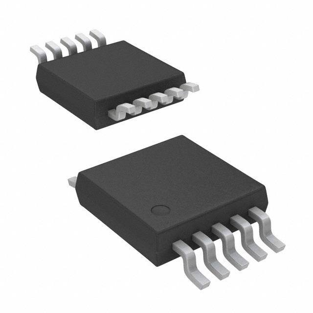
| 描述 | IC TX FRACT-N PLL 10TSSOP |
| 产品分类 | |
| 品牌 | Atmel |
| 数据手册 | |
| 产品图片 |
|
| 产品型号 | ATA5749C-6DQY-64 |
| rohs | 无铅 / 符合限制有害物质指令(RoHS)规范要求 |
| 产品系列 | - |
| 其它名称 | ATA5749C-6DQY-64DKR |
| 功率-输出 | 12.5dBm |
| 包装 | Digi-Reel® |
| 天线连接器 | PCB,表面贴装 |
| 存储容量 | - |
| 封装/外壳 | 10-TFSOP,10-MSOP(0.118",3.00mm 宽) |
| 工作温度 | -40°C ~ 125°C |
| 应用 | 通用数据传输 |
| 数据接口 | PCB,表面贴装 |
| 数据速率(最大值) | 40 kbps |
| 标准包装 | 1 |
| 特性 | - |
| 电压-电源 | 1.9 V ~ 3.6 V |
| 电流-传输 | 8.8mA |
| 调制或协议 | ASK,FSK |
| 频率 | 300MHz ~ 450MHz |


- 商务部:美国ITC正式对集成电路等产品启动337调查
- 曝三星4nm工艺存在良率问题 高通将骁龙8 Gen1或转产台积电
- 太阳诱电将投资9.5亿元在常州建新厂生产MLCC 预计2023年完工
- 英特尔发布欧洲新工厂建设计划 深化IDM 2.0 战略
- 台积电先进制程称霸业界 有大客户加持明年业绩稳了
- 达到5530亿美元!SIA预计今年全球半导体销售额将创下新高
- 英特尔拟将自动驾驶子公司Mobileye上市 估值或超500亿美元
- 三星加码芯片和SET,合并消费电子和移动部门,撤换高东真等 CEO
- 三星电子宣布重大人事变动 还合并消费电子和移动部门
- 海关总署:前11个月进口集成电路产品价值2.52万亿元 增长14.8%


PDF Datasheet 数据手册内容提取
ATA5749/ATA5749C Fractional-N PLL Transmitter IC DATASHEET Features ● Fully integrated fractional-N PLL ● ASK and closed loop FSK modulation ● Output power up to +12.5dBm from 300MHz to 450MHz ● Current consumption is scaled by output power programming ● Fast crystal oscillator start-up time of typically 200µs ● Low current consumption of typically 7.3mA at 5.5dBm ● Only one 13.0000MHz crystal for 314.1MHz to 329.5MHz and 424.5MHz to 439.9MHz operation ● Single ended RF power amplifier output ● Many software programmable options using SPI ● Output power from –0.5dBm to +12.5dBm ● RF frequency from 300MHz to 450MHz with different crystals ● FSK deviation with 396Hz resolution ● CLK output frequency 3.25MHz or 1.625MHz ● Data rate up to 40kbit/s (Manchester) ● 4KV HBM ESD protection including XTO ● Operating temperature range of –40°C to +125°C ● Supply voltage range of 1.9V to 3.6V ● TSSOP10 package Benefits ● Robust crystal oscillator with fast start up and high reliability ● Lower inventory costs and reduced part number proliferation ● Longer battery lifetime ● Supports multi-channel operation ● Wide tolerance crystal possible with PLL software compensation 9128J-RKE-07/15
1. Description The Atmel® ATA5749 is a fractional-N-PLL transmitter IC for 300MHz to 450MHz operation and is especially targeted for tire pressure sensor gauges, remote keyless entry, and passive entry and other automotive applications. It operates at data rates up to 40kbit/s Manchester for ASK and FSK with a typical 5.5dBm output power at 7.3mA. Transmitter parameters such as output power, output frequency, FSK deviation, and current consumption can be programmed using the SPI interface. This fully integrated PLL transmitter IC simplifies RF board design and results in very low material costs. Figure 1-1. Block Diagram Atmel ATA5749 CLK 1 CLK_DRV XTO_RDY Power 10 EN up/down 1 XTO Signal 4 or 8 Fractional-N-PLL CLK_ON DIV_CNTRL FSK_mod SDIN_TXDIN 2 9 GND FREQ[0:14] FSEP[0:7] Frac. Div. Digital Control and 433_N315 SCK 3 Registers ASK_mod PFD 8 VS PWR[0:3] CP ANT2 4 7 XTO1 LP XTO (FOX) ANT1 5 PA 6 XTO2 VCO 2 ATA5749/ATA5749C [DATASHEET] 9128J–RKE–07/15
2. Pin Configuration Figure 2-1. TSSOP10 Package Pinout CLK 1 10 EN SDIN_TXDIN 2 9 GND Atmel ATA5749 SCK 3 8 VS ANT2 4 7 XTO1 ANT1 5 6 XTO2 Table 2-1. Pin Description Pin Symbol Function 1 CLK CLK output 2 SDIN_TXDIN Serial bus data input and TX data input 3 SCK Serial bus clock input 4 ANT2 Antenna interface 5 ANT1 Antenna interface 6 XTO2 Crystal/C connection LOAD2 7 XTO1 Crystal/C connection LOAD1 8 VS Supply input 9 GND Supply GND 10 EN Enable input ATA5749/ATA5749C [DATASHEET] 3 9128J–RKE–07/15
3. Functional Description 3.1 Fractional-N PLL The Atmel® ATA5749 block diagram is shown in Figure 1-1 on page 2. The operation of the PLL is determined by the contents of a 32-bit configuration register. The 15-bit value FREQ is used with the 1-bit 434_N315 flag to determine the RF carrier frequency. This results in a user-selectable frequency step size of 793Hz (with 13.000MHz crystal). With this level of resolution, it is possible to compensate for crystal tolerance by adjusting the value of FREQ accordingly. This enables the use of lower cost crystals without compromising final accuracy. In addition, software programming of RF carrier frequency allows this device to be used in some multi-channel applications. Modulation type is selected with the 1-bit ASK_NFSK flag. FSK modulation is achieved by modifying the divider block in the feedback loop. The benefit to this approach is that performance- reducing RF spurs (common in applications that create FSK by “pulling” the load capacitance in the crystal oscillator circuit) are completely eliminated. The 8-bit value FSEP establishes the FSK frequency deviation. It is possible to obtain FSK frequency deviations from ±396Hz to ±101kHz in steps of ±396Hz. The PLL lock time is 1280/(external crystal frequency) and amounts to 98.46µs when using a 13.0000MHz crystal. When added to the crystal oscillator start-up time, a very fast time-to-transmit is possible (typically 300µs). This feature extends battery life in applications like Tire Pressure Monitoring Systems, where the message length is often shorter than 10ms and the time “wasted” during start-up and settling time becomes more significant. 3.2 Selecting the RF Carrier Frequency The fractional divider can be programmed to generate an RF output frequency f according to the formulas shown in RF Table 3-1. Note that in the case of f , the FSEP/2 value is rounded down to the next integer value if FSEP is an odd RFASK number. Table 3-1. RF Output Parameter Formulas RF Output Parameter S434_N315 = LOW S434_N315 = HIGH f (24+(FREQ+0.5)/16384)f (32.5+(FREQ+0.5)/16384)f RF_FSK_LOW XTO XTO f (24+(FREQ+FSEP+0.5)/16384) f (32.5+(FREQ+FSEP+0.5)/16384) f RF_FSK_HIGH XTO XTO f FSEP/32768f FSEP/32768f DEV__FSK XTO XTO f (24+(FREQ+FSEP/2+0.5)/16384) f (32.5+(FREQ+FSEP/2+0.5)/16384) f RF ASK XTO XTO FSEP can take on the values of 1 to 255. Using a 13.000MHz crystal, the range of frequency deviation f is DEV_FSK programmable from ±396Hz to ±101.16kHz in steps of ±396Hz. For example, with FSEP=100 the output frequency is FSK modulated with f = ±39.6kHz. DEV_FSK FREQ can take values in the range of values 2500 and 22000. Using a 13.0000MHz crystal, the output frequency f can be RF programmed to 315MHz by setting FREQ[0:14]=3730, FSEP[0:7]=100 and S434_N315=0. By setting FREQ[0:14]=14342, FSEP[0:7]=100 and S434_N315=1, 433.92MHz can be realized. 4 ATA5749/ATA5749C [DATASHEET] 9128J–RKE–07/15
The PA is enabled when the PLL is locked and the configuration register programming is completed. Upon enabling PA at FSK-mode, the RF output power will be switched on. At ASK mode, the input signal must be additionally set high for RF at output pins. The output power is user programmable from –0.5dBm to +12.5dBm in steps of approximately 1dB. Changing the output power requirements, you also modify the current consumption. This gives the user the option to optimize system performance (RF link budget versus battery life). The PA is implemented as a Class-C amplifier, which uses an open- collector output to deliver a current pulse that is nearly independent from supply voltage and temperature. The working principle is shown in Figure 3-1. Figure 3-1. Class C Power Amplifier Output V ANT1 V S I ANT2 I = (PWR[0:3]) Pulse V S V ANT1 L1 Power Meter C2 ANT1 5 I ANT2 50Ω Z LOPT ANT2 4 The peak value of this current pulse I is calibrated during Atmel® ATA5749 production to about ±20%, which Pulse corresponds to about 1.5dB variation in output power for a given power setting under typical conditions. The actual value of I can be programmed with the 4-bit value in PWR. This allows the user to scale both the output power and current Pulse consumption to optimal levels. ASK modulation is achieved by using the SDIN_TXDIN signal where a HIGH on this pin corresponds to RF carrier “ON” and a LOW corresponds to RF “OFF”. FSK uses the same signal path but HIGH switch on the upper FSK-frequency. ATA5749/ATA5749C [DATASHEET] 5 9128J–RKE–07/15
3.3 Crystal Oscillator The crystal oscillator (XTO) is an amplitude-regulated Pierce oscillator. It has fixed function and is not programmable. The oscillator is enabled when the EN is “set”. After the oscillator’s output amplitude reaches an acceptable level, the XTO_RDY flag is “set”. The CLK-pin becomes active if CLK_ON is set. The PLL receives its reference frequency. Typically, this process takes about 200µs when using a small sized crystal with a motional capacitance of 4fF. This start-up time strongly depends on the motional capacitance of the crystal and is lower with higher motional capacitance. The high negative starting impedance of R > 1500 is important to minimize the failure rate due to the “sleeping XTO12_START crystal” phenomena (more common among very small sized 3.2mm2.5mm crystals). 3.4 Clock Driver The clock driver block shown in Figure 1-1 on page 2 is programmed using the CLK_ONLY, CLK_ON, and DIV_CNTRL bits in the configuration register. When CLK_ONLY is “clear”, normal operation is selected and the fractional-N PLL is operating. When CLK_ON is “set”, the CLK output is enabled. The crystal clock divider ratio can be set to divide by four when DIV_CNTRL is “set” and divide by eight when DIV_CNTRL is “clear”. With a 13.0000MHz crystal, this yields an output of 3.25MHz or 1.625MHz, respectively. When CLK_ON is “clear”, no clock is available at CLK and the transmitter has less current consumption. The CLK signal can be used to clock a microcontroller. It is CMOS compatible and can drive up to 20pF of load capacitance at 1.625MHz and up to 10pF at 3.25MHz. When the device is in power-down mode, the CLK output stays low. Upon power up, CLK output remains low until the amplitude detector of the crystal oscillator detects sufficient amplitude and XTO_RDY and CLK_ON are “set”. After this takes place, CLK output becomes active. The CLK output is synchronized with the XTO_RDY signal so that the first period of the CLK output is always a full period (no CLK output spike at activation). To lower overall current consumption, it is possible to power down the entire chip except for the crystal oscillator block. This can be achieved when the CLK_ONLY is “set”. 6 ATA5749/ATA5749C [DATASHEET] 9128J–RKE–07/15
4. Application 4.1 Typical Application Figure 4-1. Typical Application Circuit IO1 Atmel ATA5749 CLK CLK 1 CLK_DRV XTO_RDY Power 10 EN Micro- up/down controller 1 XTO Signal 4 or 8 IO2 Fractional-N-PLL CLK_ON DIV_CNTRL FSK_mod IO3 2 9 GND FREQ[0:14] SDIN_TXDIN FSEP[0:7] Frac. Div. Digital C6 Control and 433_N315 SCK 3 Registers ASK_mod PFD 8 VS PWR[0:3] VS CP C3 C4 ANT2 4 7 XTO1 Loop antenna LP XTAL XTO (FOX) ANT1 5 PA 6 XTO2 VCO C5 C2 L1 C1 VS Figure 4-1 shows the typical application circuit. For C6, the supply-voltage blocking capacitor, value of 68nF X7R is recommended. C2 and C3 are NPO capacitors used to match the loop antenna impedance to the power amplifier optimum load impedance. They are based on the PCB trace antenna and are ≤ 20pF NPO capacitors. C1 (typically 1nF X7R) is needed for the supply blocking of the PA. In combination with L1 (200nHto300nH), they prevent the power amplifier from coupling to the supply voltage and disturbing PLL operation. They should be placed close to pin5. L1 also provides a low resistive path to V to deliver the DC current to ANT1. S ATA5749/ATA5749C [DATASHEET] 7 9128J–RKE–07/15
The PCB loop antenna should not exceed a trace width of 1.5mm otherwise the Q-factor of the loop antenna is too high. C4 and C5 should be selected so that the XTO runs on the load resonance frequency of the crystal. A crystal with a load capacitance of 9pF is recommended for proper start-up behavior and low current consumption. When determining values for C4 and C5, a parasitic capacitance of 3pF should be included. With value of 15pF for C4 and C5, an effective load capacitance of 9pF can be achieved, e.g., 9pF=(15pF+3pF)/2. The supply V is typically delivered from a single Li-Cell. S 4.1.1 Antenna Impedance Matching The maximum output power is achieved by using load impedances according to Table 4-1 on page 9 and Table 4-2 on page 9 and the output power. The load impedance Z is defined as the impedance seen from the Atmel® LOPT ATA5749 ANT1, ANT2 into the matching network. This is not the output impedance of the IC but essentially the peak voltage divided by the peak current with some additional parasitic effects (Cpar). Table 4-1 on page 9 and Table 4-2 on page 9 do not contain information pertaining to C3 in Figure 4-2, which is an option for better matching at low power steps. Figure 4-2 is the circuit that was used to obtain the typical output power measurements in Figure 4-3 on page 10 and typical current consumption in Figure 4-4 on page 10. Table 4-1 and Table 4-2 on page 9 provide recommended values and performance info at various output power levels. For reference, Z is defined as the impedance seen from the Atmel LOPT ATA5749 ANT1, ANT2 into the matching network. Figure 4-2. Output Power Measurement Circuit ZLOPT ANT2 4 Power Meter C2 ANT1 PA 5 50Ω C3 L1 C1 VS 8 ATA5749/ATA5749C [DATASHEET] 9128J–RKE–07/15
The used parts at Table 4-1 and Table 4-2 are: Inductors: high Q COILCRAFT 0805CS; Capacitors: AVX ACCU-P 0402 Table 4-1. Measured PA Matching at 315MHz (CLK_ON=“LOW”) at Typ. Samples PWR Desired L1 C2 C3 1) R Z Cpar Actual Power LOPT LOPT Register Power(dBm) (nH) (pF) (pF) () () (pF) (dBm) 3 –0.5 110 1.2 1.6 2950 110+540j 0.9 –0.37 4 1.0 100 1.5 --- 1940 150+520j 0.9 1.12 5 2.5 100 1.5 --- 1550 190+520j 0.9 2.11 6 3.5 100 1.5 --- 1250 220+480j 0.9 3.23 7 4.5 82 1.8 --- 1000 240+430j 0.9 4.38 8 5.5 82 2.2 --- 730 280+360j 0.9 5.42 9 6.5 68 2.7 --- 580 290+300j 0.9 7.14 10 7.5 68 2.7 --- 460 290+290j 0.9 8.22 11 8.5 68 3.3 --- 350 280+225j 0.9 8.63 12 9.5 56 3.6 --- 320 250+150j 0.9 9.79 13 10.5 47 4.7 --- 250 215+85j 0.9 10.52 14 11.5 47 5.6 --- 190 180+50j 0.9 11.67 15 12.5 47 5.6 --- 160 160+45j 0.9 13 Note: 1. Leave capacitor out at row without value Table 4-2. Measured PA Matching at 433.92MHz (CLK_ON=“LOW”) at Typ. Samples PWR Desired L1 C2 C3 1) R Z Cpar Actual Power LOPT LOPT Register Power(dBm) (nH) (pF) (pF) () () (pF) (dBm) 3 –0.5 68 0,9 1.5 2800 60+400j 0.9 –0.62 4 1.0 56 2.7 + 2.2 --- 1850 90+390j 0.9 1.3 5 2.5 56 1.2 --- 1450 110+380j 0.9 2.73 6 3.5 47 1.8 5.6 1150 130+370j 0.9 3.03 7 4.5 47 1.6 --- 950 150+350j 0.9 4.63 8 5.5 47 1.8 --- 680 180+300j 0.9 6.18 9 6.5 43 2.2 1 560 200+270j 0.9 6.66 10 7.5 36 2.4 --- 450 210+230j 0.9 7.91 11 8.5 33 3 --- 340 200+170j 0.9 8.68 12 9.5 36 2.7 --- 310 195+150j 0.9 9.8 13 10.5 36 3.6 --- 230 175+100j 0.9 10.49 14 11.5 27 4.7 --- 180 150+70j 0.9 11.6 15 12.5 27 4.7 --- 150 130+50j 0.9 12.5 Note: 1. Leave capacitor out at row without value ATA5749/ATA5749C [DATASHEET] 9 9128J–RKE–07/15
Figure 4-3. Typical Measured Output Power 15 V = 3.6V, PWR[0:15] = 15] 315MHz S 433MHz 13 V = 3.0V, PWR[0:15] = 15 11 S m] B 9 d VS = 1.9V, PWR[0:15] = 15 s [ a 7 e V = 3.6V, PWR[0:15] = 8 m S P 5 V = 3.0V, PWR[0:15] = 8 S 3 V = 1.9V, PWR[0:15] = 8 S 1 -40 27 85 125 Temperature [°C] Figure 4-4. Typical Current Consumption I at Port VS 23 315MHz 21 VS = 3.6V, PWR[0:15] = 15 433MHz 19 V = 3.0V, PWR[0:15] = 15 17 S V = 1.9V, PWR[0:15] = 15 S A] 15 m s [ 13 v I 11 V = 3.6V, PWR[0:15] = 8 9 S V = 3.0V, PWR[0:15] = 8 S 7 V = 1.9V, PWR[0:15] = 8 5 S -40 27 85 125 Temperature [˚C] 10 ATA5749/ATA5749C [DATASHEET] 9128J–RKE–07/15
5. Pulling of Frequency due to ASK Modulation (PA Switching) The switching effect on VCO frequency in ASK Mode is very low if a correct PCB layout and decoupling is used. Therefore, power ramping is not needed to achieve a clean spectrum (see Figure 5-1). Figure 5-1. Typical RF Spectrum of 40kHz ASK Modulation at Pout = 12.5dBm ATA5749/ATA5749C [DATASHEET] 11 9128J–RKE–07/15
6. Configuration Register 6.1 General Description The user must program all 32bits of the configuration register upon power up (EN=HIGH) or whenever changes to operating parameters are desired. The configuration register bit assignments and descriptions can be found in Table 6-1 and Table 6-2. Table 6-1. Organization of the Control Register MSB 31 30 29 28 27 26 25 24 23 22 21 20 19 18 17 16 CLK_ S434_ FREQ FREQ FREQ FREQ FREQ FREQ FREQ FREQ FREQ FREQ FREQ FREQ FREQ FREQ ONLY N315 [14] [13] [12] [11] [10] [9] [8] [7] [6] [5] [4] [3] [2] [1] Frequency Adjust = FREQ[0..14] FREQ[0] + 2 FREQ[1] + 4 FREQ[2] + ... + FREQ[14] 16384 = 0..32767 LSB 15 14 13 12 11 10 9 8 7 6 5 4 3 2 1 0 FREQ FSEP FSEP FSEP FSEP FSEP FSEP FSEP FSEP DIV_ PWR PWR PWR PWR ASK_ CLK_ [0] [7] [6] [5] [4] [3] [2] [1] [0] CNTRL [3] [2] [1] [0] NFSK ON Output Power = PWR[0..3] FSK Shift = FSEP[0..7] PWR[0] + .. + PWR[3] 8 = FSEP[0] + ... + FSEP[7] 128 = 0..255 0..15 Table 6-2. Control Register Functional Descriptions Name Bit No. Size Remarks Activates/deactivates CLK_ONLY mode CLK_ONLY 31 1 Low = Normal mode High = Clock only mode (Figure 4-1 on page 7) VCO band selection S434_N315 30 1 High = 367MHz to 450MHz Low = 300MHz to 368MHz PLL frequency adjust FREQ[0:14] 15 ... 29 15 See Table 6-1 for formula FSK deviation adjust FSEP[0:7] 7 ... 14 8 See Table 6-1 for formula CLK output divider ratio DIV_CNTRL 6 1 Low = f /8 XTO High = f /4 XTO PA output power adjustment PWR[0:3] 2 ... 5 4 See Table 4-1 and Table 4-2 on page 9 Modulation type ASK_NFSK 1 1 Low = FSK High = ASK CLK_DRV port control CLK_ON 0 1 HIGH = CLK port is ON LOW = CLK port is OFF 12 ATA5749/ATA5749C [DATASHEET] 9128J–RKE–07/15
6.2 Programming The configuration register is programmed serially using the SPI bus, starting with the MSB. It consists of the Enable line (EN), the Data line (SDIN_TXDIN), and the SPI-Bus Clock (SCK). The SDIN_TXDIN data is loaded on the positive edge of the SCK. The contents of the configuration register become programmed on the negative SCK edge of the last bit (LSB) of the programming sequence. The timing of this bus is shown in Figure 6-1. Note that the maximum usable clock speed on the SPI bus is limited to 2MHz. Figure 6-1. SPI Bus Timing EN T SCK_High TEN_setup TSCK_Cycle TSDIN_TXDIN_setup T SCK_Low SCK T T Hold Setup SDIN_TXDIN MSB X MSB-1 X At the conclusion of the 32 bit programming sequence, the SDIN_TXDIN line becomes the modulation input for the RF transmitter. After programming is complete, the SCK signal has no effect on the device. To disable the transmitter and enter the OFF Mode, EN and SDIN_TXDIN must be returned to the LOW state. For clarity, several additional timing diagrams are included. Figure 6-2 shows the situation when the programming terminates faster then the XTO is ready. Figure 6-2. Timing Diagram if Register Programming is Faster than T XTO ΔT XTO EN (Input) SDIN_TXDIN (Input) 32-bit Configuration TX-Data SCK (Input) X X X T PLL CLK (Output) PA (Output Power) FSK; TX_Mode2 OFF_ Start_Up_ Start_Up_ TX_ OFF_Mode ASK: Mode Mode_1 Mode_2 Mode1 TX_Mode1 and TX_Mode2 ATA5749/ATA5749C [DATASHEET] 13 9128J–RKE–07/15
Figure 6-3 shows the combination with slow programming and a faster ramp up of XTO. A diagram of the operating modes is shown in Figure 6-5 on page 16 and a description of which circuit blocks are active is provided in Table 6-3 on page 15. This also contains the information needed for the calculation of consumed charge for one operation cycle. Figure 6-3. Timing Diagram if Programming is Slower than T XTO ΔT XTO EN (Input) T PLL SDIN_TXDIN (Input) 32-bit Configuration TX-Data SCK (Input) X X CLK (Output) PA (Output Power) FSK; TX_Mode2 OFF_ Start_Up_ Start_Up_ TX_ OFF_Mode ASK: Mode Mode_1 Mode_2 Mode1 TX_Mode1 and TX_Mode2 6.3 Reprogramming without Stopping the Crystal Oscillator After the configuration register is programmed and RF data transmission is completed, the OFF mode is normally entered. This stops the crystal oscillator and PLL. If it is desirable to modify the contents of the configuration register without entering the OFF mode, the Reset_Register_Mode can be used. To enter the Reset_Register_Mode, the SDIN_TXDIN must be asserted HIGH while the EN is asserted LOW for at least 10µs Reset_min time. This state is shown in Figure 6-4 on page 15, State Diagram of Operating Modes. In Reset_Register_Mode, the PA and fractional PLL remain OFF but the XTO remains active. This state must stay forminimum 10µs. At the next step you must rise first EN and SDIN_TXDIN 10µs delayed. While in this mode, the 32bit configuration register data can be sent on the SPI bus as shown in Figure 6-2 on page 13. After data transmission, the device can be switched back to OFF_Mode by asserting EN, SCK, and SDIN_TXDIN to a LOW state. An example of programming from the Reset_Register_Mode is shown in Figure 6-4 on page 15. 14 ATA5749/ATA5749C [DATASHEET] 9128J–RKE–07/15
Figure 6-4. Timing Diagram when using Reset_Register_Mode T EN_Reset EN (Input) TPLL TPLL TSDIN_TXDIN_setup TEN_setup SDIN_TXDIN (Input) 32-bit TX_ 32-bit TX_ Configuration Data Configuration Data SCK (Input) CLK (Output) PA (Output Power) FSK; FSK; TX_Mode2 TX_Mode2 Start_Up_ Start_Up_ Reset_ Con- Con- OFF_ ASK: ASK: Mode_1 Mode_2 Register_ figuration_ figuration_ Mode TX_Mode1 and TX_Mode1 and Mode Mode_1 Mode_2 TX_Mode2 TX_Mode2 TX_Mode1 TX_Mode1 Table 6-3. Active Circuits as a Function of Operating Mode Operating Mode Active Circuit Blocks OFF_Mode -none- Start_Up_Mode_1 Power up/down; XTO; digital control Start_Up_Mode_2 Power up/down; XTO; digital control; fractional-N-PLL TX_Mode1 Power up/down; XTO; digital control; fractional-N-PLL; CLK_DRV(1) TX_Mode2 Power up/down; XTO; digital control; fractional-N-PLL; CLK_DRV(1); PA Clock_Only_Mode Power up/down; XTO; digital control; CLK_DRV(1) Reset_Register_Mode Power up/down; XTO; digital control; CLK_DRV(1) Configuration_Mode_1 Power up/down; XTO; digital control; CLK_DRV(1) Configuration_Mode_2 Power up/down; XTO; digital control; CLK_DRV(1); fractional-N-PLL Note: 1. Only if activated with CLK_ON=HIGH ATA5749/ATA5749C [DATASHEET] 15 9128J–RKE–07/15
Figure 6-5. State Diagram of Operating Modes OFF_Mode EN = 'High' EN = 'Low' SDIN_TXDIN = 'Low' SDIN_TXDIN = 'Low' EN = 'Low' EN = 'Low' Start-Up_Mode_1 EN = 'Low' SDIN_TXDIN = 'Low' SDIN_TXDIN = 'Low' SDIN_TXDIN = 'Low' CLK_Only = 'Low' CLK_Only = 'High' register parity programmed1 register programmed2 XTO_RDY = 'High' CLK_Only = 'Low' register programmed2 ASK_NFSK = 'Low' or XTO_RDY = 'High' Start-Up_Mode_2 (ASK_NFSK = 'High' and SDIN_TXDIN = 'High') PLL locked3 TX_Mode_2 TX_Mode_1 Clock_only_Mode CLK_Only = 'Low' ASK_NFSK = 'High' and register programmed2 CLK_Only = 'High' SDIN_TXDIN = 'Low' register programmed2 Configuration_Mode_2 CLK_Only = 'Low' register parity programmed1 EN = 'Low' EN = 'Low' EN = 'Low' SDIN_TXDIN = 'High' SDIN_TXDIN = 'High' SDIN_TXDIN = 'High' Configuration_Mode_1 1)"register partly programmed": negative SCK edge of 32-bit register programming MSB-1 EN = 'High' (S433_N315) SDIN_TXDIN = 'Low' 2) "register programmed'" negative SCK edge of 32-bit register programming LSB (CLK_ON) Reset_Register_Mode 3) "PLL locked" 1280 XTO cycles (TPLL) after register programmed and XTO_RDY = 'High' To transition from one state to another, only the conditions next to the transition arrows must be fulfilled. No additional settings are required. 16 ATA5749/ATA5749C [DATASHEET] 9128J–RKE–07/15
7. ESD Protection Circuit Figure 7-1. ESD Protection Circuit VS ANT1 CLK SCK EN ANT2 XTO2 XTO1 SDIN_TXDIN GND 8. Absolute Maximum Ratings Stresses beyond those listed under “Absolute Maximum Ratings” may cause permanent damage to the device. This is a stress rating only and functional operation of the device at these or any other conditions beyond those indicated in the operational sections of this specification is not implied. Exposure to absolute maximum rating conditions for extended periods may affect device reliability. Parameters Symbol Min. Max. Unit Supply voltage V –0.3 +4.0 V S Power dissipation P 100 mW tot Junction temperature T 150 °C j Storage temperature T –55 +125 °C stg Ambient temperature Tamb1 –40 +125 °C Ambient temperature in power-down mode for 30 minutes without damage with V ≤3.2V, V <0.25V Tamb2 175 °C S ENABLE or ENABLE is open, V <0.25V, V <0.25V ASK FSK ESD (Human Body Model ESD S5.1) every pin HBM –4 +4 kV excluding pin5 (ANT1) ESD (Human Body Model ESD S5.1) for pin5 (ANT1) HBM –2 +2 kV ESD (Machine Model JEDEC A115A) every pin MM –200 +200 V excluding pin5 (ANT1) ESD (Machine Model JEDEC A115A) for pin5 (ANT1) MM –150 +150 V ESD – STM 5.3.1-1999 every pin CDM 750 V 9. Thermal Resistance Parameters Symbol Value Unit Thermal resistance, junction ambient R 170 K/W thJA ATA5749/ATA5749C [DATASHEET] 17 9128J–RKE–07/15
10. Electrical Characteristics V = 1.9V to 3.6V T = –40°C to +125°C, CLK_ON = “High”; DIV_CNTRL = “Low”, CLOAD_CLK = 10pF. f =13.0000MHz, S amb XTO f =1.625MHz unless otherwise specified. If crystal parameters are important values correspond to a crystal with C =4.0fF, CLK M C =1.5pF, C =9pF and R ≤ 170. Typical values are given at V =3.0V and T =25°C 0 LOAD M S amb No. Parameters Test Conditions Pin Symbol Min. Typ. Max. Unit Type* 1 Current consumption V(SDIN_TXDIN,SCK,EN)=Low Supply current, 1.1 T ≤ +25°C 5, 8 I 1 100 nA OFF_mode amb S_Off_Mode A T ≤ +85°C 20 350 nA amb T ≤ +125°C 265 7,000 nA amb Supply current, 1.2 V ≤ 3.0V 5, 8 I 3.6 4.75 mA B TX_mode1 S S_TX_Mode1 Supply current, V ≤ 3.0V 1.3 S 5, 8 I 7.3 8.8 mA B TX_mode2 PWR[0:3] = 8 (5.5dBm) S_TX_Mode2 Supply current, I 1.4 V ≤ 3.0V 5, 8 S_CLK_Only _ 480 680 µA B CLK_only_mode S Mode V ≤ 3.0V S CLK_ON = “Low” Supply current I = I + I S S_any_Mode CLKoff1 1.5 reduction, clock driver 5, 8 I –250 –300 µA B CLKoff1 (can be applied to all modes off except off_mode, add typ. to typ. and max. to max. values) V ≤ 3.0V S DIV_CNTRL = “High” Supply current fCLK=3.24MHz 1.6 increase, clock driver IS= IS_any__Mode + ICLKhigh 5, 8 ICLKhigh 150 190 µA B higher frequency (can be applied to all modes except off_mode add typ. to typ. and max. to max. values) I S_Reset_ Reset_register_mode / 1.7 V ≤ 3.0V 5, 8 Register_Mode / 680 µA B Configuration_mode_1 S I S_Configuration _ Mode_1 I S_Configuration Configuration_mode_2 / / 1.8 V ≤ 3.0V 5, 8 _Mode_2 4.75 mA B Start_up_mode_2 S I S_Start_Up _Mode_2 I 1.9 Start_up_mode_1 V ≤ 3.0V 5, 8 S_Start_Up 350 µA B S _Mode_1 2 Power amplifier (PA) V = 3.0V, T = 25°C S amb PWR[0:3] = 4 Output power 1, 2.1 Z = Z according to (5) P –1.0 +1.0 +3.0 dBm B TX_mode2 LOAD LOPT OUT_1 Table 4-1 on page 9 and Table 4-2 on page 9 *) Type means: A = 100% tested, B = 100% correlation tested, C = Characterized on samples, D = Design parameter Note: (Pin Number) in brackets mean they are measured matched to 50 according to Figure 4-2 on page 8 with component values and optimum load impedances according to Table 4-1 and Table 4-2 on page 9 18 ATA5749/ATA5749C [DATASHEET] 9128J–RKE–07/15
10. Electrical Characteristics (Continued) V = 1.9V to 3.6V T = –40°C to +125°C, CLK_ON = “High”; DIV_CNTRL = “Low”, CLOAD_CLK = 10pF. f =13.0000MHz, S amb XTO f =1.625MHz unless otherwise specified. If crystal parameters are important values correspond to a crystal with C =4.0fF, CLK M C =1.5pF, C =9pF and R ≤ 170. Typical values are given at V =3.0V and T =25°C 0 LOAD M S amb No. Parameters Test Conditions Pin Symbol Min. Typ. Max. Unit Type* V = 3.0V S 5, 8 I 5.4 6.7 mA B Supply current 1, PWR[0:3] = 4 S_P1 2.2 TX_mode2 V = 3.6V S 5, 8 I 7.0 mA A PWR[0:3] = 4 S_P1 V = 3.0V, T = 25°C S amb PWR[0:3] = 8 Output power 2, 2.3 Z = Z according to (5) P 4.0 5.5 7.0 dBm A TX_mode2 LOAD LOPT OUT_2 Table 4-1 on page 9 and Table 4-2 on page 9 V = 3.0V, PWR[0:3] = 8 S 5, 8 I 7.3 8.8 mA B Supply current 2, [typ. 5.5dBm; see 2.3] S_P2 2.4 TX_mode2 V = 3.6V, PWR[0:3] = 8 S 5, 8 I 9.1 mA A [typ. 5.5dBm; see 2.3] S_P2 V = 3.0V, T = 25°C S amb PWR[0:3] = 15 Output power 3, 2.5 Z = Z according to (5) P 11.0 12.5 14.0 dBm B TX_mode2 LOAD LOPT OUT_3 Table 4-1 on page 9 and Table 4-2 on page 9 V = 3.0V S 5, 8 I 20.2 23.5 mA A Supply current 3, PWR[0:3] = 15 S_P3 2.6 TX_mode2 V = 3.6V S 5, 8 I 24.5 mA A PWR[0:3] = 15 S_P3 T = –40°C to +125°C amb Output power variation VS = 1.9V to 3.6V 2.7 for full temperature and Pout=POUT_x+POUT (5) POUT –4.0 +1.5 dB B supply voltage range (can be applied to all power levels) 3 Crystal oscillator (XTO) Maximum series 3.1 resistance R of XTAL C < 2.0pF 6, 7 R 170 D M 0 M_MAX after start-up Motional capacitance of 3.2 Recommended values 6, 7 C 2 4.0 15 fF D XTAL M C < 2.0pF 0 C = 4.0fF M Stabilized Amplitude R = 20 3.3 M 6, 7 mVpp A XTAL C = 9pF LOAD V(XTO2) – V(XTO1) Vpp 640 XTO21 V(XTO1) Vpp 320 XTO1 1.0 < C < 2.0pF 0 Pulling of f versus R < 170 XTO M 3.4 temperature and supply C = 9pF 6, 7 f –3 +3 ppm C LOAD RF change 4fF < C < 10fF M C < 15fF –5 +5 M *) Type means: A = 100% tested, B = 100% correlation tested, C = Characterized on samples, D = Design parameter Note: (Pin Number) in brackets mean they are measured matched to 50 according to Figure 4-2 on page 8 with component values and optimum load impedances according to Table 4-1 and Table 4-2 on page 9 ATA5749/ATA5749C [DATASHEET] 19 9128J–RKE–07/15
10. Electrical Characteristics (Continued) V = 1.9V to 3.6V T = –40°C to +125°C, CLK_ON = “High”; DIV_CNTRL = “Low”, CLOAD_CLK = 10pF. f =13.0000MHz, S amb XTO f =1.625MHz unless otherwise specified. If crystal parameters are important values correspond to a crystal with C =4.0fF, CLK M C =1.5pF, C =9pF and R ≤ 170. Typical values are given at V =3.0V and T =25°C 0 LOAD M S amb No. Parameters Test Conditions Pin Symbol Min. Typ. Max. Unit Type* DC voltage after XTAL V(XTO2) – V(XTO1) 3.5 6, 7 V 40 mV C amplitude stable XTO running DC_XTO This value is important for crystal oscillator start-up behavior Negative real part of C < 2.0pF, –1,500 3.6 XTO impedance at 0 6, 7 R –2,200 B 8pF < C < 10pF XTO12_START begin of start-up LOAD F = 13.000MHz XTAL 11.0MHz<F <14.8MHz –1,300 XTAL Recommended values for proper start-up and low current consumption External capacitors Quality NPO C 3.7 6, 7 4 –5% 15 +5% pF D C4, C5 C = (C + C ) C LOAD 4 XTO1 5 (C + C ) / 5 XTO2 (C + C + C + C ) 4 5 XTO1 XTO2 C = 9pF (inc. PCB) Load_nom Pin capacitance The PCB capacitance of about C –15% 2 +15% 3.8 6, 7 XTO1 pF C XTO1 and XTO2 1pF has to be added C –15% 2 +15% XTO2 Time between EN = “High” and XTO_RDY = “High” Crystal oscillator start- C < 2.0pF, 4fF < C < 15fF 0.20 0.3 3.9 0 M 6, 7, 1 T ms B up time C < 2.0pF, 2fF < C < 15fF XTO 0.32 0.5 0 M R < 170 M 11.0MHz<F < 14.8MHz XTAL Maximum shunt Required for stable operation of 3.10 6, 7 C 1.5 3.0 pF D capacitance C of XTAL XTO, C > 7. 5pF 0_MAX 0 Load Oscillator frequency 433.92MHz and 315MHz other 13.0000 3.11 6, 7 f MHz C XTO frequencies XTO 11.0 14.8 4 Fractional-N-PLL Frequency range of RF S434_N315 = “LOW” 300 368 4.1 5 f MHz A frequency S434_N315 = “HIGH” RF 367 450 Time between XTO_RDY=“High” and Register 98.46 µs B 4.2 Locking time of the PLL programmed till PLL is locked 1, 5 T PLL 1280/ f =13.0000MHz oXtThOer f fXTO XTO Unity gain loop frequency of 4.3 PLL loop bandwidth 5 f 140 280 380 kHz B synthesizer Loop_PLL 4.4 In loop phase noise PLL25kHz distance to carrier 5 L –83 –76 dBc/Hz A PLL Out of loop phase noise At 1MHz L –91 –84 dBc/Hz A 4.5 5 at1M (VCO) At 36MHz Lat36M –122 –115 dBc/Hz C Duty cycle of the modulation FSK modulation signal = 50%, (this corresponds 4.6 2, 5 F 0 40 kHz B frequency to 40kBit/s Manchester coding MOD_FSK and 80kBit/s NRZ coding) *) Type means: A = 100% tested, B = 100% correlation tested, C = Characterized on samples, D = Design parameter Note: (Pin Number) in brackets mean they are measured matched to 50 according to Figure 4-2 on page 8 with component values and optimum load impedances according to Table 4-1 and Table 4-2 on page 9 20 ATA5749/ATA5749C [DATASHEET] 9128J–RKE–07/15
10. Electrical Characteristics (Continued) V = 1.9V to 3.6V T = –40°C to +125°C, CLK_ON = “High”; DIV_CNTRL = “Low”, CLOAD_CLK = 10pF. f =13.0000MHz, S amb XTO f =1.625MHz unless otherwise specified. If crystal parameters are important values correspond to a crystal with C =4.0fF, CLK M C =1.5pF, C =9pF and R ≤ 170. Typical values are given at V =3.0V and T =25°C 0 LOAD M S amb No. Parameters Test Conditions Pin Symbol Min. Typ. Max. Unit Type* Duty cycle of the modulation ASK modulation signal = 50%, (this corresponds 4.7 2, 5 F 0 40 kHz B frequency to 40kBit/s Manchester coding MOD_ASK and 80kBit/s NRZ coding) At f ±f / 8 –47 RF XTO 4.8 Spurious emission At f ±f / 4 5 Spur –47 dBc B RF XTO At f ±f –60 RF XTO DIV_CNTRL = “High” 4.9 Spurious emission At f ± f / 4 5 Spur –47 dBc B RF XTO At f ± f –58 RF XTO CLK_ON = “Low” 4.10 Spurious emission 5 Spur dBc B At f ± f –60 0 XTO ASK_NFSK = “High” TX_Mode_2 FREQ[0:14]=3730, FSEP[0:7]=101 S434_N315 = “Low” f ±3.00MHz –50 4.11 Fractional spurious RF 5 Spur dBc B f ±6.00MHz –50 RF FREQ[0:14]=14342, FSEP[0:7]=101 S434_N315=“High” f ±3.159MHz –50 RF f ± 9.840MHz –50 RF ±0.396 ±101.16 kHz A f =13.0000MHz FSK frequency XTO 4.12 other f 5 f f / f / deviation XTO dev XTO XTO see Table 3-1 on page 4 32768 128.5 793 Hz A f = 13.0000MHz 4.13 Frequency resolution XTO f f / other f PLL XTO XTO 16384 *) Type means: A = 100% tested, B = 100% correlation tested, C = Characterized on samples, D = Design parameter Note: (Pin Number) in brackets mean they are measured matched to 50 according to Figure 4-2 on page 8 with component values and optimum load impedances according to Table 4-1 and Table 4-2 on page 9 ATA5749/ATA5749C [DATASHEET] 21 9128J–RKE–07/15
11. Timing Characteristics (Atmel ATA5749) V = 1.9V to 3.6V, T = –40°C to +125°C. Typical values are given at V = 3.0V and T = 25°C. All parameters are referred to GND S amb S amb (pin9). Parameters where crystal relevant parameters are important correspond to a crystal with C =4.0fF, C =1.5pF, C =9pF M 0 LOAD and R ≤ 170 unless otherwise specified. M No. Parameters Test Conditions Pin Symbol Min. Typ. Max. Unit Type* EN set-up time to rising 1.1 1, 10 T 10 µs C edge of SCK EN_setup SDIN_TXDIN set-up time T 1.2 2, 10 SDIN_TXDIN 125 ns C to falling edge of EN _setup SDIN_TXDIN set-up time 1.3 2, 3 T 10 ns C to rising edge of SCK Setup SDIN_TXDIN hold time 1.4 2, 3 T 10 ns C from rising edge of SCK Hold 1.5 SCK Cycle time 3 T 500 ns C SCK_Cycle 1.6 SCK high time period 3 T 200 ns C SCK_High 1.7 SCK low time period 3 T 200 ns C SCK_Low EN low time period with 1.8 SDIN_TXDIN=“High” 2, 10 T 10 us C EN_Reset for register reset f = 13.000MHz XTO Clock output frequency DIV_CNTRL=“High” 3.25 1.9 (CMOS microcontroller (f = f / 4) 1 f MHz A CLK XTO CLK compatible) DIV_CNTRL = “Low” 1.625 (f = f / 8) CLK XTO Cload ≤ 20pF, DIV_CNTRL = “Low” Clock output minimum (f =f / 8) 1.10 clk XTO 1 T 125 220 ns A “high” and “low” time “High” = 0.8 V , CLKLH S “Low” = 0.2 V , S f < 1.625MHz CLK Cload ≤ 10pF, DIV_CNTRL = “High” Clock output minimum (f = f / 4) 1.11 clk XTO 1 T 62.5 110 ns A “high” and “low” time “High” = 0.8 V , CLKLH S “Low” = 0.2 V , S f < 3.25MHz CLK Cload ≤ 20pF, DIV_CNTRL = “Low” Clock output minimum (f = f / 8) 1.12 clk XTO 1 T 125 180 ns C “high” and “low” time “High” = 0.8 V , CLKLH S “Low” = 0.2 V , S f < 1.85MHz CLK Cload ≤ 10pF, DIV_CNTRL=“High” Clock output minimum (f = f / 4) 1.13 clk XTO 1 T 62.6 90 ns C “high” and “low” time “High” = 0.8 V , CLKLH S “Low” = 0.2 V , S f < 3.7MHz CLK *) Type means: A = 100% tested, B = 100% correlation tested, C = Characterized on samples, D = Design parameter 22 ATA5749/ATA5749C [DATASHEET] 9128J–RKE–07/15
12. Digital Port Characteristics V = 1.9V to 3.6V, T = 40°C to +125°C unless otherwise specified. Typical values are given at V =3.0V and T =25°C, all inputs S amb S amb are Schmitt trigger interfaces. No. Parameters Test Conditions Pin Symbol Min. Typ. Max. Unit Type* “Low” level input voltage V 0 0.25 V II 1.1 SDIN_TXDIN “High” level input voltage V V –0.25 V V A ih S S Internal pull-down resistor R 160 250 380 k PDN “Low” level input voltage V 0 0.25 V II 1.2 SCK “High” level input voltage V V –0.25 V V A ih S S Internal pull-down resistor R 160 250 380 k PDN “Low” level input voltage V 0 0.23 V II 1.3 EN input “High” level input voltage V V –0.25 V V A ih S S Internal pull-down resistor R 160 250 380 k PDN *) Type means: A = 100% tested, B = 100% correlation tested, C = Characterized on samples, D = Design parameter ATA5749/ATA5749C [DATASHEET] 23 9128J–RKE–07/15
13. Ordering Information Extended Type Number Package Remarks ATA5749C-6DQY-64 TSSOP10 - 14. Package Information x 1 a 0. 3±0.1 3±0.1 m ± 5 1 8 1. 0. 0.25 5 1 0.5 nom. 3.8±0.3 0. 4 x 0.5 = 2 nom. 4.9±0.1 10 9 8 7 6 technical drawings according to DIN specifications Dimensions in mm 1 2 3 4 5 Not indicated tolerances ±0.05 09/16/05 TITLE GPC DRAWING NO. REV. Package Drawing Contact: Package: TSSOP packagedrawings@atmel.com (acc. to JEDEC Standard MO-187) 6.543-5095.01-4 3 24 ATA5749/ATA5749C [DATASHEET] 9128J–RKE–07/15
15. Revision History Please note that the following page numbers referred to in this section refer to the specific revision mentioned, not to this document. Revision No. History 9128J-RKE-07/15 Section 13 “Ordering Information” on page 24 updated 9128I-RKE-04/14 Put document in the latest template 9128H-RKE-08/11 Section 13 “Ordering Information” on page 24 updated ATA5749C on page 1 added 9128G-RKE-03/11 Section 13 “Ordering Information” on page 24 updated Page 9: Table 4-1 updated 9128F-RKE-09/10 Page 9: Table 4-2 updated El. Char. table: rows 1.2, 1.3, 1.4, 1.7, 1.8, 1.9, 2.1, 2.2, 2.4, 2.5 updated 9128E-RKE-09/10 Dig. Port Char. table: row 1.3 updated Ordering table updated Features on page 1 updated 9128D-RKE-01/09 Section 8 “Absolute Maximum Ratings” on page 17 updated Features on page 1 updated 9128C-RKE-10/08 Section 8 “Absolute Maximum Ratings” on page 17 updated Section 12 “Digital Port Characteristics” on page 23 updated Put document in the latest template Features on page 1 updated Section 1 “Description” on page 1 updated Figure 1-1 “Block Diagram” on page 2 updated Section 3.1 “Fractional-N PLL” on page 4 updated 9128B-RKE-08/08 Section 3.4 “Clock Driver” on page 6 updated Figure 4-1 “Typical Application Circuit” on page 7 updated Figure 4-2 “Output Power Measurement Circuit” on page 8 updated Section 10 “Electrical Characteristics” numbers 4.2, 4.12 and 4.13 on pages 20 to 21 updated ATA5749/ATA5749C [DATASHEET] 25 9128J–RKE–07/15
X X X X X X Atmel Corporation 1600 Technology Drive, San Jose, CA 95110 USA T: (+1)(408) 441.0311 F: (+1)(408) 436.4200 | www.atmel.com © 2015 Atmel Corporation. / Rev.: 9128J–RKE–07/15 Atmel®, Atmel logo and combinations thereof, Enabling Unlimited Possibilities®, and others are registered trademarks or trademarks of Atmel Corporation or its subsidiaries. Other terms and product names may be trademarks of others. DISCLAIMER: The information in this document is provided in connection with Atmel products. No license, express or implied, by estoppel or otherwise, to any intellectual property right is granted by this document or in connection with the sale of Atmel products. EXCEPT AS SET FORTH IN THE ATMEL TERMS AND CONDITIONS OF SALES LOCATED ON THE ATMEL WEBSITE, ATMEL ASSUMES NO LIABILITY WHATSOEVER AND DISCLAIMS ANY EXPRESS, IMPLIED OR STATUTORY WARRANTY RELATING TO ITS PRODUCTS INCLUDING, BUT NOT LIMITED TO, THE IMPLIED WARRANTY OF MERCHANTABILITY, FITNESS FOR A PARTICULAR PURPOSE, OR NON-INFRINGEMENT. IN NO EVENT SHALL ATMEL BE LIABLE FOR ANY DIRECT, INDIRECT, CONSEQUENTIAL, PUNITIVE, SPECIAL OR INCIDENTAL DAMAGES (INCLUDING, WITHOUT LIMITATION, DAMAGES FOR LOSS AND PROFITS, BUSINESS INTERRUPTION, OR LOSS OF INFORMATION) ARISING OUT OF THE USE OR INABILITY TO USE THIS DOCUMENT, EVEN IF ATMEL HAS BEEN ADVISED OF THE POSSIBILITY OF SUCH DAMAGES. Atmel makes no representations or warranties with respect to the accuracy or completeness of the contents of this document and reserves the right to make changes to specifications and products descriptions at any time without notice. Atmel does not make any commitment to update the information contained herein. Unless specifically provided otherwise, Atmel products are not suitable for, and shall not be used in, automotive applications. Atmel products are not intended, authorized, or warranted for use as components in applications intended to support or sustain life. SAFETY-CRITICAL, MILITARY, AND AUTOMOTIVE APPLICATIONS DISCLAIMER: Atmel products are not designed for and will not be used in connection with any applications where the failure of such products would reasonably be expected to result in significant personal injury or death (“Safety-Critical Applications”) without an Atmel officer's specific written consent. Safety-Critical Applications include, without limitation, life support devices and systems, equipment or systems for the operation of nuclear facilities and weapons systems. Atmel products are not designed nor intended for use in military or aerospace applications or environments unless specifically designated by Atmel as military-grade. Atmel products are not designed nor intended for use in automotive applications unless specifically designated by Atmel as automotive-grade.
Mouser Electronics Authorized Distributor Click to View Pricing, Inventory, Delivery & Lifecycle Information: M icrochip: ATA5749C-6DPY-64 ATA5749C-6DQY-64