ICGOO在线商城 > 射频/IF 和 RFID > RF 发射器 > TDA5101
 Datasheet下载
- 型号: TDA5101
- 制造商: Infineon
- 库位|库存: xxxx|xxxx
- 要求:
| 数量阶梯 | 香港交货 | 国内含税 |
| +xxxx | $xxxx | ¥xxxx |
查看当月历史价格
查看今年历史价格
TDA5101产品简介:
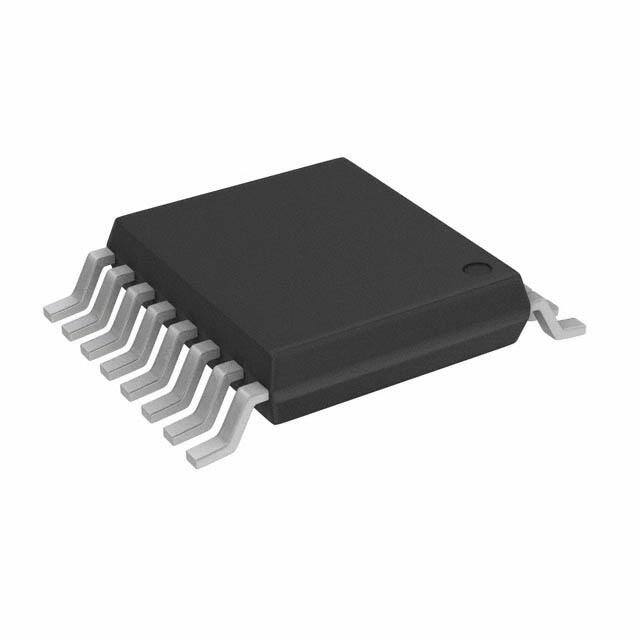
ICGOO电子元器件商城为您提供TDA5101由Infineon设计生产,在icgoo商城现货销售,并且可以通过原厂、代理商等渠道进行代购。 TDA5101价格参考¥询价-¥询价。InfineonTDA5101封装/规格:RF 发射器, RF Transmitter ASK, FSK 315MHz 5dBm 20 kbps PCB, Surface Mount Antenna 16-TSSOP (0.173", 4.40mm Width)。您可以下载TDA5101参考资料、Datasheet数据手册功能说明书,资料中有TDA5101 详细功能的应用电路图电压和使用方法及教程。
TDA5101 是英飞凌科技(Infineon Technologies)推出的一款适用于无线通信领域的 RF 发射器芯片。其主要应用场景包括以下方面:

 1. 汽车电子领域
   - 无钥匙进入系统 (RKE):TDA5101 可用于汽车的遥控钥匙发射模块,实现车辆的远程解锁、锁止和启动功能。
   - 轮胎压力监测系统 (TPMS):作为 RF 发射器,该芯片能够将轮胎压力传感器采集的数据发送到接收端,确保行车安全。
   - 车载通信模块:支持短距离无线通信,例如车与车之间的信息交换或车与基础设施的交互。

 2. 智能家居
   - 无线遥控设备:可用于家庭自动化系统中的遥控发射器,例如窗帘控制、灯光调节等。
   - 安防报警系统:通过 RF 技术将传感器检测到的异常信号(如门窗开关状态、烟雾报警)发送到中央控制器。

 3. 工业应用
   - 无线传感器网络 (WSN):TDA5101 能够在工业环境中用作数据采集节点的 RF 发射器,将温度、湿度、振动等信息传输至监控中心。
   - 资产追踪与管理:在物流和仓储中,该芯片可集成到标签设备中,用于实时位置跟踪和状态更新。

 4. 消费电子
   - 玩具与游戏设备:支持无线互动功能,例如遥控玩具车、无人机或其他智能娱乐产品。
   - 健康与健身设备:可用于心率监测器、步数计等可穿戴设备的数据传输,将信息发送到手机或其他终端。

 5. 医疗设备
   - 便携式医疗仪器:如血糖仪、血压计等,可通过 TDA5101 将测量结果以无线方式发送到医生或患者的移动设备上。

 特性总结
TDA5101 具有低功耗、高可靠性以及良好的抗干扰能力,适合需要稳定 RF 性能的应用场景。其工作频率范围通常覆盖常见的 ISM 频段(如 433 MHz、868 MHz 和 915 MHz),便于在全球范围内使用。此外,它还支持多种调制模式(如 ASK、FSK),可根据具体需求灵活配置。
| 参数 | 数值 |
| 产品目录 | |
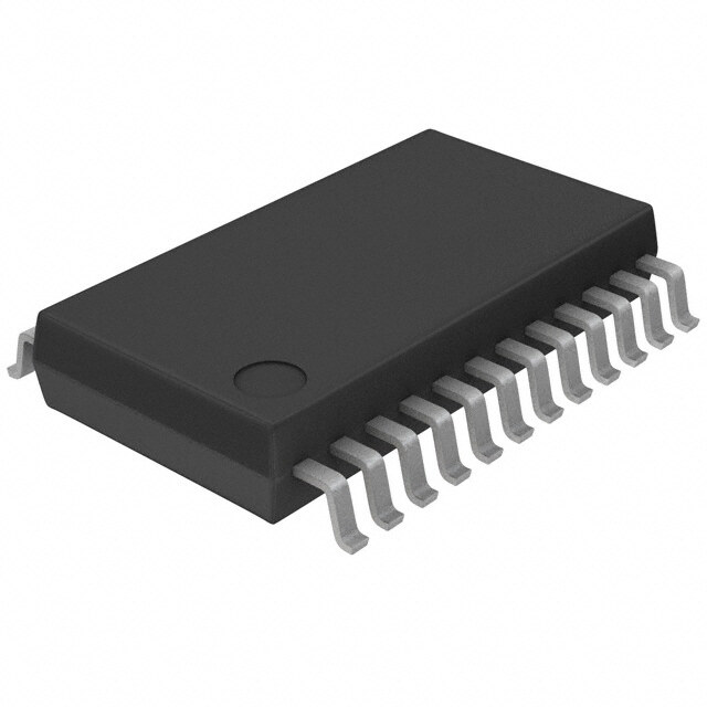
| 描述 | TRANSMITTER ASK/FSK P-TSSOP-16 |
| 产品分类 | |
| 品牌 | Infineon Technologies |
| 数据手册 | |
| 产品图片 |
|
| 产品型号 | TDA5101 |
| rohs | 含铅 / 不符合限制有害物质指令(RoHS)规范要求 |
| 产品系列 | - |
| 其它名称 | TDA5101INCT |
| 功率-输出 | 5dBm |
| 包装 | 剪切带 (CT) |
| 天线连接器 | PCB,表面贴装 |
| 存储容量 | - |
| 封装/外壳 | 16-TSSOP(0.173",4.40mm 宽) |
| 工作温度 | -25°C ~ 85°C |
| 应用 | 警报系统,通信系统 |
| 数据接口 | PCB,表面贴装 |
| 数据速率(最大值) | 20 kbps |
| 标准包装 | 1 |
| 特性 | - |
| 电压-电源 | 2.1 V ~ 4 V |
| 电流-传输 | 7mA |
| 调制或协议 | ASK,FSK |
| 频率 | 315MHz |


- 商务部:美国ITC正式对集成电路等产品启动337调查
- 曝三星4nm工艺存在良率问题 高通将骁龙8 Gen1或转产台积电
- 太阳诱电将投资9.5亿元在常州建新厂生产MLCC 预计2023年完工
- 英特尔发布欧洲新工厂建设计划 深化IDM 2.0 战略
- 台积电先进制程称霸业界 有大客户加持明年业绩稳了
- 达到5530亿美元!SIA预计今年全球半导体销售额将创下新高
- 英特尔拟将自动驾驶子公司Mobileye上市 估值或超500亿美元
- 三星加码芯片和SET,合并消费电子和移动部门,撤换高东真等 CEO
- 三星电子宣布重大人事变动 还合并消费电子和移动部门
- 海关总署:前11个月进口集成电路产品价值2.52万亿元 增长14.8%


PDF Datasheet 数据手册内容提取
Wireless Components ASK/FSK Transmitter 315 MHz TDA 5101 Version 1.6 Specification October 2001
Revision History Current Version: 1.6 as of October 2001 Previous Version: 1.5, March 2001 Page Page Subjects (major changes since last revision) (in previous (in current Version) Version) 2-2, 5-3, 5-6 2-2, 5-3, 5-6 Frequency range increased 3-3 ... 3-6 3-3 ... 3-6 ESD-structures added to interface schematics 3-10, 5-3 3-10, 5-3 Typical value for Power-Down-Mode current added 5-2 5-2 Supply voltage range added to Absolute Maximum Ratings 5-3, 5-6 5-3, 5-6 Loop filter voltages adapted 5-4, 5-7 5-4, 5-7 Saturation voltage of Clock Driver Output reduced 5-5, 5-8 5-5, 5-8 Output Power Tolerances reduced ABM®, AOP®, ARCOFI®, ARCOFI®-BA, ARCOFI®-SP, DigiTape®, EPIC®-1, EPIC®-S, ELIC®, FALC®54, FALC®56, FALC®-E1, FALC®-LH, IDEC®, IOM®, IOM®-1, IOM®-2, IPAT®-2, ISAC®-P, ISAC®-S, ISAC®-S TE, ISAC®-P TE, ITAC®, IWE®, MUSAC®-A, OCTAT®-P, QUAT®-S, SICAT®, SICOFI®, SICOFI®- 2, SICOFI®-4, SICOFI®-4µC, SLICOFI® are registered trademarks of InfineonTechnologiesAG. ACE™, ASM™, ASP™, POTSWIRE™, QuadFALC™, SCOUT™ are trademarks of InfineonTechnologiesAG. Edition 15.02.2001 Published by Infineon Technologies AG, Balanstraße 73, 81541 München © InfineonTechnologiesAG 2001. All Rights Reserved. Attention please! As far as patents or other rights of third parties are concerned, liability is only assumed for components, not for applications, processes and circuits im- plemented within components or assemblies. The information describes the type of component and shall not be considered as assured characteristics. Terms of delivery and rights to change design reserved. Due to technical requirements components may contain dangerous substances. For information on the types in question please contact your nearest InfineonTechnologies Office. InfineonTechnologiesAG is an approved CECC manufacturer. Packing Please use the recycling operators known to you. We can also help you – get in touch with your nearest sales office. By agreement we will take packing material back, if it is sorted. You must bear the costs of transport. For packing material that is returned to us unsorted or which we are not obliged to accept, we shall have to invoice you for any costs incurred. Components used in life-support devices or systems must be expressly authorized for such purpose! Critical components1 of the InfineonTechnologiesAG, may only be used in life-support devices or systems2 with the express written approval of the InfineonTechnologiesAG. 1 A critical component is a component used in a life-support device or system whose failure can reasonably be expected to cause the failure of that life- support device or system, or to affect its safety or effectiveness of that device or system. 2 Life support devices or systems are intended (a) to be implanted in the human body, or (b) to support and/or maintain and sustain human life. If they fail, it is reasonable to assume that the health of the user may be endangered.
1 Table of Contents 1 Table of Contents . . . . . . . . . . . . . . . . . . . . . . . . . . . . . . . . . . . . . . . . . . . . . . . . . . . . . . . . . . . . 1-i 2 Product Description . . . . . . . . . . . . . . . . . . . . . . . . . . . . . . . . . . . . . . . . . . . . . . . . . . . . . . . . . . 2-1 2.1 Overview. . . . . . . . . . . . . . . . . . . . . . . . . . . . . . . . . . . . . . . . . . . . . . . . . . . . . . . . . . . . . . . 2-2 2.2 Applications . . . . . . . . . . . . . . . . . . . . . . . . . . . . . . . . . . . . . . . . . . . . . . . . . . . . . . . . . . . . 2-2 2.3 Features. . . . . . . . . . . . . . . . . . . . . . . . . . . . . . . . . . . . . . . . . . . . . . . . . . . . . . . . . . . . . . . 2-2 2.4 Package Outlines. . . . . . . . . . . . . . . . . . . . . . . . . . . . . . . . . . . . . . . . . . . . . . . . . . . . . . . . 2-3 3 Functional Description . . . . . . . . . . . . . . . . . . . . . . . . . . . . . . . . . . . . . . . . . . . . . . . . . . . . . . . . 3-1 3.1 Pin Configuration . . . . . . . . . . . . . . . . . . . . . . . . . . . . . . . . . . . . . . . . . . . . . . . . . . . . . . . . 3-2 3.2 Pin Definitions and Functions. . . . . . . . . . . . . . . . . . . . . . . . . . . . . . . . . . . . . . . . . . . . . . . 3-3 3.3 Functional Block diagram. . . . . . . . . . . . . . . . . . . . . . . . . . . . . . . . . . . . . . . . . . . . . . . . . . 3-7 3.4 Functional Blocks. . . . . . . . . . . . . . . . . . . . . . . . . . . . . . . . . . . . . . . . . . . . . . . . . . . . . . . . 3-8 4 Applications. . . . . . . . . . . . . . . . . . . . . . . . . . . . . . . . . . . . . . . . . . . . . . . . . . . . . . . . . . . . . . . . . 4-1 4.1 50 Ohm-Output Testboard Schematic . . . . . . . . . . . . . . . . . . . . . . . . . . . . . . . . . . . . . . . . 4-2 4.2 50 Ohm-Output Testboard Layout . . . . . . . . . . . . . . . . . . . . . . . . . . . . . . . . . . . . . . . . . . . 4-3 4.3 Bill of material (50 Ohm-Output Testboard) . . . . . . . . . . . . . . . . . . . . . . . . . . . . . . . . . . . . 4-4 4.4 Hints. . . . . . . . . . . . . . . . . . . . . . . . . . . . . . . . . . . . . . . . . . . . . . . . . . . . . . . . . . . . . . . . . . 4-5 4.5 Application Board Schematic . . . . . . . . . . . . . . . . . . . . . . . . . . . . . . . . . . . . . . . . . . . . . . . 4-8 4.6 Application Board Layout . . . . . . . . . . . . . . . . . . . . . . . . . . . . . . . . . . . . . . . . . . . . . . . . . . 4-9 4.7 Bill of material (Application Board). . . . . . . . . . . . . . . . . . . . . . . . . . . . . . . . . . . . . . . . . . . 4-10 4.8 Application Board Photo. . . . . . . . . . . . . . . . . . . . . . . . . . . . . . . . . . . . . . . . . . . . . . . . . . . 4-11 5 Reference. . . . . . . . . . . . . . . . . . . . . . . . . . . . . . . . . . . . . . . . . . . . . . . . . . . . . . . . . . . . . . . . . . . 5-1 5.1 Absolute Maximum Ratings . . . . . . . . . . . . . . . . . . . . . . . . . . . . . . . . . . . . . . . . . . . . . . . . 5-2 5.2 Operating Range . . . . . . . . . . . . . . . . . . . . . . . . . . . . . . . . . . . . . . . . . . . . . . . . . . . . . . . . 5-2 5.3 AC/DC Characteristics . . . . . . . . . . . . . . . . . . . . . . . . . . . . . . . . . . . . . . . . . . . . . . . . . . . . 5-3
TDA 5101 Product Info Product Info General Description The TDA 5101 is a single chip ASK/ Package FSK transmitter for the frequency band 311-317 MHz. The IC offers a high level of integration and needs only a few external components. The device con- tains a fully integrated PLL synthesizer and a high efficiency power amplifier to drive a loop antenna. A special circuit design and an unique power amplifier design are used to save current con- sumption and therefore to save battery life. Additionally features like a power down mode, a low power detect and a divided clock output are implemented. The IC can be used for both ASK and FSK modulation. Features (cid:1) fully integrated frequency synthe- (cid:1) voltage supply range 2.1 - 4 V sizer (cid:1) power down mode (cid:1) VCO without external components (cid:1) low voltage sensor (cid:1) high efficiency power amplifier (cid:1) programmable divided clock output (cid:1) frequency range 311-317 MHz for µC (cid:1) ASK/FSK modulation (cid:1) low external component count (cid:1) low supply current (typically 7mA) Applications (cid:1) Keyless entry systems (cid:1) Alarm systems (cid:1) Remote control systems (cid:1) Communication systems Ordering Information Type Ordering Code Package TDA 5101 Q67036-A1120 P-TSSOP-16 available on tape and reel Wireless Components Product Info Specification, October 2001
2 Product Description Contents of this Chapter 2.1 Overview. . . . . . . . . . . . . . . . . . . . . . . . . . . . . . . . . . . . . . . . . . . . . . .2-2 2.2 Applications . . . . . . . . . . . . . . . . . . . . . . . . . . . . . . . . . . . . . . . . . . . .2-2 2.3 Features . . . . . . . . . . . . . . . . . . . . . . . . . . . . . . . . . . . . . . . . . . . . . . .2-2 2.4 Package Outlines . . . . . . . . . . . . . . . . . . . . . . . . . . . . . . . . . . . . . . . .2-3
TDA 5101 Product Description 2.1 Overview The TDA 5101 is a single chip ASK/FSK transmitter for the frequency band 311- 317 MHz. The IC offers a high level of integration and needs only a few external components. The device contains a fully integrated PLL synthesizer and a high efficiency power amplifier to drive a loop antenna. A special circuit design and an unique power amplifier design are used to save current consumption and therefore to save battery life. Additional features like a power down mode, a low power detect and a divided clock output are implemented. The IC can be used for both ASK and FSK modulation. 2.2 Applications (cid:1) Keyless entry systems (cid:1) Remote control systems (cid:1) Alarm systems (cid:1) Communication systems 2.3 Features (cid:1) fully integrated frequency synthesizer (cid:1) VCO without external components (cid:1) high efficiency power amplifier (cid:1) frequency range 311-317 MHz (cid:1) ASK/FSK modulation (cid:1) low supply current (typically 7 mA) (cid:1) voltage supply range 2.1 - 4 V (cid:1) power down mode (cid:1) low voltage sensor (cid:1) programmable divided clock output for µC (cid:1) low external component count Wireless Components 2 - 2 Specification, October 2001
TDA 5101 Product Description 2.4 Package Outlines Figure 2-1 P-TSSOP-16 Wireless Components 2 - 3 Specification, October 2001
3 Functional Description Contents of this Chapter 3.1 Pin Configuration. . . . . . . . . . . . . . . . . . . . . . . . . . . . . . . . . . . . . . .3-2 3.2 Pin Definitions and Functions . . . . . . . . . . . . . . . . . . . . . . . . . . . . .3-3 3.3 Functional Block diagram . . . . . . . . . . . . . . . . . . . . . . . . . . . . . . . .3-7 3.4 Functional Blocks. . . . . . . . . . . . . . . . . . . . . . . . . . . . . . . . . . . . . . .3-8 3.4.1 PLL Synthesizer. . . . . . . . . . . . . . . . . . . . . . . . . . . . . . . . . . . . . . . .3-8 3.4.2 Crystal Oscillator . . . . . . . . . . . . . . . . . . . . . . . . . . . . . . . . . . . . . . .3-8 3.4.3 Power Amplifier . . . . . . . . . . . . . . . . . . . . . . . . . . . . . . . . . . . . . . . .3-9 3.4.4 Low Power Detect . . . . . . . . . . . . . . . . . . . . . . . . . . . . . . . . . . . . . .3-9 3.4.5 Power Modes. . . . . . . . . . . . . . . . . . . . . . . . . . . . . . . . . . . . . . . . .3-10 3.4.5.1 Power Down Mode . . . . . . . . . . . . . . . . . . . . . . . . . . . . . . . . . . . .3-10 3.4.5.2 PLL Enable Mode . . . . . . . . . . . . . . . . . . . . . . . . . . . . . . . . . . . . .3-10 3.4.5.3 Transmit Mode. . . . . . . . . . . . . . . . . . . . . . . . . . . . . . . . . . . . . . . .3-10 3.4.5.4 Power mode control. . . . . . . . . . . . . . . . . . . . . . . . . . . . . . . . . . . .3-10 3.4.6 Recommended timing diagrams for ASK- and FSK-Modulation . .3-12
TDA 5101 Functional Description 3.1 Pin Configuration PDWN 1 16 CSEL LPD 2 15 FSEL VS 3 14 PAOUT LF 4 13 PAGND TDA 5101 GND 5 12 FSKGND ASKDTA 6 11 FSKOUT FSKDTA 7 10 COSC CLKOUT 8 9 CLKDIV Pin_config.wmf Figure 3-1 IC Pin Configuration Table 3-1 Pin No. Symbol Function 1 PDWN Power Down Mode Control 2 LPD Low Power Detect Output 3 VS Voltage Supply 4 LF Loop Filter 5 GND Ground 6 ASKDTA Amplitude Shift Keying Data Input 7 FSKDTA Frequency Shift Keying Data Input 8 CLKOUT Clock Driver Output 9 CLKDIV Clock Divider Control 10 COSC Crystal Oscillator Input 11 FSKOUT Frequency Shift Keying Switch Output 12 FSKGND Frequency Shift Keying Ground 13 PAGND Power Amplifier Ground 14 PAOUT Power Amplifier Output 15 FSEL Frequency Range Selection: Has to be shorted to ground for 315 MHz operation 16 CSEL Crystal Frequency Selection: Has to be left open Wireless Components 3 - 2 Specification, October 2001
TDA 5101 Functional Description 3.2 Pin Definitions and Functions Table 3-2 Pin Symbol Interface Schematic Function No. 1 PDWN Disable pin for the complete transmitter cir- cuit. V S A logic low (PDWN < 0.7 V) turns off all 40 µA ∗ (ASKDTA+FSKDTA) transmitter functions. 5 kΩ A logic high (PDWN > 1.5 V) gives access to 1 all transmitter functions. "ON" PDWN input will be pulled up by 40 µA inter- 150 kΩ nally by setting FSKDTA or ASKDTA to a logic high-state. 250 kΩ 2 LPD This pin provides an output indicating the low-voltage state of the supply voltage VS. V S VS < 2.15 V will set LPD to the low-state. 40 µA An internal pull-up current of 40 µA gives the 2 output a high-state at supply voltages above 2.15 V. 300 Ω 3 VS This pin is the positive supply of the trans- mitter electronics. An RF bypass capacitor should be con- nected directly to this pin and returned to GND (pin 5) as short as possible. Wireless Components 3 - 3 Specification, October 2001
TDA 5101 Functional Description 4 LF Output of the charge pump and input of the VCO control voltage. V S The loop bandwidth of the PLL is 150 kHz when only the internal loop filter is used. The loop bandwidth may be reduced by 140 pF applying an external RC network referencing 15 pF to the positive supply VS (pin 3). 35 kΩ 10 kΩ V S 4 5 GND General ground connection. 6 ASKDTA Digital amplitude modulation can be V +1.2 V imparted to the Power Amplifier through this S pin. 60 kΩ A logic high (ASKDTA > 1.5 V or open) 6 enables the Power Amplifier. +1.1 V 90 kΩ A logic low (ASKDTA < 0.5 V) disables the Power Amplifier. 50 pF 30 µA 7 FSKDTA Digital frequency modulation can be V +1.2 V imparted to the Xtal Oscillator by this pin. S The VCO-frequency varies in accordance to the frequency of the reference oscillator. 60 kΩ 7 A logic high (FSKDTA > 1.5V or open) +1.1 V sets the FSK switch to a high impedance 90 kΩ state. 30 µA A logic low (FSKDTA < 0.5 V) closes the FSK switch from FSKOUT (pin 11) to FSKGND (pin 12). A capacitor can be switched to the reference crystal network this way. The Xtal Oscillator frequency will be shifted giving the designed FSK frequency deviation. Wireless Components 3 - 4 Specification, October 2001
TDA 5101 Functional Description 8 CLKOUT Clock output to supply an external device. An external pull-up resistor has to be added V S in accordance to the driving requirements of 8 the external device. A clock frequency of 2.46 MHz is selected 300 Ω by a logic low at CLKDIV input (pin9). A clock frequency of 615 kHz is selected by a logic high at CLKDIV input (pin9). 9 CLKDIV This pin is used to select the desired clock division rate for the CLKOUT signal. V +1.2 V V S S A logic low (CLKDIV < 0.2 V) applied to this pin selects the 2.46 MHz output signal at 5 µA CLKOUT (pin 8). 60 kΩ A logic high (CLKDIV open) applied to this 9 pin selects the 615 kHz output signal at +0.8 V 60 kΩ CLKOUT (pin 8). 10 COSC This pin is connected to the reference oscil- lator circuit. V V S S The reference oscillator is working as a neg- ative impedance converter. It presents a 6 kΩ negative resistance in series to an induc- tance at the COSC pin. 10 100 µA 11 FSKOUT This pin is connected to a switch to FSKGND (pin 12). V V S S The switch is closed when the signal at FSKDTA (pin 7) is in a logic low state. 200 µA The switch is open when the signal at FSKDTA (pin 7) is in a logic high state. 1.5 kΩ 11 FSKOUT can switch an additional capacitor to the reference crystal network to pull the crystal frequency by an amount resulting in the desired FSK frequency shift of the trans- 12 mitter output frequency. 12 FSKGND Ground connection for FSK modulation out- put FSKOUT. Wireless Components 3 - 5 Specification, October 2001
TDA 5101 Functional Description 13 PAGND Ground connection of the power amplifier. The RF ground return path of the power amplifier output PAOUT (pin 14) has to be concentrated to this pin. 14 PAOUT RF output pin of the transmitter. 14 A DC path to the positive supply VS has to be supplied by the antenna matching net- work. 13 15 FSEL This pin has to be shorted to ground to select the 315 MHz transmitter frequency VS +1.2 V range. A logic low (FSEL < 0.5 V) applied to this pin 30 kΩ sets the transmitter to the 315 MHz fre- 15 quency range. +1.1 V 90 kΩ A logic high (FSEL open) applied to this pin 30 µA sets the transmitter to the 630 MHz fre- quency range. 16 CSEL This pin is used to select the desired refer- ence frequency. V +1.2 V V S S A logic high (CSEL open) applied to this pin 5 µA 60 kΩ sets the internal frequency divider to accept 16 a reference frequency of 9.84 MHz. +0.8 V 60 kΩ Wireless Components 3 - 6 Specification, October 2001
TDA 5101 Functional Description 3.3 Functional Block diagram PowerAmplifierOutput PowerAmplifierGround 4 3 1 1 On werMP 5 und PoA Gro eV Low PowerDetect Output 2 Low VoltagSensor 2.2 :1/2 15 equency Selectw for 315 MHz Positive SupplyVS 3 PowerSupply VCO LF 4 LoopFrFilterlo PowerDownControl 61 OR 128/64 16 CrystalSelectways open SKataput : al ADn I D 7 F SKataput P FDIn :2/8:4/16 8 ClockOutput L Asc TO X 2 1 0 9 1 1 1 z FSKGround FSKSwitch Crystal84 MHz Clock OutputFrequencySelect615/2.46 MH 9, 0. Funct_Block_Diagram.wmf Figure 3-2 Functional Block diagram Wireless Components 3 - 7 Specification, October 2001
TDA 5101 Functional Description 3.4 Functional Blocks 3.4.1 PLL Synthesizer The Phase Locked Loop synthesizer consists of a Voltage Controlled Oscillator (VCO), an asynchronous divider chain, a phase detector, a charge pump and a loop filter. It is fully implemented on chip. The tuning circuit of the VCO consist- ing of spiral inductors and varactor diodes is on chip, too. Therefore no addi- tional external components are necessary. The nominal center frequency of the VCO is 630 MHz. The oscillator signal is fed both, to the synthesizer divider chain and to the power amplifier. The overall division ratio of the asynchronous divider chain is 64. The phase detector is a Type IV PD with charge pump. The passive loop filter is realized on chip. In all 315 MHz applications, the FSEL pin is shorted to ground (logic low) and the CSEL pin is not connected (logic high). 3.4.2 Crystal Oscillator The crystal oscillator operates at 9.84 MHz. Frequencies of 615 kHz or 2.46 MHz are available at the clock output CLKOUT (pin 8) to drive the clock input of a micro controller. The frequency at CLKOUT (pin 8) is controlled by the signal at CLKDIV (pin 9) Table 3-3 CLKDIV (pin 9) CLKOUT Frequency Low1) 2.46 MHz Open2) 615 kHz 1) Low: Voltage at pin < 0.2 V 2) Open: Pin open To achieve FSK transmission, the oscillator frequency can be detuned by a fixed amount by switching an external capacitor via FSKOUT (pin 11). The condition of the switch is controlled by the signal at FSKDTA (pin 7). Table 3-4 FSKDTA (pin7) FSK Switch Low1) CLOSED Open2), High3) OPEN 1) Low: Voltage at pin < 0.5 V 2) Open: Pin open 3) High: Voltage at pin > 1.5 V Wireless Components 3 - 8 Specification, October 2001
TDA 5101 Functional Description 3.4.3 Power Amplifier For operation at 315 MHz, the power amplifier is fed with the VCO frequency divided by 2. It is possible to feed the power amplifier directly from the voltage controlled oscillator. This is controlled by FSEL (pin 15) as described in the table below. Table 3-5 FSEL (pin 15) Radiated Frequency Band Low1) 315 MHz Open2) 630 MHz 1) Low: Voltage at pin < 0.5 V 2) Open: Pin open In all 315 MHz applications, the pin FSEL is connected to ground. The Power Amplifier can be switched on and off by the signal at ASKDTA (pin 6). Table 3-6 ASKDTA (pin 6) Power Amplifier Low1) OFF Open2), High3) ON 1) Low: Voltage at pin < 0.5 V 2) Open: Pin open 3) High: Voltage at pin > 1.5 V The Power Amplifier has an Open Collector output at PAOUT (pin 14) and requires an external pull-up coil to provide bias. The coil is part of the tuning and matching LC circuitry to get best performance with the external loop antenna. To achieve the best power amplifier efficiency, the high frequency voltage swing at PAOUT (pin 14) should be twice the supply voltage. The power amplifier has its own ground pin PAGND (pin 13) in order to reduce the amount of coupling to the other circuits. 3.4.4 Low Power Detect The supply voltage is sensed by a low power detector. When the supply voltage drops below 2.15 V, the output LPD (pin 2) switches to the low-state. To mini- mize the external component count, an internal pull-up current of 40 µA gives the output a high-state at supply voltages above 2.15 V. The output LPD (pin 2) can either be connected to ASKDTA (pin 6) to switch off the PA as soon as the supply voltage drops below 2.15 V or it can be used to inform a micro-controller to stop the transmission after the current data packet. Wireless Components 3 - 9 Specification, October 2001
TDA 5101 Functional Description 3.4.5 Power Modes The IC provides three power modes, the POWER DOWN MODE, the PLL ENABLE MODE and the TRANSMIT MODE. 3.4.5.1 Power Down Mode In the POWER DOWN MODE the complete chip is switched off. The current consumption is typically 0.3 nA at 3 V 25°C. 3.4.5.2 PLL Enable Mode In the PLL ENABLE MODE the PLL is switched on but the power amplifier is turned off to avoid undesired power radiation during the time the PLL needs to settle. The turn on time of the PLL is determined mainly by the turn on time of the crystal oscillator and is less than 1 msec when the specified crystal is used. The current consumption is typically 3.5 mA. 3.4.5.3 Transmit Mode In the TRANSMIT MODE the PLL is switched on and the power amplifier is turned on too. The current consumption of the IC is typically 7 mA when using a proper trans- forming network at PAOUT, see Figure 4-1. 3.4.5.4 Power mode control The bias circuitry is powered up via a voltage V > 1.5 V at the pin PDWN (pin 1). When the bias circuitry is powered up, the pins ASKDTA and FSKDTA are pulled up internally. Forcing the voltage at the pins low overrides the internally set state. Alternatively, if the voltage at ASKDTA or FSKDTA is forced high externally, the PDWN pin is pulled up internally via a current source. In this case, it is not nec- essary to connect the PDWN pin, it is recommended to leave it open. The principle schematic of the power mode control circuitry is shown in Figure 3-5. Wireless Components 3 - 10 Specification, October 2001
TDA 5101 Functional Description PDWN ASKDTA OR FSKDTA On Bias Source 120 kΩ e g a Volt 120 kΩ FSKOUT s FSK a On Bi 315 PLL PA PAOUT MHz IC Power_Mode.wmf Figure 3-5 Power mode control circuitry Table 3-7 provides a listing of how to get into the different power modes Table 3-7 PDWN FSKDTA ASKDTA MODE Low1) Low, Open Low, Open POWER DOWN Open2) Low Low High3) Low, Open, High Low PLL ENABLE Open High Low High Low, Open, High Open, High Open High Open, High TRANSMIT Open Low, Open, High High 1) Low: Voltage at pin < 0.7 V (PDWN) Voltage at pin < 0.5 V (FSKDTA, ASKDTA) 2) Open: Pin open 3) High: Voltage at pin > 1.5 V Other combinations of the control pins PDWN, FSKDTA and ASKDTA are not recommended. Wireless Components 3 - 11 Specification, October 2001
TDA 5101 Functional Description 3.4.6 Recommended timing diagrams for ASK- and FSK-Modulation ASK Modulation using FSKDTA and ASKDTA, PDWN not connected Modes: Power Down PLL Enable Transmit High FSKDTA Low to t DATA Open, High ASKDTA Low to t min. 1 msec. ASK_mod.wmf Figure 3-6 ASK Modulation FSK Modulation using FSKDTA and ASKDTA, PDWN not connected Modes: Power Down PLL Enable Transmit DATA High FSKDTA Low to t High ASKDTA Low to t min. 1 msec. FSK_mod.wmf Figure 3-7 FSK Modulation Wireless Components 3 - 12 Specification, October 2001
TDA 5101 Functional Description Alternative ASK Modulation, FSKDTA not connected. Modes: Power Down PLL Enable Transmit High PDWN Low to t DATA Open, High ASKDTA Low to t min. 1 msec. Alt_ASK_mod.wmf Figure 3-8 Alternative ASK Modulation Alternative FSK Modulation Modes: Power Down PLL Enable Transmit High PDWN Low to t Open, High ASKDTA Low to t DATA Open, High FSKDTA Low to t min. 1 msec. Alt_FSK_mod.wmf Figure 3-9 Alternative FSK Modulation Wireless Components 3 - 13 Specification, October 2001
4 Applications Contents of this Chapter 4.1 50 Ohm-Output Testboard Schematic . . . . . . . . . . . . . . . . . . . . . . . .4-2 4.2 50 Ohm-Output Testboard Layout . . . . . . . . . . . . . . . . . . . . . . . . . . .4-3 4.3 Bill of material (50 Ohm-Output Testboard) . . . . . . . . . . . . . . . . . . . .4-4 4.4 Hints . . . . . . . . . . . . . . . . . . . . . . . . . . . . . . . . . . . . . . . . . . . . . . . . . .4-5 4.5 Application Board Schematic . . . . . . . . . . . . . . . . . . . . . . . . . . . . . . .4-8 4.6 Application Board Layout . . . . . . . . . . . . . . . . . . . . . . . . . . . . . . . . . .4-9 4.7 Bill of material (Application Board) . . . . . . . . . . . . . . . . . . . . . . . . . .4-10 4.8 Application Board Photo. . . . . . . . . . . . . . . . . . . . . . . . . . . . . . . . . .4-11
TDA 5101 Applications 4.1 50 Ohm-Output Testboard Schematic X2SMA C8 C2 C4 L2 L1 VCC C7 C3 C6 Q1 0.615 (2.46) 6 5 4 3 2 1 0 9 MHz 1 1 1 1 1 1 1 TDA5101 1 2 3 4 5 6 7 8 C1 C C V T1 R3A VCC R3F R4 R2 ASK FSK C5 R1 X1SMA 50ohm_test_v5.wmf Figure 4-1 50 Ω-Output testboard schematic Wireless Components 4 - 2 Specification, October 2001
TDA 5101 Applications 4.2 50 Ohm-Output Testboard Layout Figure 4-2 Top Side of TDA 5101-Testboard with 50 Ω-Output. It is the same testboard as for the TDA 5100. Figure 4-3 Bottom Side of TDA 5101-Testboard with 50 Ω-Output. It is the same testboard as for the TDA 5100. Wireless Components 4 - 3 Specification, October 2001
TDA 5101 Applications 4.3 Bill of material (50 Ohm-Output Testboard) Table 4-1 Bill of material Part ASK 315 MHz FSK 315 MHz Specification R1 4.7 kΩ 4.7 kΩ 0805, ± 5% R2 12 kΩ 0805, ± 5% R3A 15 kΩ 0805, ± 5% R3F 15 kΩ 0805, ± 5% R4 open open 0805, ± 5% C1 47 nF 47 nF 0805, X7R, ± 10% C2 56 pF 56 pF 0805, COG, ± 5% C3 5.6 pF 5.6 pF 0805, COG, ± 0.1 pF C4 330 pF 330 pF 0805, COG, ± 5% C5 1 nF 1 nF 0805, X7R, ± 10% C6 8.2 pF 8.2 pF 0805, COG, ± 0.1 pF C7 0 Ω Jumper 47 pF 0805, COG, ± 5% 0805, 0Ω Jumper C8 22 pF 22 pF 0805, COG, ± 5% L1 220 nH 220 nH TOKO LL2012-J L2 56 nH 56 nH TOKO LL2012-J Q3 9.843745 MHz, 9.843745 MHz, Tokyo Denpa TSS-3B CL=12pF CL=12pF 9843.75 kHz Spec.No. 20-18905 IC1 TDA 5101 TDA 5101 T1 Push-button Push-button replaced by a short B1 Battery clip Battery clip HU2031-1, RENATA X1 SMA-S SMA-S SMA standing X2 SMA-S SMA-S SMA standing Wireless Components 4 - 4 Specification, October 2001
TDA 5101 Applications 4.4 Hints 1. Application Hints on the crystal oscillator As mentioned before, the crystal oscillator achieves a turn on time less than 1 msec. To achieve this, a NIC oscillator type is implemented in the TDA 5101. The input impedance of this oscillator is a negative resistance in series to an inductance. Therefore the load capacitance of the crystal CL (specified by the crystal supplier) is transformed to the capacitance Cv. -R L f, CL Cv IC 1 Cv= Formula 1) 1 +ω2L CL CL: crystal load capacitance for nominal frequency ω: angular frequency L: inductivity of the crystal oscillator Example for the ASK-Mode: Referring to the application circuit, in ASK-Mode the capacitance C7 is replaced by a short to ground. Assume a crystal frequency of 9.84 MHz and a crystal load capacitance of CL = 12 pF. The inductance L is specified within the electrical characteristics at 9.84 MHz to a value of 11 µH. Therefore C6 is calculated to 8.0 pF. 1 Cv= =C6 1 +ω2L CL Wireless Components 4 - 5 Specification, October 2001
TDA 5101 Applications Example for the FSK-Mode: FSK modulation is achieved by switching the load capacitance of the crystal as shown below. FSKDTA FSKOUT Csw -R L f, CL Cv1 Cv2 COSC IC The frequency deviation of the crystal oscillator is multiplied with the divider factor N of the Phase Locked Loop to the output of the power amplifier. In case of small frequency deviations (up to +/- 1000 ppm), the two desired load capacitances can be calculated with the formula below. ∆f 2(C0+CL) CL(cid:1)C0 (1+ ) N* f1 C1 CL± = ∆f 2(C0+CL) 1± (1+ ) N* f1 C1 C : crystal load capacitance for nominal frequency L C : shunt capacitance of the crystal 0 f: frequency ω: ω = 2πf: angular frequency N: division ratio of the PLL df: peak frequency deviation Because of the inductive part of the TDA 5101, these values must be corrected by formula 1). The value of Cv± can be calculated. Wireless Components 4 - 6 Specification, October 2001
TDA 5101 Applications If the FSK switch is closed, Cv- is equal to Cv1 (C6 in the application diagram). If the FSK switch is open, Cv2 (C7 in the application diagram) can be calculated. Csw∗Cv1−(Cv+)∗(Cv1+Csw) Cv2=C7= (Cv+)−Cv1 Csw: parallel capacitance of the FSK switch (3 pF) Remark: These calculations are only approximations. The necessary values depend on the layout also and must be adapted for the specific application board. 2. Design hints on the buffered clock output (CLKOUT) The CLKOUT pin is an open collector output. An external pull up resistor (RL) should be connected between this pin and the positive supply voltage. The value of RL is depending on the clock frequency and the load capacitance CLD (PCB board plus input capacitance of the microcontroller). RL can be calculated to: 1 RL= fCLKOUT*8*CLD Table 4-2 fCLKOUT= fCLKOUT= 615 kHz 2.46 MHz [ ] [ ] [ ] [ ] CLD pF RL kOhm CLD pF RL kOhm 5 39 5 10 10 18 10 4.7 20 10 20 2.2 Remark: To achieve a low current consumption and a low spurious radiation, the largest possible RL should be chosen. Wireless Components 4 - 7 Specification, October 2001
TDA 5101 Applications 4.5 Application Board Schematic VCC R4 C3 Antenna C2 L1 C7 C4 C6 Q3 0.615 (2.46) 6 5 4 3 2 1 0 9 MHz 1 1 1 1 1 1 1 TDA5101 1 2 3 4 5 6 7 8 C1 C C V T1 R2A VCC R2F R3A R3F ASK FSK C5 R1 VCC 8 7 6 5 HCS360 1 2 3 4 Application_circuit.wmf Figure 4-4 Application board schematic Wireless Components 4 - 8 Specification, October 2001
TDA 5101 Applications 4.6 Application Board Layout Figure 4-5 Top Side of TDA 5101-Application Board Figure 4-6 Bottom Side of TDA 5101-Application Board Wireless Components 4 - 9 Specification, October 2001
TDA 5101 Applications 4.7 Bill of material (Application Board) Table 4-3 Bill of material Part 315 MHz ASK 315 MHz FSK Specification R1 4.7 kΩ 4.7 kΩ 0805, ± 5% R2A 15 kΩ 0805, ± 5% R2F 12 kΩ 0805, ± 5% R3A 15 kΩ 15 kΩ 0805, ± 5% R3F 12 kΩ 0805, ± 5% R4 1 kΩ 1 kΩ 0805, ± 5% C1 47 nF 47 nF 0805, X7R, ± 10% C2 18 pF 18 pF 0805, COG, ± 1% C3 330 pF 330 pF 0805, COG, ± 10% C4 10 pF 10 pF 0805, COG, ± 1% C5 4.7 nF 4.7 nF 0805, X7R, ± 10% C6 8.2 pF 8.2 pF 0805, COG, ± 0.1 pF C7 0 Ω 47 pF 0805, COG, ± 10% 0805, 0Ω Jumper L1 39 nH 39 nH TOKO LL2012-J Q3 9.84375 MHz 9.84375 MHz Tokyo Denpa TSS-3B 9843.75 CL=12pF CL=12pF kHz Spec.No. 20-18905 IC1 TDA 5101 TDA 5101 IC2 HCS360 HCS360 Microchip B1 Battery clip Battery clip HU2031-1, RENATA T1 Push-button Push-button STTSKHMPW, ALPS Wireless Components 4 - 10 Specification, October 2001
TDA 5101 Applications 4.8 Application Board Photo TDA5101ApplBoard.jpg Figure 4-7 Photo of Application Board TDA 5101 Wireless Components 4 - 11 Specification, October 2001
5 Reference Contents of this Chapter 5.1 Absolute Maximum Ratings . . . . . . . . . . . . . . . . . . . . . . . . . . . . . . . .5-2 5.2 Operating Range . . . . . . . . . . . . . . . . . . . . . . . . . . . . . . . . . . . . . . . .5-2 5.3 AC/DC Characteristics . . . . . . . . . . . . . . . . . . . . . . . . . . . . . . . . . . . .5-3 5.3.1 AC/DC Characteristics at 3V, 25°C . . . . . . . . . . . . . . . . . . . . . . . . . .5-3 5.3.2 AC/DC Characteristics at 2.1 V ... 4.0 V, -25°C ... +85°C. . . . . . . . . .5-6
TDA 5101 Reference 5.1 Absolute Maximum Ratings The AC / DC characteristic limits are not guaranteed. The maximum ratings must not be exceeded under any circumstances, not even momentarily and individually, as permanent damage to the IC may result. Table 5-1 Parameter Symbol Limit Values Unit Remarks Min Max Junction Temperature T -40 150 °C J Storage Temperature T -40 125 °C s Thermal Resistance R 230 K/W thJA Supply voltage V -0.3 4.0 V S ESD integrity, all pins V -1 +1 kV 100 pF, 1500 Ω ESD Ambient Temperature under bias: T =-25 to +85°C A 5.2 Operating Range Within the operational range the IC operates as described in the circuit description. Table 5-2 Parameter Symbol Limit Values Unit Test Conditions Min Max Supply voltage V 2.1 4.0 V S Ambient temperature T -25 85 °C A Wireless Components 5 - 2 Specification, October 2001
TDA 5101 Reference 5.3 AC/DC Characteristics 5.3.1 AC/DC Characteristics at 3V, 25°C Table 5-3 Supply Voltage V = 3 V, Ambient temperature T = 25°C S amb Parameter Symbol Limit Values Unit Test Conditions Min Typ Max Current consumption Power down mode I 0.3 100 nA V (Pins 1, 6 and 7) S PDWN < 0.2 V PLL enable mode I 3.3 4.2 mA S PLL_EN Transmit mode I 7 9 mA Load tank see S TRANSM Figure 4-1 and 4-2 Power Down Mode Control (Pin 1) Power down mode V 0 0.7 V V < 0.2 V PDWN ASKDTA V < 0.2 V FSKDTA PLL enable mode V 1.5 V V V < 0.5 V PDWN S ASKDTA Transmit mode V 1.5 V V V > 1.5 V PDWN S ASKDTA Input bias current PDWN I 30 µA V = V PDWN PDWN S Low Power Detect Output (Pin 2) Internal pull up current I 30 µA V = 2.3 V ... V LPD1 S S Input current low voltage I 1 mA V = 1.9 V ... 2.1 V LPD2 S Loop Filter (Pin 4) VCO tuning voltage V V - 1.5 V - 0.7 V f = 630 MHz LF S S VCO Output frequency range f 305 315 324 MHz V -V = 0.4V...1.9V OUT, 315 S LF 315 MHz-band V = 0 V FSEL ASK Modulation Data Input (Pin 6) ASK Transmit disabled V 0 0.5 V ASKDTA ASK Transmit enabled V 1.5 V V ASKDTA S Input bias current ASKDTA I 30 µA V = V ASKDTA ASKDTA S Input bias current ASKDTA I -20 µA V = 0 V ASKDTA ASKDTA ASK data rate f 20 kHz ASKDTA Wireless Components 5 - 3 Specification, October 2001
TDA 5101 Reference Table 5-3 Supply Voltage V = 3 V, Ambient temperature T = 25°C S amb Parameter Symbol Limit Values Unit Test Conditions Min Typ Max FSK Modulation Data Input (Pin 7) FSK Switch on V 0 0.5 V FSKDTA FSK Switch off V 1.5 V V FSKDTA S Input bias current FSKDTA I 30 µA V = V FSKDTA FSKDTA S Input bias current FSKDTA I -20 µA V = 0 V FSKDTA FSKDTA FSK data rate f 20 kHz FSKDTA Clock Driver Output (Pin 8) Output current (Low) I 1 mA V = V CLKOUT CLKOUT S Output current (High) I 5 µA V = V CLKOUT CLKOUT S Saturation Voltage (Low) V 0.56 V I = 1 mA SATL CLKOUT Clock Divider Control (Pin 9) Setting Clock Driver output V 0 0.2 V CLKDIV frequency f =2.46 MHz CLKOUT Setting Clock Driver output V V pin open CLKDIV frequency f =615 kHz CLKOUT Input bias current CLKDIV I 30 µA V = V CLKDIV CLKDIV S Input bias current CLKDIV I -20 µA V = 0 V CLKDIV CLKDIV Crystal Oscillator Input (Pin 10) Load capacitance C 5 pF COSCmax Serial Resistance of the crys- 100 Ω f = 9.84 MHz tal Input inductance of the 11 µH f = 9.84 MHz COSC pin FSK Switch Output (Pin 11) On resistance R 220 Ω V = 0 V FSKOUT FSKDTA On capacitance C 6 pF V = 0 V FSKOUT FSKDTA Off resistance R 10 kΩ V = V FSKOUT FSKDTA S Off capacitance C 1.5 pF V = V FSKOUT FSKDTA S Wireless Components 5 - 4 Specification, October 2001
TDA 5101 Reference Table 5-3 Supply Voltage V = 3 V, Ambient temperature T = 25°C S amb Parameter Symbol Limit Values Unit Test Conditions Min Typ Max Power Amplifier Output (Pin 14) Output Power1) POUT315 3.5 5 6.5 dBm fOUT = 315 MHz transformed to 50 Ohm VFSEL = 0 V Frequency Range Selection (Pin 15) Transmit frequency 315 MHz V 0 0.5 V FSEL Input bias current FSEL I 30 µA V = V FSEL FSEL S Input bias current FSEL I -20 µA V = 0 V FSEL FSEL Crystal Frequency Selection (Pin 16) Crystal frequency 9.84 MHz V V pin open CSEL Input bias current CSEL I 50 µA V = V CSEL CSEL S Input bias current CSEL I -25 µA V = 0 V CSEL CSEL 1) Power amplifier in overcritical C-operation. Matching circuitry as used in the 50 Ohm-Output Testboard. Tolerances of the passive elements not taken into account. Wireless Components 5 - 5 Specification, October 2001
TDA 5101 Reference 5.3.2 AC/DC Characteristics at 2.1 V ... 4.0 V, -25°C ... +85°C Table 5-4 Supply Voltage V = 2.1 V ... 4.0 V, Ambient temperature T = -25°C ... +85°C S amb Parameter Symbol Limit Values Unit Test Conditions Min Typ Max Current consumption Power down mode I 250 nA V (Pins 1, 6, and 7) S PDWN = 0.2 V PLL enable mode I 3.3 4.6 mA S PLL_EN Transmit mode I 7 9.5 mA Load tank see S TRANSM Figure 4-1 and 4-2 Power Down Mode Control (Pin 1) Power down mode V 0 0.5 V V < 0.2 V PDWN ASKDTA V < 0.2 V FSKDTA PLL enable mode V 1.5 V V V < 0.5 V PDWN S ASKDTA Transmit mode V 1.5 V V V > 1.5 V PDWN S ASKDTA Input bias current PDWN I 30 µA V = V PDWN PDWN S Low Power Detect Output (Pin 2) Internal pull up current I 30 µA V = 2.3 V ... V LPD1 S S Input current low voltage I 1 mA V = 1.9 V ... 2.1 V LPD2 S Loop Filter (Pin 4) VCO tuning voltage V V - 1.8 V - 0.5 V f = 630 MHz LF S S VCO Output frequency range f 311 315 317 MHz V -V = 0.4V...1.9V OUT, 315 S LF 315 MHz-band V = 0 V FSEL ASK Modulation Data Input (Pin 6) ASK Transmit disabled V 0 0.5 V ASKDTA ASK Transmit enabled V 1.5 V V ASKDTA S Input bias current ASKDTA I 30 µA V = V ASKDTA ASKDTA S Input bias current ASKDTA I -20 µA V = 0 V ASKDTA ASKDTA ASK data rate f 20 kHz ASKDTA Wireless Components 5 - 6 Specification, October 2001
TDA 5101 Reference Table 5-4 Supply Voltage V = 2.1 V ... 4.0 V, Ambient temperature T = -25°C ... +85°C S amb Parameter Symbol Limit Values Unit Test Conditions Min Typ Max FSK Modulation Data Input (Pin 7) FSK Switch on V 0 0.5 V FSKDTA FSK Switch off V 1.5 V V FSKDTA S Input bias current FSKDTA I 30 µA V = V FSKDTA FSKDTA S Input bias current FSKDTA I -20 µA V = 0 V FSKDTA FSKDTA FSK data rate f 20 kHz FSKDTA Clock Driver Output (Pin 8) Output current (Low) I 1 mA V = V CLKOUT CLKOUT S Output current (High) I 5 µA V = V CLKOUT CLKOUT S Saturation Voltage (Low)1) VSATL 0.5 V ICLKOUT = 0.8 mA Clock Divider Control (Pin 9) Setting Clock Driver output V 0 0.2 V CLKDIV frequency f =2.46 MHz CLKOUT Setting Clock Driver output V V pin open CLKDIV frequency f =615 kHz CLKOUT Input bias current CLKDIV I 30 µA V = V CLKDIV CLKDIV S Input bias current CLKDIV I -20 µA V = 0 V CLKDIV CLKDIV Crystal Oscillator Input (Pin 10) Load capacitance C 5 pF COSCmax Serial Resistance of the crys- 100 Ω f = 9.84 MHz tal Input inductance of the 11 µH f = 9.84 MHz COSC pin FSK Switch Output (Pin 11) On resistance R 220 Ω V = 0 V FSKOUT FSKDTA On capacitance C 6 pF V = 0 V FSKOUT FSKDTA Off resistance R 10 kΩ V = V FSKOUT FSKDTA S Off capacitance C 1.5 pF V = V FSKOUT FSKDTA S 1) Derating linearly to a saturation voltage of max. 140 mV at I = 0 mA CLKOUT Wireless Components 5 - 7 Specification, October 2001
TDA 5101 Reference Table 5-4 Supply Voltage V = 2.1 V ... 4.0 V, Ambient temperature T = -25°C ... +85°C S amb Parameter Symbol Limit Values Unit Test Conditions Min Typ Max Power Amplifier Output (Pin 14) Output Power 1) at 315 MHz POUT, 315 0.4 2.2 3.5 dBm VS = 2.1 V transformed to 50 Ohm. P 2.5 5 6.9 dBm V = 3.0 V OUT, 315 S VFSEL = 0 V POUT, 315 3.3 6.8 9.4 dBm VS = 4.0 V Frequency Range Selection (Pin 15) Transmit frequency 315 MHz V 0 0.5 V FSEL Input bias current FSEL I 30 µA V = V FSEL FSEL S Input bias current FSEL I -20 µA V = 0 V FSEL FSEL Crystal Frequency Selection (Pin 16) Crystal frequency 9.84 MHz V V pin open CSEL Input bias current CSEL I 50 µA V = V CSEL CSEL S Input bias current CSEL I -25 µA V = 0 V CSEL CSEL 1) Matching circuitry as used in the 50 Ohm-Output Testboard. Range @ 2.1 V, +25°C: 2.2 dBm +/- 1.0 dBm Temperature dependency at 2.1 V: +0.3 dBm@-25°C and -0.8 dBm@+85°C, reference +25°C. Range @ 3.0 V, +25°C: 5.0 dBm +/- 1.5 dBm Temperature dependency at 3.0 V: +0.4 dBm@-25°C and -1.0 dBm@+85°C, reference +25°C. Range @ 4.0 V, +25°C: 6.8 dBm +/- 2.0 dBm Temperature dependency at 4.0 V: +0.6 dBm@-25°C and -1.5 dBm@+85°C, reference +25°C. Tolerances of the passive elements not taken into account. A smaller load impedance reduces the supply-voltage dependency. A higher load impedance reduces the temperature dependency. Wireless Components 5 - 8 Specification, October 2001