ICGOO在线商城 > 射频/IF 和 RFID > RF 放大器 > ADL5605ACPZ-R7
 Datasheet下载
- 型号: ADL5605ACPZ-R7
- 制造商: Analog
- 库位|库存: xxxx|xxxx
- 要求:
| 数量阶梯 | 香港交货 | 国内含税 |
| +xxxx | $xxxx | ¥xxxx |
查看当月历史价格
查看今年历史价格
ADL5605ACPZ-R7产品简介:
ICGOO电子元器件商城为您提供ADL5605ACPZ-R7由Analog设计生产,在icgoo商城现货销售,并且可以通过原厂、代理商等渠道进行代购。 ADL5605ACPZ-R7价格参考¥64.77-¥76.38。AnalogADL5605ACPZ-R7封装/规格:RF 放大器, RF Amplifier IC General Purpose 700MHz ~ 1GHz 16-LFCSP-VQ (4x4)。您可以下载ADL5605ACPZ-R7参考资料、Datasheet数据手册功能说明书,资料中有ADL5605ACPZ-R7 详细功能的应用电路图电压和使用方法及教程。
ADL5605ACPZ-R7是Analog Devices Inc.推出的一款高性能RF放大器,主要应用于无线通信系统中。该器件是一款宽带、高线性度、增益可调的射频驱动放大器,工作频率范围为20 MHz至6000 MHz,适用于多频段和宽频应用。

其典型应用场景包括蜂窝基站(如4G LTE、5G基础设施)、微波点对点通信、有线电视(CATV)系统、软件定义无线电(SDR)以及测试与测量设备。由于具备出色的输出三阶交调截点(OIP3)和低噪声系数,ADL5605在需要高信号保真度和强抗干扰能力的环境中表现优异。

此外,该放大器集成了内部偏置控制和温度补偿功能,可在宽温度范围内保持稳定的输出性能,适合工业级环境使用。采用紧凑型16引脚LFCSP封装,便于在高密度PCB设计中布局,广泛用于需要高效、可靠射频信号放大的现代通信系统。
| 参数 | 数值 |
| 产品目录 | |
| 描述 | IC RF DRIVER AMP 16-LFCSP |
| 产品分类 | |
| 品牌 | Analog Devices Inc |
| 数据手册 | |
| 产品图片 |
|
| P1dB | 30.9dB |
| 产品型号 | ADL5605ACPZ-R7 |
| PCN组件/产地 | |
| RF类型 | 通用 |
| rohs | 无铅 / 符合限制有害物质指令(RoHS)规范要求 |
| 产品系列 | - |
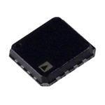
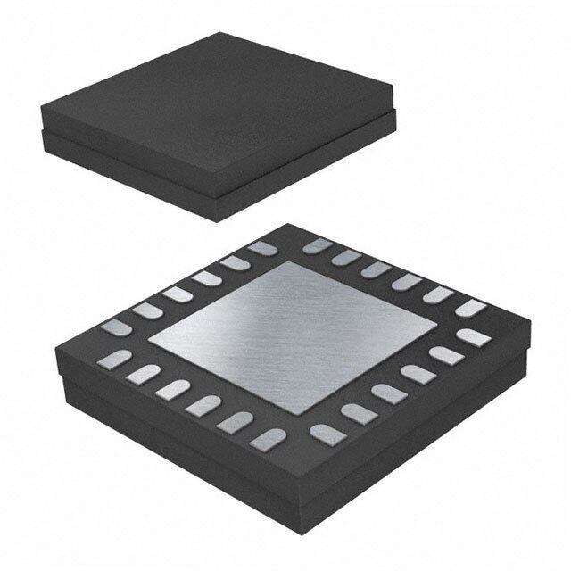
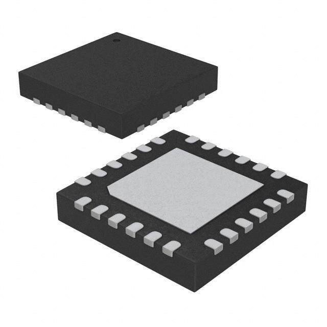
| 供应商器件封装 | 16-LFCSP-VQ (4x4) |
| 其它名称 | ADL5605ACPZ-R7CT |
| 包装 | 剪切带 (CT) |
| 噪声系数 | 4.8dB |
| 增益 | 23dB |
| 封装/外壳 | 16-VQFN 裸露焊盘,CSP |
| 标准包装 | 1 |
| 测试频率 | 943MHz |
| 电压-电源 | 4.75 V ~ 5.25 V |
| 电流-电源 | 307mA |
| 视频文件 | http://www.digikey.cn/classic/video.aspx?PlayerID=1364138032001&width=640&height=505&videoID=2245193150001 |
| 频率 | 700MHz ~ 1GHz |


- 商务部:美国ITC正式对集成电路等产品启动337调查
- 曝三星4nm工艺存在良率问题 高通将骁龙8 Gen1或转产台积电
- 太阳诱电将投资9.5亿元在常州建新厂生产MLCC 预计2023年完工
- 英特尔发布欧洲新工厂建设计划 深化IDM 2.0 战略
- 台积电先进制程称霸业界 有大客户加持明年业绩稳了
- 达到5530亿美元!SIA预计今年全球半导体销售额将创下新高
- 英特尔拟将自动驾驶子公司Mobileye上市 估值或超500亿美元
- 三星加码芯片和SET,合并消费电子和移动部门,撤换高东真等 CEO
- 三星电子宣布重大人事变动 还合并消费电子和移动部门
- 海关总署:前11个月进口集成电路产品价值2.52万亿元 增长14.8%


PDF Datasheet 数据手册内容提取
700 MHz to 1000 MHz, 1 W RF Driver Amplifier Data Sheet ADL5605 FEATURES FUNCTIONAL BLOCK DIAGRAM Operation from 700 MHz to 1000 MHz C C C C N N N N Gain of 23 dB at 943 MHz 6 5 4 3 1 1 1 1 OIP3 of 44.2 dBm at 943 MHz P1dB of 30.9 dBm at 943 MHz RFIN1 12 RFOUT Noise figure of 4.8 dB at 943 MHz DISABLE2 PWDN 11 RFOUT Power supply: 5 V Power supply current: 307 mA typical VCC3 VBIAS 10 RFOUT Internal active biasing VBIAS4 9 RFOUT ADL5605 Fast power-up/power-down function CESoDm rpaatcint g4 omf m±1 × k 4V m (Cmla, s1s6 1-lCe)a d LFCSP C5N C6N C7N C8N 09353-001 Pin-compatible with the ADL5606 (1800 MHz to 2700 MHz) Figure 1. APPLICATIONS Wireless infrastructure Automated test equipment ISM/AMR applications 0 GENERAL DESCRIPTION –10 The ADL5605 is a broadband, two-stage, 1 W RF driver –20 amplifier that operates over a frequency range of 700 MHz to 1000 MHz. –30 c) The ADL5605 operates on a 5 V supply voltage and a supply dB –40 R ( current of 307 mA. The driver also incorporates a fast power- CP –50 A up/power-down function for TDD applications, applications –60 that require a power saving mode, and applications that –70 intermittently transmit data. 946MHz –80 The ADL5605 is fabricated on a GaAs HBT process and is puasecsk aagne edx ipno ase cdo mpapdadclte 4 f omr mex c×e l4l emntm th, 1er6m-leaal dim LpFeCdSaPn cthe.a Tt he –900 2 4 6 8 PO1U0T (d1B2m) 14 16 18 20 22 09353-002 ADL5605 operates from −40°C to +85°C. A fully populated Figure 2. ACPR vs. Output Power, 3GPP, TM1-64, at 946 MHz evaluation board tuned to 943 MHz is also available. Rev. B Document Feedback Information furnished by Analog Devices is believed to be accurate and reliable. However, no responsibility is assumed by Analog Devices for its use, nor for any infringements of patents or other One Technology Way, P.O. Box 9106, Norwood, MA 02062-9106, U.S.A. rights of third parties that may result from its use. Specifications subject to change without notice. No license is granted by implication or otherwise under any patent or patent rights of Analog Devices. Tel: 781.329.4700 ©2011–2017 Analog Devices, Inc. All rights reserved. Trademarks and registered trademarks are the property of their respective owners. Technical Support www.analog.com
ADL5605 Data Sheet TABLE OF CONTENTS Features .............................................................................................. 1 881 MHz Frequency Tuning Band ..............................................9 Applications ....................................................................................... 1 943 MHz Frequency Tuning Band ........................................... 10 General Description ......................................................................... 1 General......................................................................................... 11 Functional Block Diagram .............................................................. 1 Applications Information .............................................................. 13 Revision History ............................................................................... 2 Basic Layout Connections ......................................................... 13 Specifications ..................................................................................... 3 ADL5605 Matching .................................................................... 14 Typical Scattering Parameters ..................................................... 5 ACPR and EVM ......................................................................... 15 Absolute Maximum Ratings ............................................................ 6 Thermal Considerations ............................................................ 15 Thermal Resistance ...................................................................... 6 Soldering Information and Recommended PCB Land ESD Caution .................................................................................. 6 Pattern .......................................................................................... 15 Pin Configuration and Function Descriptions ............................. 7 Evaluation Board ............................................................................ 16 Typical Performance Characteristics ............................................. 8 Outline Dimensions ....................................................................... 18 748 MHz Frequency Tuning Band ............................................. 8 Ordering Guide .......................................................................... 18 REVISION HISTORY 9/2017—Rev. A to Rev. B Changed CP-16-10 to CP-16-20 .................................. Throughout Changes to Figure 1 .......................................................................... 1 Changes to Figure 3 .......................................................................... 7 Updated Outline Dimensions ....................................................... 18 Changes to Ordering Guide .......................................................... 18 11/2013—Rev. 0 to Rev. A Added Figure 29, Renumbered Sequentially .............................. 12 Updated Outline Dimensions ....................................................... 18 7/2011—Revision 0: Initial Version Rev. B | Page 2 of 18
Data Sheet ADL5605 SPECIFICATIONS VCC1 = 5 V and T = 25°C, unless otherwise noted.1 A Table 1. Parameter Test Conditions/Comments Min Typ Max Unit OVERALL FUNCTION Frequency Range 700 1000 MHz FREQUENCY = 748 MHz ± 20 MHz Gain 24.3 dB vs. Frequency ±20 MHz +0.01/−0.19 dB vs. Temperature −40°C ≤ T ≤ +85°C ±0.8 dB A vs. Supply 4.75 V to 5.25 V ±0.07 dB Output 1 dB Compression Point (P1dB) 31.4 dBm vs. Frequency ±20 MHz −0.68/+0.08 dB vs. Temperature −40°C ≤ T ≤ +85°C +0.94/−1.99 dB A vs. Supply 4.75 V to 5.25 V −0.24/−0.05 dB Output Third-Order Intercept (OIP3) ∆f = 1 MHz, P = 14 dBm per tone 41.9 dBm OUT vs. Frequency ±20 MHz −0.22/+0.16 dB vs. Temperature −40°C ≤ T ≤ +85°C +0.07/−1.56 dB A vs. Supply 4.75 V to 5.25 V +0.04/+0.09 dB Noise Figure 4.8 dB FREQUENCY = 881 MHz ± 13 MHz Gain 23.0 dB vs. Frequency ±13 MHz −0.03/−0.08 dB vs. Temperature −40°C ≤ T ≤ +85°C ±0.7 dB A vs. Supply 4.75 V to 5.25 V ±0.05 dB Output 1 dB Compression Point (P1dB) 31.4 dBm vs. Frequency ±13 MHz −0.18/−0.11 dB vs. Temperature −40°C ≤ T ≤ +85°C ±0.6 dB A vs. Supply 4.75 V to 5.25 V −0.4/+0.3 dB Output Third-Order Intercept (OIP3) ∆f = 1 MHz, P = 14 dBm per tone 43.4 dBm OUT vs. Frequency ±13 MHz −0.32/+0.40 dB vs. Temperature −40°C ≤ T ≤ +85°C −0.19/−0.99 dB A vs. Supply 4.75 V to 5.25 V +0.21/−0.03 dB Noise Figure 4.7 dB FREQUENCY = 943 MHz ± 18 MHz Gain 23.0 dB vs. Frequency ±18 MHz +0.28/−0.04 dB vs. Temperature −40°C ≤ T ≤ +85°C ±0.8 dB A vs. Supply 4.75 V to 5.25 V ±0.04 dB Output 1 dB Compression Point (P1dB) 30.9 dBm vs. Frequency ±18 MHz +0.39/−0.08 dB vs. Temperature −40°C ≤ T ≤ +85°C +0.7/−0.9 dB A vs. Supply 4.75 V to 5.25 V −0.43/+0.35 dB Adjacent Channel Power Ratio (ACPR) P = 18 dBm, one-carrier W-CDMA, 51 dBc OUT 64 DPCH, frequency = 946 MHz Output Third-Order Intercept (OIP3) ∆f = 1 MHz, P = 14 dBm per tone 44.2 dBm OUT vs. Frequency ±18 MHz −0.47/−0.10 dB vs. Temperature −40°C ≤ T ≤ +85°C +0.7/−1.6 dB A vs. Supply 4.75 V to 5.25 V −0.08/+0.07 dB Noise Figure 4.8 dB Rev. B | Page 3 of 18
ADL5605 Data Sheet Parameter Test Conditions/Comments Min Typ Max Unit POWER-DOWN INTERFACE DISABLE pin Logic Level to Enable V decreasing 0 1.1 V DISABLE Logic Level to Disable V increasing 1.4 5 V DISABLE DISABLE Pin Current V = 5 V 1.4 mA DISABLE VCC1 Pin Current1 V = 5 V 5.5 mA DISABLE Enable Time 10% of control pulse to 90% of RFOUT 75 ns Disable Time 10% of control pulse to 90% of RFOUT 20 ns POWER INTERFACE RFOUT pin Supply Voltage 4.75 5 5.25 V Supply Current 307 385 mA vs. Temperature −40°C ≤ T ≤ +85°C −20/+1 mA A 1 VCC1 is the supply to the DUT through the RFOUT pins. Rev. B | Page 4 of 18
Data Sheet ADL5605 TYPICAL SCATTERING PARAMETERS VCC1 = 5 V and T = 25°C; the effects of the test fixture have been de-embedded up to the pins of the device.1 A Table 2. Frequency S11 S21 S12 S22 (MHz) Magnitude (dB) Angle (°) Magnitude (dB) Angle (°) Magnitude (dB) Angle (°) Magnitude (dB) Angle (°) 100 −2.38 162.05 5.53 133.84 −48.08 12.48 −1.30 −147.53 150 −2.63 153.17 14.11 95.13 −47.50 2.17 −0.55 −172.43 200 −2.95 144.23 18.99 67.83 −55.96 −119.96 −0.68 −173.81 250 −3.50 135.13 22.75 39.76 −55.27 52.76 −1.24 −171.76 300 −4.41 127.84 25.46 −7.79 −61.09 77.07 −1.10 −176.42 350 −4.58 124.74 23.14 −63.51 −61.80 140.72 −1.06 −177.13 400 −5.11 110.20 17.94 −30.49 −52.49 171.89 −1.15 −176.29 450 −6.82 108.32 22.16 −61.71 −67.98 −27.39 −1.11 −177.02 500 −7.26 106.20 21.56 −87.12 −62.64 −21.99 −0.87 −177.37 550 −7.66 101.35 20.40 −105.19 −61.53 34.70 −0.92 −179.14 600 −8.25 95.77 19.42 −118.96 −61.21 99.93 −0.78 179.80 650 −8.86 89.58 18.55 −130.30 −61.13 129.82 −0.87 179.43 700 −9.58 82.66 17.89 −140.88 −59.03 107.89 −0.87 178.46 750 −10.59 75.33 17.40 −150.63 −61.26 91.70 −0.90 178.01 800 −11.75 66.62 17.07 −160.56 −57.17 92.00 −0.93 177.54 850 −13.27 57.13 16.89 −170.83 −56.35 107.58 −0.93 177.22 900 −15.44 46.13 16.84 178.03 −56.74 99.86 −0.96 176.90 950 −18.94 29.27 16.93 165.27 −54.82 107.20 −0.96 176.66 1000 −26.34 −2.06 16.96 150.36 −52.26 73.48 −0.98 176.43 1050 −26.92 −130.02 16.77 132.88 −54.70 68.96 −0.94 176.27 1100 −18.87 −171.63 16.17 113.62 −54.77 47.54 −0.81 176.15 1150 −15.30 163.88 14.89 94.11 −53.44 43.95 −0.76 175.49 1200 −13.83 145.18 13.13 76.86 −55.60 11.97 −0.72 174.79 1250 −13.51 129.85 11.09 62.33 −55.37 33.66 −0.66 173.83 1300 −13.68 117.81 8.95 50.66 −57.24 20.12 −0.68 173.19 1350 −14.26 108.51 6.91 41.54 −59.07 24.50 −0.66 172.57 1400 −14.96 99.61 4.91 33.49 −60.44 14.20 −0.69 171.85 1450 −15.76 92.58 3.04 26.87 −61.45 45.66 −0.63 171.46 1500 −16.83 86.52 1.23 21.09 −57.41 62.21 −0.69 170.87 1550 −17.90 79.79 −0.47 16.01 −62.00 53.37 −0.66 170.42 1600 −19.28 73.87 −2.09 11.40 −56.83 57.90 −0.69 169.98 1650 −20.56 67.65 −3.63 7.32 −57.60 58.62 −0.68 169.51 1700 −22.42 60.60 −5.10 3.62 −59.47 77.96 −0.68 168.99 1750 −24.45 51.72 −6.53 0.23 −58.70 76.85 −0.67 168.59 1800 −26.42 38.39 −7.92 −3.05 −55.11 66.53 −0.68 168.10 1850 −28.73 21.43 −9.27 −6.05 −58.19 37.40 −0.67 167.72 1900 −29.99 −4.11 −10.56 −8.66 −61.08 43.12 −0.68 167.18 1950 −29.61 −32.34 −11.84 −11.11 −57.28 78.91 −0.67 166.94 2000 −27.80 −55.73 −13.07 −13.38 −56.29 83.05 −0.68 166.45 1 VCC1 is the supply to the DUT through the RFOUT pins. Rev. B | Page 5 of 18
ADL5605 Data Sheet ABSOLUTE MAXIMUM RATINGS THERMAL RESISTANCE Table 3. Parameter Rating Table 4 lists the junction-to-air thermal resistance (θ ) and the JA Supply Voltage, VCC11 6.5 V junction-to-paddle thermal resistance (θJC) for the ADL5605. Input Power (50 Ω Impedance) 20 dBm For more information, see the Thermal Considerations section. Internal Power Dissipation (Paddle Soldered) 2 W Table 4. Thermal Resistance Maximum Junction Temperature 150°C Package Type θ θ Unit Lead Temperature (Soldering 60 sec) 240°C JA JC 16-Lead LFCSP (CP-16-20) 52.1 12.1 °C/W Operating Temperature Range −40°C to +85°C Storage Temperature Range −65°C to +150°C 1 VCC1 is the supply to the DUT through the RFOUT pins. ESD CAUTION Stresses at or above those listed under Absolute Maximum Ratings may cause permanent damage to the product. This is a stress rating only; functional operation of the product at these or any other conditions above those indicated in the operational section of this specification is not implied. Operation beyond the maximum operating conditions for extended periods may affect product reliability. Rev. B | Page 6 of 18
Data Sheet ADL5605 PIN CONFIGURATION AND FUNCTION DESCRIPTIONS C C C C N N N N 6 5 4 3 1 1 1 1 RFIN 1 12 RFOUT DISABLE 2 ADL5605 11 RFOUT TOP VIEW VCC 3 (Not to Scale) 10 RFOUT VBIAS 4 9 RFOUT 5 6 7 8 C C C C N N N N NOTES 1.NC = NO CONNECT. DO NOT CONNECT TO THIS PIN. 2.TAGH RLEOO UEWXN PIDMO PPSLEEADDNA EPN.ACDED ELLEE SCHTORIUCLADL BAEN DSO TLHDEERRMEADL TO 09353-003 Figure 3. Pin Configuration Table 5. Pin Function Descriptions Pin No. Mnemonic Description 1 RFIN RF Input. Requires a dc blocking capacitor. 2 DISABLE Connect this pin to 5 V to disable the part. In the disabled state, the part draws approximately 5 mA of current from the power supply and 1.4 mA from the DISABLE pin. 3 VCC Under normal operation, this pin is connected to the power supply and draws a combined 307 mA of current. When this pin is grounded along with the VBIAS pin, the device is disabled and draws approximately 1.4 mA from the DISABLE pin. 4 VBIAS Applying 5 V to this pin enables the bias circuit. When this pin is grounded, the device is disabled. 5, 6, 7, 8, 13, NC No Connect. Do not connect to this pin. 14, 15, 16 9, 10, 11, 12 RFOUT RF Output. DC bias is provided to this pin through an inductor that is connected to the 5 V power supply. The RF path requires a dc blocking capacitor. EP The exposed paddle should be soldered to a low impedance electrical and thermal ground plane. Rev. B | Page 7 of 18
ADL5605 Data Sheet TYPICAL PERFORMANCE CHARACTERISTICS 748 MHZ FREQUENCY TUNING BAND 50 42 46 Bm) 45 OIP3 (dBm) 40 –40°C 44 d dB, 40 38 42 3 ( +25°C P 35 OI P1dB (dBm) 36 +85°C 40 N, P1dB, 3205 GAIN (dB) B (dBm) 34 –40°C 38 3 (dBm) GAI 20 P1d 32 36 OIP URE, 15 30 +25°C 34 E FIG 10 28 +85°C 32 S NF (dB) NOI 5 26 30 0728 733 738 F74R3EQUE7N4C8Y (M7H5z3) 758 763 768 09353-004 24728 733 738 F74R3EQUE7N4C8Y (M7H5z3) 758 763 76828 09353-007 Figure 4. Noise Figure, Gain, P1dB, and OIP3 vs. Frequency Figure 7. P1dB and OIP3 vs. Frequency and Temperature (OIP3 at POUT = 14 dBm per Tone) (OIP3 at POUT = 14 dBm per Tone) 28 44 27 43 768MHz 26 –40°C 42 748MHz 25 B) +25°C m) d B 728MHz AIN ( 24 +85°C P3 (d 41 G OI 23 40 22 39 21 20728 733 738 F74R3EQUE7N4C8Y (M7H5z3) 758 763 768 09353-005 38–2 0 2 4POUT6 PER T8ONE 1(d0Bm)12 14 16 18 09353-008 Figure 5. Gain vs. Frequency and Temperature Figure 8. OIP3 vs. POUT and Frequency 0 7 S22 –10 6 S11 ETERS (dB) ––2300 GURE (dB) 5 ++8255°°CC M FI S-PARA –40 NOISE 4 –40°C 3 –50 S12 –60728 733 738 F74R3EQUE7N4C8Y (M7H5z3) 758 763 768 09353-006 2728 738 FREQUE7N4C8Y (MHz) 758 768 09353-009 Figure 6. Input Return Loss (S11), Output Return Loss (S22), Figure 9. Noise Figure vs. Frequency and Temperature and Reverse Isolation (S12) vs. Frequency Rev. B | Page 8 of 18
Data Sheet ADL5605 881 MHZ FREQUENCY TUNING BAND 50 40 46 m) OIP3 (dBm) +25°C B 45 d 38 44 B, 40 d P3 ( 35 36 –40°C +85°C 42 OI P1dB (dBm) N, P1dB, 3205 GAIN (dB) B (dBm) 34 –40°C +25°C 40 3 (dBm) GAI 20 P1d 32 38 OIP E, R U 15 30 +85°C 36 G E FI 10 S NF (dB) 28 34 NOI 5 0868 873 F8R7E8QUENCY8 (8M3Hz) 888 893 09353-010 26868 870 872 874 876F8R7E8Q8U8E0NC88Y2 (M8H84z)886 888 890 892 89432 09353-013 Figure 10. Noise Figure, Gain, P1dB, and OIP3 vs. Frequency Figure 13. P1dB and OIP3 vs. Frequency and Temperature (OIP3 at POUT = 14 dBm per Tone) (OIP3 at POUT = 14 dBm per Tone) 27 45 26 894MHz 44 881MHz 25 43 24 –40°C 868MHz B) m) d +25°C B AIN ( 23 +85°C P3 (d 42 G OI 22 41 21 40 20 19868 870 872 874 876F8R7E8Q8U8E0NC88Y2 (M8H84z)886 888 890 892 894 09353-011 39–2 0 2 4POUT6 PER T8ONE 1(d0Bm)12 14 16 18 09353-014 Figure 11. Gain vs. Frequency and Temperature Figure 14. OIP3 vs. POUT and Frequency 0 7 S22 –10 S11 6 ETERS (dB) ––2300 GURE (dB) 5 ++2855°°CC M FI –40°C S-PARA –40 NOISE 4 S12 3 –50 –60868 873 F8R7E8QUENCY8 (8M3Hz) 888 893 09353-012 2868 F8R7E8QUENCY (MHz) 888 09353-015 Figure 12. Input Return Loss (S11), Output Return Loss (S22), Figure 15. Noise Figure vs. Frequency and Temperature and Reverse Isolation (S12) vs. Frequency Rev. B | Page 9 of 18
ADL5605 Data Sheet 943 MHZ FREQUENCY TUNING BAND 50 40 48 Bm) 45 OIP3 (dBm) B, d 40 38 –40°C +25°C 46 d P3 ( 35 36 44 OI P1dB (dBm) +85°C 1dB, 30 Bm) 34 42 Bm) N, P 25 GAIN (dB) B (d 3 (d GAI 20 P1d 32 –40°C +25°C 40 OIP E, UR 15 30 38 G E FI 10 +85°C NOIS 5 NF (dB) 28 36 0925 930 935 FRE9Q40UENCY9 4(M5Hz) 950 955 960 09353-016 26925 930 935 FRE9Q40UENCY9 4(M5Hz) 950 955 96034 09353-019 Figure 16. Noise Figure, Gain, P1dB, and OIP3 vs. Frequency Figure 19. P1dB and OIP3 vs. Frequency and Temperature (OIP3 at POUT = 14 dBm per Tone) (OIP3 at POUT = 14 dBm per Tone) 27 46 26 45 943MHz 25 B) 24 –40°C m) 44 960MHz 925MHz GAIN (d 23 ++8255°°CC OIP3 (dB 43 22 42 21 41 20 19925 930 935 FRE9Q40UENCY9 4(M5Hz) 950 955 960 09353-017 40–2 0 2 4POUT6 PER T8ONE 1(d0Bm)12 14 16 18 09353-020 Figure 17. Gain vs. Frequency and Temperature Figure 20. OIP3 vs. POUT and Frequency 0 7 S22 –10 6 S11 ETERS (dB) ––2300 GURE (dB) 5 ++8255°°CC M FI –40°C S-PARA –40 NOISE 4 S12 3 –50 –60925 930 935 FRE9Q40UENCY9 4(M5Hz) 950 955 960 09353-018 2925 930 935 FRE9Q40UENCY9 4(M5Hz) 950 955 960 09353-021 Figure 18. Input Return Loss (S11), Output Return Loss (S22), Figure 21. Noise Figure vs. Frequency and Temperature and Reverse Isolation (S12) vs. Frequency Rev. B | Page 10 of 18
Data Sheet ADL5605 GENERAL 35 35 30 30 25 25 %) %) GE ( 20 GE ( 20 A A T T N N CE 15 CE 15 R R E E P P 10 10 5 5 0 43.7 43.8 43.9 44.0 44.1O4I4P.32 (d44B.m3)44.4 44.5 44.6 44.7 44.8 09353-022 0 4.45 4.50 4.55NOIS4.E6 0FIGU4R.6E5 (dB)4.70 4.75 4.80 09353-025 Figure 22. OIP3 Distribution at 943 MHz, 14 dBm per Tone Figure 25. Noise Figure Distribution at 943 MHz 40 0 35 –10 –20 30 %) –30 E ( 25 c) G B –40 PERCENTA 1250 ACPR (d ––5600 10 –70 946MHz 5 –80 030.5 30.6 30.7 30.8 30P.91dB31 (.d0Bm31).1 31.2 31.3 31.4 31.5 09353-023 –900 2 4 6 8 PO1U0T (d1B2m) 14 16 18 20 22 09353-026 Figure 23. P1dB Distribution at 943 MHz Figure 26. ACPR vs. POUT, 3GPP, TM1-64, at 946 MHz 40 3.5 35 3.0 30 2.5 %) GE ( 25 %) 2.0 TA 20 M ( N V CE E 1.5 ER 15 P 1.0 10 946MHz 0.5 5 0 22.7 22.8 22.9 2G3.A0IN (d2B3.)1 23.2 23.3 23.4 09353-024 0–10 –5 0 P5OUT (dBm10) 15 20 25 09353-027 Figure 24. Gain Distribution at 943 MHz Figure 27. EVM vs. POUT, 3GPP, TM1-64, at 946 MHz Rev. B | Page 11 of 18
ADL5605 Data Sheet 320 5.25V 310 5V A) m T ( 4.75V N E R R 300 U C 3 Y L P P U S 290 2 280–40 –30 –20 –10 0TE1M0PER2A0TU3R0E (°4C0) 50 60 70 80 09353-028 CH3 1V Ω CH2 1V Ω AM 2 C0nHs2 1 0 G 2S.5/sV IT 4ps/pt 09353-029 Figure 28. Supply Current vs. Temperature and Supply Voltage at 943 MHz Figure 30. Turn-Off Time, 10% of Control Pulse to 90% of RFOUT 860 +25°C 760 A) m T ( 660 N E R R U 560 C Y 3 L P UP 460 S 360 +85°C 2 –40°C 260–6–4–2 0 2 4 6 8 10P1O2UT1 4(d1B6m1)82022242628303234 09353-100 CH3 1V Ω CH2 1V Ω AM 2 C0nHs2 1 0 G 2S.5/sV IT 4ps/pt 09353-030 Figure 29. Supply Current vs. POUT and Temperature at 943 MHz, VCC = 5 V Figure 31. Turn-On Time, 10% of Control Pulse to 90% of RFOUT Rev. B | Page 12 of 18
Data Sheet ADL5605 APPLICATIONS INFORMATION BASIC LAYOUT CONNECTIONS For complete information about component values and spacing for the different frequency tuning bands, see the ADL5605 The basic connections for operating the ADL5605 are shown Matching section. in Figure 32. The RF matching components correspond to the 943 MHz frequency tuning band. RF Output Interface Power Supply Pin 9 to Pin 12 are the RF output pins. Inductor L2, the shunt capacitor, C , and the inductance from the microstrip line are The voltage supply for the ADL5605, which ranges from 4.75 V OUT used to match the RF output to 50 Ω. For complete information to 5.25 V, should be connected to the VCC1 test pin. The dc bias about component values and spacing for the different frequency to the output stage is supplied through L1 and is connected to the tuning bands, see the ADL5605 Matching section. RFOUT pin. Three decoupling capacitors (C7, C8, and C9) are used to prevent RF signals from propagating on the dc lines. The Power-Down VBIAS and VCC pins can be directly connected to the main The ADL5605 can be disabled by connecting the DISABLE pin supply voltage. Additional decoupling capacitors (C5, C6, C11, to 5 V. When disabled, the ADL5605 draws approximately 5 mA C12, C13, and C14) are required on the VCC and VBIAS pins. of current from the power supply and 1.4 mA from the DISABLE RF Input Interface pin. Decoupling Capacitor C3 is recommended to prevent the propagation of RF signals. To completely shut down the device, Pin 1 is the RF input pin for the ADL5605. The RF input is easily connect the VCC pin, the VBIAS pin, and the VCC1 test pin to matched to 50 Ω with only one shunt capacitor and the micro- ground. In this state, the part draws approximately 1.4 mA from strip line used as an inductor. For the 881 MHz and 943 MHz the DISABLE pin. frequency tuning bands, the input requires no external matching components. 16 15 14 13 C1 RFIN 100pF NC NC NC NC 1 RFIN RFOUT 12 COUT C2 2 DISABLE RFOUT 11 8pF 100pF RFOUT ADL5605 3 VCC RFOUT 10 L2 DISABLE C3 L1 1.6nH 10pF 4 VBIAS RFOUT 9 18nH NC NC NC NC C7 VCC C11 C6 C5 5 6 7 8 100pF 10µF 0.01µF 100pF C8 0.01µF VBIAS C14 C13 C12 10µF 0.01µF 100pF C9 10µF VCC1 09353-031 Figure 32. Basic Connections Rev. B | Page 13 of 18
ADL5605 Data Sheet ADL5605 MATCHING Figure 33 to Figure 35 show the matching networks. The RF input of the ADL5605 can be easily matched to 50 Ω Table 6. Recommended Components for Basic Connections with at most one external component and the microstrip line Frequency (MHz) C (pF) L2 (nH) C (pF) IN OUT used as an inductor. The RF output requires one series inductor, 728 to 768 2.4 2.7 12.0 one shunt capacitor, and the microstrip line used as an inductor. 868 to 894 N/A 1.6 8.0 Table 6 lists the required matching component values. Capac- 925 to 961 N/A 1.6 8.0 itors C and C are Murata GRM155 series (0402 size), and IN OUT Inductor L2 is a Coilcraft® 0603CS series (0603 size). Table 7. Matching Component Spacing For all frequency tuning bands, the placement of C , L2, and IN Frequency (MHz) λ1 (mils) λ2 (mils) λ3 (mils) C is critical. Table 7 lists the recommended component OUT 728 to 768 63 94.5 169 spacing for the various frequency tuning bands. The component 868 to 894 N/A 94.5 268 spacing is referenced from the center of the component to the edge of the package. 925 to 961 N/A 94.5 240 16 15 14 13 RFIN 10C01pF NC NC NC NC 1 RFIN RFOUT 12 CIN λ1 2.4pF 2 DISABLE RFOUT 11 λ3 C12OpUFT RFOUT ADL5605 RFOUT 10 λ2 2.L7n2H 10C02pF RFOUT 9 L1 18nH 09353-032 Figure 33. ADL5605 Match Parameters, 748 MHz Frequency Tuning Band 16 15 14 13 RFIN 10C01pF NC NC NC NC 1 RFIN RFOUT 12 CIN OPEN 2 DISABLE RFOUT 11 λ3 C8pOFUT RFOUT ADL5605 RFOUT 10 λ2 1.L6n2H 10C02pF RFOUT 9 L1 18nH 09353-033 Figure 34. ADL5605 Match Parameters, 881 MHz Frequency Tuning Band 16 15 14 13 RFIN 10C01pF NC NC NC NC 1 RFIN RFOUT 12 CIN OPEN 2 DISABLE RFOUT 11 λ3 C8pOFUT RFOUT ADL5605 RFOUT 10 λ2 1.L6n2H 10C02pF RFOUT 9 L1 18nH 09353-034 Figure 35. ADL5605 Match Parameters, 943 MHz Frequency Tuning Band Rev. B | Page 14 of 18
Data Sheet ADL5605 ACPR AND EVM For optimal performance, it is recommended that the thermal vias be filled with a conductive paste of the equivalent thermal All adjacent channel power ratio (ACPR) and error vector conductivity specified earlier in this section; alternatively, an magnitude (EVM) measurements were made using a single external heat sink can be used to dissipate heat quickly without W-CDMA carrier and Test Model 1-64. affecting the die junction temperature. It is also recommended The signal is generated by a very low ACPR source and is meas- that the ground pattern be extended above and below the device ured at the output by a high dynamic range spectrum analyzer. to improve thermal efficiency (see Figure 36). For ACPR measurements, the filter setting was chosen for low SOLDERING INFORMATION AND RECOMMENDED ACPR; for EVM measurements, the low EVM setting was selected. PCB LAND PATTERN The spectrum analyzer incorporates an instrument noise correc- tion function, and highly linear amplifiers were used to boost Figure 36 shows the recommended land pattern for the ADL5605. the power levels for ACPR measurements. To minimize thermal impedance, the exposed paddle on the 4 mm × 4 mm LFCSP is soldered to a ground plane along with Figure 26 shows ACPR vs. P at 946 MHz. For power levels OUT Pin 5 to Pin 8 and Pin 13 to Pin 16. To improve thermal dissi- up to 18 dBm, an ACPR of 51 dBc or better can be achieved pation, 25 thermal vias are arranged in a 5 × 5 array under the at 946 MHz. exposed paddle. Areas above and below the paddle are tied with Figure 27 shows EVM vs. P at 946 MHz. The EVM measured OUT regular vias. If multiple ground layers exist, they should be tied is 0.5% for power levels up to 18 dBm at 946 MHz. The baseline together using vias. For more information about land pattern composite EVM for the signal source was approximately 0.5%. design and layout, see the AN-772 Application Note, A Design When operated in the linear region, there is little or no contribu- and Manufacturing Guide for the Lead Frame Chip Scale Package tion to EVM by the amplifier. (LFCSP). THERMAL CONSIDERATIONS The ADL5605 is packaged in a thermally efficient 4 mm × 4 mm, 16-lead LFCSP. The thermal resistance from junction to air (θ ) is 52.1°C/W. The thermal resistance for the product JA was extracted assuming a standard 4-layer JEDEC board with 25 copper plated thermal vias. The thermal vias are filled with 16 13 conductive copper paste (AE3030 with thermal conductivity of 7.8 W/mK and thermal expansion α1 of 4 × 10⁻⁵/°C and α2 of RFIN 8.6 × 10⁻⁵/°C). The thermal resistance from junction to case (θ ) JC RFOUT is 12.1°C/W, where the case is the exposed pad of the lead frame 16 MIL VIA PAD WITH 8 MIL VIA package. For the best thermal performance, it is recommended that as 5 8 many thermal vias as possible be added under the exposed pad of the LFCSP. The thermal resistance values assume a minimum of 25 thermal vias arranged in a 5 × 5 array with a via diameter of 8 mils, via pad of 16 mils, and a pitch of 20 mils. The vias are plated with copper, and the drill hole is filled with a conductive c opper paste. 09353-035 Figure 36. Recommended Land Pattern Rev. B | Page 15 of 18
ADL5605 Data Sheet EVALUATION BOARD The schematic of the ADL5605 evaluation board is shown in The evaluation board has a short, non-50 Ω line on its output Figure 37. The evaluation board uses 25 mils wide, 50 Ω traces to accommodate the four output pins and to allow for easier low and is made from IS410 material with a 20 mils gap to ground. inductance output matching. The pads for Pin 9 to Pin 12 are The evaluation board is tuned for operation at 943 MHz. The included on this microstrip line and are included in all matches. inputs and outputs should be ac-coupled with appropriately The evaluation board uses numbers as identifiers to aid in the sized capacitors; therefore, for low frequency applications, the placement of matching components at both the RF input and value of C1 and C2 may need to be increased. DC bias is RF output of the device. Figure 38 and Figure 39 show images provided to the output stage via an inductor (L1) connected of the board layout. to the RFOUT pin. A bias voltage of 5 V is recommended. 16 15 14 13 C1 RFIN 100pF NC NC NC NC 1 RFIN RFOUT 12 CIN COUT C2 N/A 2 DISABLE RFOUT 11 8pF 100pF RFOUT ADL5605 3 VCC RFOUT 10 L2 DISABLE C10 C4 C3 L1 1.6nH OPEN OPEN 10pF 4 VBIAS RFOUT 9 18nH R4 OPEN NC NC NC NC C7 VCC3 C11 C6 C5 5 6 7 8 100pF 10µF 0.01µF 100pF C8 0RΩ1 VCC2 0.01µF R5 C14 C13 C12 C9 OPEN 10µF 0.01µF 100pF 10µF 0RΩ2 VCC1 09353-036 Figure 37. Evaluation Board, 943 MHz Frequency Tuning Band Table 8. Evaluation Board Configuration Options, 943 MHz Frequency Tuning Band Component Function/Notes Default Value C1, C2 Input/output dc blocking capacitors. C1, C2 = 100 pF C3, C4, C5, C6, C7, Power supply decoupling capacitors. Power supply decoupling capacitors are required to C3 = 10 pF C8, C9, C10, C11, filter out the high frequency noise on the power supply. The smallest capacitor should be the C5, C7, C12 = 100 pF C12, C13, C14 closest to the ADL5605. The main bias that goes through RFOUT is the most sensitive to noise C6, C8, C13 = 0.01 µF because the bias is connected directly to the RF output. C9, C11, C14 = 10 µF C4, C10 = open C Input matching capacitor. To match the ADL5605 at the 943 MHz or 881 MHz frequency tuning C = open IN IN band, C is not required. For the 748 MHz frequency tuning band, C is set at a specific distance IN IN from the device so that the microstrip line can act as inductance for the matching network (see Table 7). If space is at a premium, an inductor can take the place of the microstrip line. C Output matching capacitor. The output match is set for 943 MHz and is easily changed for C = 8.0 pF HQ OUT OUT other frequency tuning bands. The tolerance of this capacitor should be tight. C is set at OUT a specific distance from the device so that the microstrip line can act as inductance for the matching network (see Table 7). If space is at a premium, an inductor can take the place of the microstrip line. A short length of low impedance line on the output is embedded in the match. L2 Output matching inductor. The output match is set for 943 MHz and is easily changed for other L2 = 1.6 nH HQ frequency tuning bands. A high Q Coilcraft inductor with tight tolerance is recommended. L1 The main bias for the ADL5605 comes through L1 to the output stage. L1 should be high L1 = 18 nH impedance for the frequency of operation while providing low resistance for the dc current. The evaluation board uses a Coilcraft 0603HP-18NX_LU inductor; this 18 nH inductor provides some of the match at 943 MHz. R1, R2, R4, R5 To provide bias to all stages through just one supply, set R1 and R2 to 0 Ω, and leave R4 and R1, R2 = 0 Ω R5 open. To provide separate bias to stages, set R1 and R2 to open and R4 and R5 to 0 Ω. R4, R5 = open Exposed Paddle The paddle should be connected to both thermal and electrical ground. Rev. B | Page 16 of 18
Data Sheet ADL5605 09353-037 09353-038 Figure 38. Evaluation Board Layout, Top Figure 39. Evaluation Board Layout, Bottom Rev. B | Page 17 of 18
ADL5605 Data Sheet OUTLINE DIMENSIONS DETAIL A (JEDEC 95) 4.10 0.35 4.00 SQ 0.30 PIN 1 3.90 0.25 INDICATOR 0.65 13 16 PI(NSINDE EI1C DAETTAOIRL AAR)EA OPTIONS BSC 12 1 *2.40 EXPPAODSED 2.35 SQ 2.30 9 4 0.50 8 5 0.25 MIN TOP VIEW 0.40 BOTTOM VIEW 0.30 0.80 FOR PROPER CONNECTION OF 0.75 SIDE VIEW THE EXPOSED PAD, REFER TO 0.05 MAX THE PIN CONFIGURATION AND 0.70 0.02 NOM FUNCTION DESCRIPTIONS COPLANARITY SECTION OF THIS DATA SHEET. SEATING 0.08 PKG-004024 PLANE *CWOITMHP ELIXACNETPTTOIOJNE DT0EO.C2 T0 SH RTEEA EFNXDPAORSDESD M POA-D2.20-WGGC-3 03-30-2017-B Figure 40. 16-Lead Lead Frame Chip Scale Package [LFCSP] 4 mm × 4 mm Body and 0.75 mm Package Height (CP-16-20) Dimensions shown in millimeters ORDERING GUIDE Model1 Temperature Range Package Description Package Option ADL5605ACPZ-R7 −40°C to +85°C 16-Lead Lead Frame Chip Scale Package [LFCSP] CP-16-20 ADL5605-EVALZ Evaluation Board 1 Z = RoHS Compliant Part. ©2011–2017 Analog Devices, Inc. All rights reserved. Trademarks and registered trademarks are the property of their respective owners. D09353-0-9/17(B) Rev. B | Page 18 of 18
Mouser Electronics Authorized Distributor Click to View Pricing, Inventory, Delivery & Lifecycle Information: A nalog Devices Inc.: ADL5605ACPZ-R7 ADL5605-EVALZ