ICGOO在线商城 > 射频/IF 和 RFID > RF 放大器 > ADL5601ARKZ-R7
 Datasheet下载
- 型号: ADL5601ARKZ-R7
- 制造商: Analog
- 库位|库存: xxxx|xxxx
- 要求:
| 数量阶梯 | 香港交货 | 国内含税 |
| +xxxx | $xxxx | ¥xxxx |
查看当月历史价格
查看今年历史价格
ADL5601ARKZ-R7产品简介:
ICGOO电子元器件商城为您提供ADL5601ARKZ-R7由Analog设计生产,在icgoo商城现货销售,并且可以通过原厂、代理商等渠道进行代购。 ADL5601ARKZ-R7价格参考¥13.96-¥14.47。AnalogADL5601ARKZ-R7封装/规格:RF 放大器, 射频放大器 IC 通用 50MHz ~ 4GHz SOT-89-3。您可以下载ADL5601ARKZ-R7参考资料、Datasheet数据手册功能说明书,资料中有ADL5601ARKZ-R7 详细功能的应用电路图电压和使用方法及教程。
ADL5601ARKZ-R7 是由 Analog Devices Inc. 生产的一款 RF 放大器,专为高性能、低噪声和高线性度的应用而设计。其主要应用场景包括无线通信系统、测试与测量设备、以及各种射频前端模块。

 1. 无线通信系统
在无线通信领域,ADL5601ARKZ-R7 可用于基站、中继站和其他无线基础设施设备中。它能够提供稳定的增益和低噪声特性,确保信号传输的高质量。特别是在蜂窝网络(如4G LTE和5G)中,该放大器可以有效提升信号覆盖范围和数据传输速率,同时减少干扰和失真。

 2. 测试与测量设备
对于需要精确测量射频信号的仪器,如频谱分析仪、矢量网络分析仪等,ADL5601ARKZ-R7 的低噪声系数和高线性度使其成为理想选择。它可以提高测量精度,确保测试结果的可靠性。此外,该放大器还具有宽频带响应,适用于多种频率范围内的测试需求。

 3. 射频前端模块
在射频前端模块中,ADL5601ARKZ-R7 可以作为低噪声放大器(LNA)或驱动放大器使用。它能够在接收链路中增强微弱信号,确保信号不失真地传输到后续处理单元。同时,在发射链路中,该放大器可以提供足够的驱动功率,确保信号的有效发送。

 4. 卫星通信和雷达系统
ADL5601ARKZ-R7 还广泛应用于卫星通信和雷达系统中。其高线性度和低噪声特性有助于提高系统的灵敏度和分辨率,从而实现更远距离和更清晰的目标探测。在卫星通信中,该放大器可以帮助克服长距离传输中的信号衰减问题,确保数据传输的稳定性和可靠性。

总之,ADL5601ARKZ-R7 凭借其卓越的性能,适用于多种需要高性能射频信号处理的场合,是现代通信和测量系统中的关键组件之一。
| 参数 | 数值 |
| 产品目录 | |
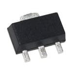
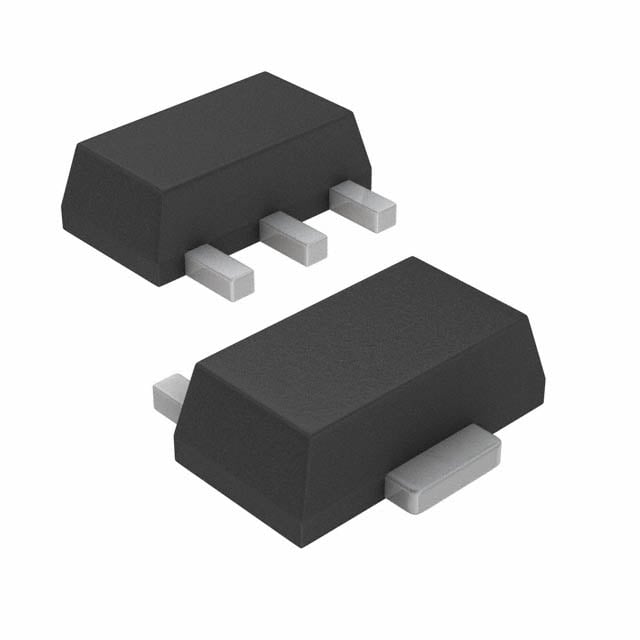
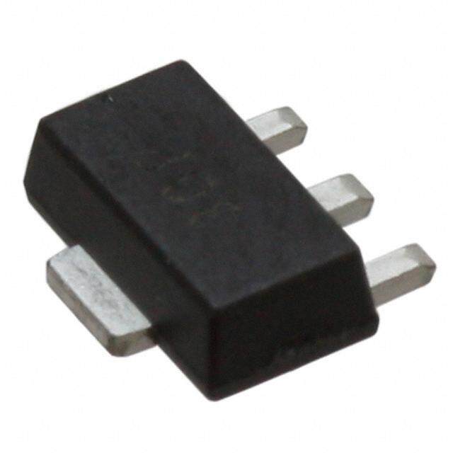
| 描述 | IC AMP GAIN BLOCK 15DB SOT89-3射频放大器 50MHz-4.0GHz RF/IF Gain Block |
| DevelopmentKit | ADL5601-EVALZ |
| 产品分类 | |
| 品牌 | Analog Devices Inc |
| 产品手册 | |
| 产品图片 |
|
| rohs | 符合RoHS无铅 / 符合限制有害物质指令(RoHS)规范要求 |
| 产品系列 | RF集成电路,射频放大器,Analog Devices ADL5601ARKZ-R7- |
| 数据手册 | |
| P1dB | 19dB(79.4mW) |
| 产品型号 | ADL5601ARKZ-R7 |
| RF类型 | 通用 |
| 产品目录页面 | |
| 产品种类 | 射频放大器 |
| 供应商器件封装 | SOT-89-3 |
| 其它名称 | ADL5601ARKZ-R7CT |
| 功率增益类型 | 15.3 dB |
| 包装 | 剪切带 (CT) |
| 商标 | Analog Devices |
| 噪声系数 | 3.7dB |
| 增益 | 15dB |
| 安装风格 | SMD/SMT |
| 封装 | Reel |
| 封装/外壳 | TO-243AA |
| 封装/箱体 | SOT-89-3 |
| 工作电源电压 | 5 V |
| 工作频率 | 50 MHz to 4000 MHz |
| 工厂包装数量 | 1000 |
| 最大功率耗散 | 600 mW |
| 最大工作温度 | + 85 C |
| 最小工作温度 | - 40 C |
| 标准包装 | 1 |
| 测试频率 | 900MHz |
| 特色产品 | http://www.digikey.com/cn/zh/ph/analog-devices/adl560x.html |
| 电压-电源 | 4.5 V ~ 5.5 V |
| 电流-电源 | 83mA |
| 电源电流 | 83 mA |
| 类型 | Gain Block Amplifier |
| 系列 | ADL5601 |
| 视频文件 | http://www.digikey.cn/classic/video.aspx?PlayerID=1364138032001&width=640&height=505&videoID=2245193150001 |
| 输出截获点 | 43 dBm |
| 通道数量 | 1 Channel |
| 隔离分贝 | - 20 dB |
| 频率 | 50MHz ~ 4GHz |


- 商务部:美国ITC正式对集成电路等产品启动337调查
- 曝三星4nm工艺存在良率问题 高通将骁龙8 Gen1或转产台积电
- 太阳诱电将投资9.5亿元在常州建新厂生产MLCC 预计2023年完工
- 英特尔发布欧洲新工厂建设计划 深化IDM 2.0 战略
- 台积电先进制程称霸业界 有大客户加持明年业绩稳了
- 达到5530亿美元!SIA预计今年全球半导体销售额将创下新高
- 英特尔拟将自动驾驶子公司Mobileye上市 估值或超500亿美元
- 三星加码芯片和SET,合并消费电子和移动部门,撤换高东真等 CEO
- 三星电子宣布重大人事变动 还合并消费电子和移动部门
- 海关总署:前11个月进口集成电路产品价值2.52万亿元 增长14.8%


PDF Datasheet 数据手册内容提取
50 MHz to 4.0 GHz RF/IF Gain Block Data Sheet ADL5601 FEATURES FUNCTIONAL BLOCK DIAGRAM Fixed gain of 15 dB GND Operation from 50 MHz to 4.0 GHz (2) Highest dynamic range gain block ADL5601 Input/output internally matched to 50 Ω Integrated bias control circuit BIAS OIP3 of 43.0 dBm at 900 MHz PN1odisBe ofifg 1u9r.e0 odfB 3m.7 a dtB 9 a0t0 9 M0H0 zM Hz RF1IN GN2D RFO3UT 08219-001 Single 5 V power supply Figure 1. Low quiescent current of 83 mA Thermally efficient SOT-89 package ESD rating of ±1.5 kV (Class 1C) GENERAL DESCRIPTION The ADL5601 is a broadband, 15 dB linear amplifier that operates variety of applications. Only input/output ac coupling capacitors, at frequencies up to 4.0 GHz. The device can be used in a wide power supply decoupling capacitors, and an external inductor variety of cellular, cable television (CATV), military, and instru- are required for operation. mentation equipment. The ADL5601 is fabricated on an InGaP heterojunction bipolar The ADL5601 provides the highest dynamic range available transistor (HBT) process and has an ESD rating of ±1.5 kV from an internally matched gain block. This is accomplished by (Class 1C). The device is available in a thermally efficient SOT-89 providing extremely low noise figures and very high OIP3 speci- package. fications simultaneously, across the entire 4.0 GHz frequency range. The ADL5601 consumes 83 mA on a single 5 V supply and is The ADL5601 provides a gain of 15 dB, which is stable over fully specified for operation from −40°C to +85°C. frequency, temperature, and supply voltage, as well as from device A fully populated RoHS-compliant evaluation board is to device. The device is internally matched to 50 Ω at the input available. and output, making the ADL5601 very easy to implement in a wide Rev. A Document Feedback Information furnished by Analog Devices is believed to be accurate and reliable. However, no responsibility is assumed by Analog Devices for its use, nor for any infringements of patents or other One Technology Way, P.O. Box 9106, Norwood, MA 02062-9106, U.S.A. rights of third parties that may result from its use. Specifications subject to change without notice. No license is granted by implication or otherwise under any patent or patent rights of Analog Devices. Tel: 781.329.4700 ©2009–2013 Analog Devices, Inc. All rights reserved. Trademarks and registered trademarks are the property of their respective owners. Technical Support www.analog.com
ADL5601 Data Sheet TABLE OF CONTENTS Features .............................................................................................. 1 Basic Connections .......................................................................... 12 Functional Block Diagram .............................................................. 1 Soldering Information and General Description ......................................................................... 1 Recommended PCB Land Pattern ........................................... 12 Revision History ............................................................................... 2 W-CDMA ACPR Performance .................................................... 13 Specifications ..................................................................................... 3 Evaluation Board ............................................................................ 14 Typical Scattering Parameters (S-Parameters) ......................... 5 Outline Dimensions ....................................................................... 15 Absolute Maximum Ratings ............................................................ 7 Ordering Guide .......................................................................... 15 ESD Caution .................................................................................. 7 Pin Configuration and Function Descriptions ............................. 8 Typical Performance Characteristics ............................................. 9 REVISION HISTORY 11/13—Rev. 0 to Rev. A Added Figure 15, Renumbered Sequentially ............................... 11 Changes to Figure 17 ....................................................................... 12 Updated Outline Dimensions ........................................................ 15 9/09—Revision 0: Initial Version Rev. A | Page 2 of 16
Data Sheet ADL5601 SPECIFICATIONS V = 5 V and T = 25°C, unless otherwise noted. CC A Table 1. Parameter Test Conditions/Comments Min Typ Max Unit OVERALL FUNCTION Frequency Range 50 4000 MHz FREQUENCY = 50 MHz Gain 15.6 dB Output 1 dB Compression Point (P1dB) 16.3 dBm Output Third-Order Intercept (OIP3) Δf = 1 MHz, output power (P ) = 0 dBm per tone 34.0 dBm OUT Second Harmonic P = 0 dBm −50.7 dBc OUT Third Harmonic P = 0 dBm −78.7 dBc OUT Noise Figure 3.9 dB FREQUENCY = 140 MHz Gain 15.4 dB vs. Frequency ±50 MHz ±0.05 dB vs. Temperature −40°C ≤ T ≤ +85°C ±0.19 dB A vs. Supply Voltage 4.75 V to 5.25 V ±0.02 dB Output 1 dB Compression Point (P1dB) 18.8 dBm Output Third-Order Intercept (OIP3) Δf = 1 MHz, output power (P ) = 0 dBm per tone 34.7 dBm OUT Second Harmonic P = 0 dBm −51.1 dBc OUT Third Harmonic P = 0 dBm −77.3 dBc OUT Noise Figure 3.8 dB FREQUENCY = 350 MHz Gain 15.2 dB vs. Frequency ±50 MHz ±0.02 dB vs. Temperature −40°C ≤ T ≤ +85°C ±0.20 dB A vs. Supply Voltage 4.75 V to 5.25 V ±0.02 dB Output 1 dB Compression Point (P1dB) 19.1 dBm Output Third-Order Intercept (OIP3) Δf = 1 MHz, output power (P ) = 0 dBm per tone 35.8 dBm OUT Second Harmonic P = 0 dBm −53.8 dBc OUT Third Harmonic P = 0 dBm −82.9 dBc OUT Noise Figure 3.8 dB FREQUENCY = 700 MHz Gain 14.3 15.2 16.5 dB vs. Frequency ±50 MHz ±0.01 dB vs. Temperature −40°C ≤ T ≤ +85°C ±0.21 dB A vs. Supply Voltage 4.75 V to 5.25 V ±0.02 dB Output 1 dB Compression Point (P1dB) 18.0 19.0 dBm Output Third-Order Intercept (OIP3) Δf = 1 MHz, output power (P ) = 0 dBm per tone 40.7 dBm OUT Second Harmonic P = 0 dBm −55.6 dBc OUT Third Harmonic P = 0 dBm −77.9 dBc OUT Noise Figure 3.8 dB Rev. A | Page 3 of 16
ADL5601 Data Sheet Parameter Test Conditions/Comments Min Typ Max Unit FREQUENCY = 900 MHz Gain 14.3 15.3 16.5 dB vs. Frequency ±50 MHz ±0.01 dB vs. Temperature −40°C ≤ T ≤ +85°C ±0.22 dB A vs. Supply Voltage 4.75 V to 5.25 V ±0.02 dB Output 1 dB Compression Point (P1dB) 18.0 19.0 dBm Output Third-Order Intercept (OIP3) Δf = 1 MHz, output power (P ) = 0 dBm per tone 43.0 dBm OUT Second Harmonic P = 0 dBm −57.6 dBc OUT Third Harmonic P = 0 dBm −78.7 dBc OUT Noise Figure 3.7 dB FREQUENCY = 2000 MHz Gain 14.2 dB vs. Frequency ±50 MHz ±0.08 dB vs. Temperature −40°C ≤ T ≤ +85°C ±0.27 dB A vs. Supply Voltage 4.75 V to 5.25 V ±0.03 dB Output 1 dB Compression Point (P1dB) 17.5 dBm Output Third-Order Intercept (OIP3) Δf = 1 MHz, output power (P ) = 0 dBm per tone 34.2 dBm OUT Second Harmonic P = 0 dBm −41.9 dBc OUT Third Harmonic P = 0 dBm −67.3 dBc OUT Noise Figure 4.5 dB FREQUENCY = 2600 MHz Gain 13.4 dB vs. Frequency ±50 MHz ±0.04 dB vs. Temperature −40°C ≤ T ≤ +85°C ±0.20 dB A vs. Supply Voltage 4.75 V to 5.25 V ±0.04 dB Output 1 dB Compression Point (P1dB) 16.0 dBm Output Third-Order Intercept (OIP3) Δf = 1 MHz, output power (P ) = 0 dBm per tone 30.7 dBm OUT Second Harmonic P = 0 dBm −46.4 dBc OUT Third Harmonic P = 0 dBm −65.4 dBc OUT Noise Figure 4.7 dB FREQUENCY = 3500 MHz Gain 12.9 dB vs. Frequency ±50 MHz ±0.06 dB vs. Temperature −40°C ≤ T ≤ +85°C ±0.32 dB A vs. Supply Voltage 4.75 V to 5.25 V ±0.05 dB Output 1 dB Compression Point (P1dB) 14.2 dBm Output Third-Order Intercept (OIP3) Δf = 1 MHz, output power (P ) = 0 dBm per tone 26.7 dBm OUT Second Harmonic P = 0 dBm −41.0 dBc OUT Third Harmonic P = 0 dBm −62.4 dBc OUT Noise Figure 5.5 dB FREQUENCY = 4000 MHz Gain 12.1 dB vs. Frequency ±50 MHz ±0.11 dB vs. Temperature −40°C ≤ T ≤ +85°C ±0.50 dB A vs. Supply Voltage 4.75 V to 5.25 V ±0.05 dB Output 1 dB Compression Point (P1dB) 12.7 dBm Output Third-Order Intercept (OIP3) Δf = 1 MHz, output power (P ) = 0 dBm per tone 24.7 dBm OUT Second Harmonic P = 0 dBm −41.0 dBc OUT Third Harmonic P = 0 dBm −59.7 dBc OUT Noise Figure 6.1 dB Rev. A | Page 4 of 16
Data Sheet ADL5601 Parameter Test Conditions/Comments Min Typ Max Unit POWER INTERFACE VCC Supply Voltage (V ) 4.5 5.0 5.5 V CC Supply Current 83 100 mA vs. Temperature −40°C ≤ T ≤ +85°C ±2.3 mA A Power Dissipation V = 5 V 0.42 W CC TYPICAL SCATTERING PARAMETERS (S-PARAMETERS) V = 5 V, T = 25°C, and the effects of the evaluation board have been deembedded up to the pins of the device. CC A Table 2. Frequency S11 S21 S12 S22 (MHz) Magnitude (dB) Angle (°) Magnitude (dB) Angle (°) Magnitude (dB) Angle (°) Magnitude (dB) Angle (°) 50 −20.65 −144.57 +15.59 +161.69 −19.76 −7.97 −16.61 −168.75 100 −25.05 +175.09 +15.34 +149.77 −19.85 −24.47 −16.06 +164.97 150 −25.57 +149.73 +15.27 +136.48 −19.89 −38.84 −15.85 +145.84 200 −24.93 +130.36 +15.20 +122.75 −19.92 −52.66 −15.63 +128.22 250 −24.24 +114.36 +15.14 +108.91 −19.96 −66.22 −15.49 +112.53 300 −23.29 +101.24 +15.07 +95.06 −19.99 −79.64 −15.40 +98.52 350 −22.53 +88.38 +15.02 +81.26 −20.03 −92.91 −15.35 +84.79 400 −22.07 +76.45 +14.97 +67.39 −20.05 −106.12 −15.38 +71.26 450 −21.78 +66.13 +14.94 +53.57 −20.07 −119.35 −15.48 +58.84 500 −21.51 +55.91 +14.92 +39.81 −20.08 −132.53 −15.68 +46.57 550 −21.57 +46.37 +14.90 +25.97 −20.09 −145.77 −16.07 +34.25 600 −21.78 +38.11 +14.89 +12.17 −20.10 −159.04 −16.65 +22.42 650 −22.13 +30.61 +14.89 −1.54 −20.10 −172.37 −17.41 +10.91 700 −22.68 +23.62 +14.88 −15.54 −20.11 +174.38 −18.36 −0.29 750 −23.43 +18.47 +14.89 −29.41 −20.11 +161.06 −19.65 −10.39 800 −24.35 +16.37 +14.89 −43.49 −20.11 +147.71 −21.34 −18.60 850 −25.29 +16.28 +14.89 −57.51 −20.12 +134.31 −23.41 −25.16 900 −25.88 +20.10 +14.88 −71.67 −20.13 +120.86 −25.86 −26.32 950 −25.90 +25.78 +14.87 −85.39 −20.14 +107.34 −28.12 −18.10 1000 −25.31 +29.70 +14.87 −99.48 −20.16 +93.84 −28.73 −1.68 1050 −24.16 +29.42 +14.86 −113.64 −20.18 +80.32 −27.11 +8.91 1100 −23.38 +25.45 +14.83 −127.83 −20.22 +66.77 −25.16 +5.98 1150 −22.70 +20.88 +14.81 −141.81 −20.25 +53.39 −23.33 +1.75 1200 −22.10 +13.43 +14.80 −155.93 −20.27 +39.79 −22.27 −8.80 1250 −21.81 +4.90 +14.78 −170.15 −20.31 +26.19 −21.38 −21.30 1300 −21.78 −4.74 +14.75 +175.70 −20.35 +12.56 −20.75 −35.07 1350 −21.96 −15.31 +14.72 +161.57 −20.40 −1.10 −20.35 −50.07 1400 −22.31 −27.46 +14.68 +147.40 −20.44 −14.74 −20.06 −66.34 1450 −22.92 −40.13 +14.64 +133.17 −20.50 −28.45 −19.80 −83.25 1500 −23.53 −55.61 +14.60 +118.79 −20.56 −42.17 −19.60 −100.18 1550 −24.04 −74.40 +14.56 +104.52 −20.62 −55.96 −19.29 −117.80 1600 −24.50 −95.46 +14.49 +90.23 −20.70 −69.82 −18.83 −135.14 1650 −24.13 −118.14 +14.43 +75.97 −20.79 −83.66 −18.22 −150.53 1700 −23.01 −140.97 +14.37 +61.50 −20.89 −97.51 −17.57 −164.65 1750 −21.46 −161.36 +14.27 +47.04 −21.00 −111.39 −16.78 −177.64 1800 −19.67 −178.55 +14.18 +32.52 −21.12 −125.37 −15.91 +170.73 1850 −17.73 +167.17 +14.07 +18.07 −21.26 −139.35 −14.91 +160.24 1900 −15.95 +154.24 +13.92 +3.63 −21.42 −153.36 −13.88 +150.20 1950 −14.26 +141.96 +13.77 −10.89 −21.60 −167.35 −12.82 +140.45 2000 −12.72 +130.33 +13.60 −25.40 −21.81 +178.67 −11.79 +130.63 2050 −11.36 +119.00 +13.39 −39.85 −22.05 +164.79 −10.77 +120.32 Rev. A | Page 5 of 16
ADL5601 Data Sheet Frequency S11 S21 S12 S22 (MHz) Magnitude (dB) Angle (°) Magnitude (dB) Angle (°) Magnitude (dB) Angle (°) Magnitude (dB) Angle (°) 2100 −10.11 +107.84 +13.16 −54.15 −22.31 +150.95 −9.78 +109.99 2150 −9.04 +96.61 +12.90 −68.23 −22.60 +137.28 −8.88 +99.58 2200 −8.12 +85.63 +12.63 −82.16 −22.91 +123.82 −8.12 +88.80 2250 −7.33 +74.68 +12.34 −95.90 −23.24 +110.57 −7.45 +77.69 2300 −6.66 +63.86 +12.04 −109.35 −23.59 +97.61 −6.85 +66.77 2350 −6.11 +53.33 +11.75 −122.46 −23.92 +84.90 −6.37 +55.88 2400 −5.65 +42.82 +11.46 −135.36 −24.25 +72.46 −6.00 +44.86 2450 −5.28 +32.51 +11.18 −147.97 −24.57 +60.24 −5.68 +33.86 2500 −5.00 +22.51 +10.94 −160.34 −24.86 +48.34 −5.44 +23.12 2550 −4.78 +12.49 +10.73 −172.61 −25.12 +36.64 −5.29 +12.46 2600 −4.64 +2.62 +10.56 +175.37 −25.33 +25.08 −5.19 +1.65 2650 −4.54 −7.06 +10.43 +163.51 −25.52 +13.55 −5.13 −9.06 2700 −4.50 −16.80 +10.35 +151.65 −25.66 +2.20 −5.13 −19.67 2750 −4.52 −26.55 +10.31 +139.80 −25.74 −9.14 −5.19 −30.41 2800 −4.60 −36.24 +10.32 +127.87 −25.78 −20.59 −5.27 −41.23 2850 −4.72 −46.09 +10.37 +115.83 −25.79 −32.13 −5.40 −52.01 2900 −4.92 −56.14 +10.47 +103.58 −25.75 −43.77 −5.60 −62.93 2950 −5.18 −66.18 +10.60 +91.16 −25.67 −55.71 −5.86 −74.10 3000 −5.52 −76.58 +10.76 +78.44 −25.57 −67.81 −6.16 −85.27 3050 −5.95 −87.31 +10.96 +65.65 −25.45 −80.30 −6.57 −96.63 3100 −6.50 −98.20 +11.16 +52.38 −25.30 −93.05 −7.07 −108.36 3150 −7.17 −109.56 +11.37 +38.77 −25.16 −106.14 −7.65 −120.33 3200 −7.96 −121.53 +11.59 +24.80 −25.03 −119.49 −8.35 −132.41 3250 −8.95 −134.08 +11.77 +10.48 −24.91 −133.23 −9.19 −144.97 3300 −10.11 −147.58 +11.94 −4.10 −24.71 −148.47 −10.19 −157.59 3350 −11.43 −162.30 +12.09 −18.93 −24.64 −162.78 −11.23 −171.07 3400 −12.93 −178.72 +12.18 −34.00 −24.61 −177.32 −12.44 +174.45 3450 −14.51 +161.78 +12.24 −49.17 −24.63 +168.07 −13.64 +158.38 3500 −15.96 +138.82 +12.26 −64.42 −24.69 +153.27 −14.74 +140.90 3550 −16.86 +111.84 +12.24 −79.75 −24.80 +138.48 −15.67 +121.24 3600 −16.83 +83.89 +12.17 −95.04 −24.97 +123.67 −16.20 +98.98 3650 −15.98 +58.24 +12.06 −110.33 −25.15 +108.97 −15.98 +76.14 3700 −14.75 +36.92 +11.92 −125.55 −25.39 +94.34 −15.33 +55.10 3750 −13.43 +18.94 +11.76 −140.74 −25.66 +79.90 −14.38 +35.05 3800 −12.23 +3.37 +11.54 −155.80 −25.97 +65.42 −13.18 +17.14 3850 −11.21 −10.83 +11.31 −170.64 −26.33 +51.35 −12.03 +1.60 3900 −10.32 −24.29 +11.05 +174.74 −26.71 +37.49 −11.04 −12.99 3950 −9.59 −37.18 +10.78 +160.27 −27.07 +23.89 −10.13 −27.31 4000 −8.99 −49.64 +10.49 +146.04 −27.43 +10.62 −9.28 −40.73 Rev. A | Page 6 of 16
Data Sheet ADL5601 ABSOLUTE MAXIMUM RATINGS Table 3. Stresses above those listed under Absolute Maximum Ratings Parameter Rating may cause permanent damage to the device. This is a stress Supply Voltage, V 6.5 V CC rating only; functional operation of the device at these or any Input Power (Referred to 50 Ω) 16 dBm other conditions above those indicated in the operational Internal Power Dissipation (Paddle Soldered) 600 mW section of this specification is not implied. Exposure to absolute θJA (Junction to Air) 30.7°C/W maximum rating conditions for extended periods may affect θJC (Junction to Paddle) 5.0°C/W device reliability. Maximum Junction Temperature 150°C Lead Temperature (Soldering, 60 sec) 240°C Operating Temperature Range −40°C to +85°C ESD CAUTION Storage Temperature Range −65°C to +150°C Rev. A | Page 7 of 16
ADL5601 Data Sheet PIN CONFIGURATION AND FUNCTION DESCRIPTIONS RFIN 1 ADL5601 GND 2 TOP VIEW (2) GND (Not to Scale) RFOUT 3 NOTES 1.THE EXPOSED PADDLE IS IAINMNTPDEE RMDNAUANSLCTL EBY EG C RSOOONULNNDEDEC RTPEELDDA NTTEOO. AG NLODW 08219-002 Figure 2. Pin Configuration Table 4. Pin Function Descriptions Pin No. Mnemonic Description 1 RFIN RF Input. This pin requires a dc blocking capacitor. 2 GND Ground. Connect this pin to a low impedance ground plane. 3 RFOUT RF Output and Supply Voltage. A dc bias is provided to this pin through an inductor that is connected to the external power supply. The RF path requires a dc blocking capacitor. (2) Exposed Paddle Exposed Paddle. The exposed paddle is internally connected to GND and must be soldered to a low impedance ground plane. Rev. A | Page 8 of 16
Data Sheet ADL5601 TYPICAL PERFORMANCE CHARACTERISTICS 45 26 45 +25°C 40 24 40 m) OIP3 dB 35 22 –40°C 35 dB, 30 +85°C B, OIP3 ( 25 B (dBm) 1280 2350 3 (dBm) AIN, P1d 1250 PG1dABIN P1d 16 +25°C –40°C 20 OIP G F, 10 14 +85°C 15 N 5 NF 12 10 00 0.4 0.8 1.2 FR1E.6QUE2N.0CY (G2.H4z) 2.8 3.2 3.6 4.0 08219-020 100 0.4 0.8 1.2 FR1E.6QUE2N.0CY (G2.H4z) 2.8 3.2 3.6 4.05 08219-006 Figure 3. Noise Figure, Gain, P1dB, and OIP3 vs. Frequency Figure 6. P1dB and OIP3 vs. Frequency and Temperature 16.0 44 900MHz –40°C 42 15.5 40 15.0 38 350MHz 700MHz +85°C 2000MHz 14.5 36 GAIN (dB)111334...050 +25°C OIP3 (dBm) 23338024 140MHz 2600MHz 50MHz 26 12.5 24 3500MHz 12.0 22 4000MHz 11.5 20 11.00 0.4 0.8 1.2 FR1E.6QUE2N.0CY (G2.H4z) 2.8 3.2 3.6 4.0 08219-004 18–10 –8 –6 –4 –2POU0T PER2TO4NE (d6Bm)8 10 12 14 16 08219-007 Figure 4. Gain vs. Frequency and Temperature Figure 7. OIP3 vs. Output Power (POUT) and Frequency 0 7.5 7.0 –5 6.5 ETERS (dB) ––1150 S22 GURE (dB) 556...050 ++2855°°CC M FI S-PARA ––2250 S12 NOISE 44..05 –40°C S11 3.5 –30 3.0 –350 0.4 0.8 1.2 FR1E.6QUE2N.0CY (G2.H4z) 2.8 3.2 3.6 4.0 08219-021 2.50 0.4 0.8 1.2 FR1E.6QUE2N.0CY (G2.H4z) 2.8 3.2 3.6 4.0 08219-008 Figure 5. Input Return Loss (S11), Output Return Loss (S22), and Figure 8. Noise Figure vs. Frequency and Temperature Reverse Isolation (S12) vs. Frequency Rev. A | Page 9 of 16
ADL5601 Data Sheet –30 80 70 –40 60 S (dBc) –50 H2 GE (%) 50 C A MONI –60 CENT 40 HAR –70 PER 30 H3 20 –80 10 –90 0 0 0.5 1.0 F1R.5EQUE2N.0CY (GH2.z5) 3.0 3.5 4.0 08219-022 38 39 40 41 42OI4P33 (d4B4m) 45 46 47 48 49 08219-010 Figure 9. Single-Tone Harmonics vs. Frequency, POUT = 0 dBm Figure 12. OIP3 Distribution at 900 MHz, POUT = 0 dBm 90 60 80 50 70 %) 60 %) 40 E ( E ( NTAG 50 NTAG 30 CE 40 CE R R PE 30 PE 20 20 10 10 014.5 14.7 14.9 15G.A1IN (d1B5).3 15.5 15.7 15.9 08219-011 0 3.0 3.2 3.4 NOIS3E.6 FIGUR3E.8 (dB) 4.0 4.2 4.4 08219-023 Figure 10. Gain Distribution at 900 MHz Figure 13. Noise Figure Distribution at 900 MHz 92 60 90 5.25V 50 88 mA) 86 E (%) 40 ENT ( 84 5V G R A R 82 T 30 U N C CE LY 80 R P E P P 20 SU 78 4.75V 76 10 74 72 0 18.4 18.6 18.8 P1dB1 9(dBm) 19.2 19.4 19.6 08219-012 –40 –30 –20 –10 0 TE1M0PE2R0ATU30RE 4(°0C)50 60 70 80 90 08219-014 Figure 11. P1dB Distribution at 900 MHz Figure 14. Supply Current vs. Temperature Rev. A | Page 10 of 16
Data Sheet ADL5601 100 +85°C 95 A) m T ( +25°C N 90 E R R U C LY 85 P P U S –40°C 80 75–6 –4 –2 0 2 4 P6OUT 8(dB1m0) 12 14 16 18 20 22 08219-100 Figure 15. Supply Current vs. POUT and Temperature VCC = 5 V Rev. A | Page 11 of 16
ADL5601 Data Sheet BASIC CONNECTIONS The basic connections for operating the ADL5601 are shown in SOLDERING INFORMATION AND RECOMMENDED Figure 16. Recommended components are listed in Table 5. The PCB LAND PATTERN input and output should be ac-coupled with appropriately sized Figure 17 shows the recommended land pattern for the ADL5601. capacitors (the device characterization was performed with To minimize thermal impedance, the exposed paddle on the 0.1 μF capacitors). A 5 V dc bias is supplied to the amplifier package underside, along with Pin 2, should be soldered to a through the bias inductor connected to RFOUT (Pin 3). The ground plane. If multiple ground layers exist, they should be bias voltage should be decoupled using a 1 µF capacitor, a 1.2 nF stitched together using vias. For more information on land capacitor, and a 68 pF capacitor. pattern design and layout, refer to the AN-772 Application GND VCC Note, A Design and Manufacturing Guide for the Lead Frame C6 GND Chip Scale Package (LFCSP). (2) 1µF C5 1.80mm 1.2nF ADL5601 C4 68pF L1 1 2 3 470nH C1 C2 0.1µF RFIN GND RFOUT 0.1µF RFIN RFOUT 08219-015 Figure 16. Basic Connections 0.762mm 0.635mm 5.37mm 3.48mm 0.20mm 0.86mm 0.62mm 1.27mm 0.86mm 1.50mm 3.00mm 08219-101 Figure 17. Recommended Land Pattern Table 5. Recommended Components for Basic Connections Frequency C1 C2 L1 C4 C5 C6 50 MHz to 4000 MHz 0.1 µF 0.1 µF 470 nH (Coilcraft 0603LS-NX or equivalent) 68 pF 1.2 nF 1 µF Rev. A | Page 12 of 16
Data Sheet ADL5601 W-CDMA ACPR PERFORMANCE Figure 18 shows a plot of the adjacent channel power ratio –40 (ACPR) vs. POUT for the ADL5601. The signal type used is a Bc) –45 single wideband code division multiple access (W-CDMA) d T ( carrier (Test Model 1, 64) at 2140 MHz. This signal is generated SE –50 F by a very low ACPR source. ACPR is measured at the output by OF a high dynamic range spectrum analyzer that incorporates an ER –55 RI instrument noise-correction function. AR C –60 The ADL5601 achieves an ACPR of −69 dBc at −5 dBm output, Hz M at which point device noise, rather than distortion, begins to T 5 –65 A dominate the power in the adjacent channels. At an output R P C –70 power of +5 dBm, ACPR is still very low at −56 dBc, making A the device particularly suitable for power amplifier (PA) driver applications. –75–20 –15 –10 POUT– (5dBm) 0 5 10 08219-024 Figure 18. ACPR vs. POUT, Single W-CDMA Carrier (Test Model 1, 64) at 2140 MHz Rev. A | Page 13 of 16
ADL5601 Data Sheet EVALUATION BOARD Figure 19 shows the evaluation board layout, and Figure 20 GND VCC C6 shows the schematic for the ADL5601 evaluation board. The GND board is powered by a single 5 V supply. (2) 1µF C5 The components used on the board are listed in Table 6. 1.2nF Power can be applied to the board through clip-on leads ADL5601 C4 (VCC and GND). 68pF L1 1 2 3 470nH C1 C2 0.1µF RFIN GND RFOUT 0.1µF RFIN RFOUT 08219-019 Figure 20. Evaluation Board Schematic 08219-018 Figure 19. Evaluation Board Layout (Top) Table 6. Evaluation Board Configuration Options Component Description Default Value C1, C2 AC coupling capacitors 0.1 μF, 0402 L1 DC bias inductor 470 nH, 0603 (Coilcraft 0603LS-NX or equivalent) VCC and GND Clip-on terminals for power supply C4 Power supply decoupling capacitor 68 pF, 0603 C5 Power supply decoupling capacitor 1.2 nF, 0603 C6 Power supply decoupling capacitor 1 μF, 1206 Rev. A | Page 14 of 16
Data Sheet ADL5601 OUTLINE DIMENSIONS 1.75 1.55 2.413 (2) 2.380 2.60 4.25 2.337 2.30 3.94 1 2 3 1.270 0.635 1.252 0.569 1.20 1.219 0.508 BOTTOM VIEW 1.50 TYP 0.75 3.00 TYP TOP VIEW 2.29 4.60 2.14 4.40 1.60 1.40 0.44 0.35 END VIEW 0.56 0.36 0.52 0.32 PKG-003480 COMPLIANT TO JEDEC STANDARDS TO-243 09-12-2013-C Figure 21. 3-Lead Small Outline Transistor Package [SOT-89] (RK-3) Dimensions shown in millimeters ORDERING GUIDE Model1 Temperature Range Package Description Package Option ADL5601ARKZ-R7 −40°C to +85°C 3-Lead SOT-89, 7“ Tape and Reel RK-3 ADL5601-EVALZ Evaluation Board 1 Z = RoHS Compliant Part. Rev. A | Page 15 of 16
ADL5601 Data Sheet NOTES ©2009–2013 Analog Devices, Inc. All rights reserved. Trademarks and registered trademarks are the property of their respective owners. D08219-0-11/13(A) Rev. A | Page 16 of 16
Mouser Electronics Authorized Distributor Click to View Pricing, Inventory, Delivery & Lifecycle Information: A nalog Devices Inc.: ADL5601ARKZ-R7 ADL5601-EVALZ