ICGOO在线商城 > 射频/IF 和 RFID > RF 放大器 > ADL5530ACPZ-R7

 Datasheet下载
- 型号: ADL5530ACPZ-R7
- 制造商: Analog
- 库位|库存: xxxx|xxxx
- 要求:
| 数量阶梯 | 香港交货 | 国内含税 |
| +xxxx | $xxxx | ¥xxxx |
查看当月历史价格
查看今年历史价格
ADL5530ACPZ-R7产品简介:
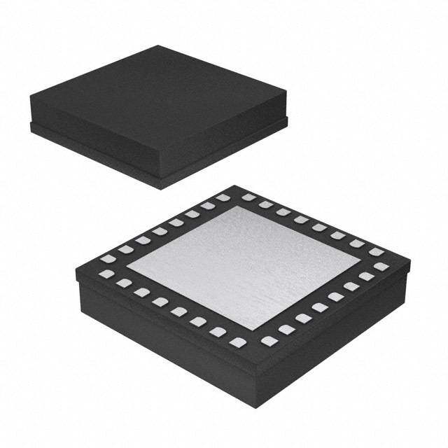
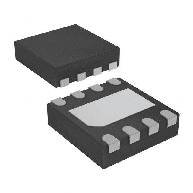
ICGOO电子元器件商城为您提供ADL5530ACPZ-R7由Analog设计生产,在icgoo商城现货销售,并且可以通过原厂、代理商等渠道进行代购。 ADL5530ACPZ-R7价格参考¥12.06-¥12.06。AnalogADL5530ACPZ-R7封装/规格:RF 放大器, 射频放大器 IC 手机,CDMA2000,W-CDMA,GSM 0Hz ~ 1GHz 8-LFCSP-VD(3x2)。您可以下载ADL5530ACPZ-R7参考资料、Datasheet数据手册功能说明书,资料中有ADL5530ACPZ-R7 详细功能的应用电路图电压和使用方法及教程。
ADL5530ACPZ-R7 是由 Analog Devices Inc.(ADI)生产的一款 RF(射频)放大器,属于 ADL5530 系列。该型号适用于多种射频和微波应用场合,以下是其主要应用场景的详细介绍:

1. 无线通信系统
   ADL5530ACPZ-R7 可广泛应用于无线通信基础设施,如基站、中继器和小型蜂窝设备。它能够提供高增益和线性性能,适合处理复杂的调制信号,例如 LTE、WCDMA 和其他现代无线通信标准中的信号。

2. 测试与测量设备
   在射频测试仪器中,这款放大器可用于信号源、频谱分析仪或网络分析仪等设备中,以提升信号强度并保持低失真特性,从而确保测量结果的准确性。

3. 雷达系统
   由于其宽带宽和高动态范围的特点,ADL5530ACPZ-R7 可用于雷达系统的发射链路中,帮助增强目标检测能力,并支持 X 波段及以下频率的应用。

4. 卫星通信
   在卫星地面站或用户终端中,该放大器可以用作上变频前级驱动放大器,为高频信号提供稳定的增益输出,同时减少噪声干扰。

5. 工业、科学和医疗 (ISM) 领域
   此类放大器也适用于 ISM 频段内的各种应用,例如无线传感器网络、远程监控设备以及医疗成像系统中的射频模块。

6. 航空航天与国防
   凭借其优异的电气特性和可靠性,ADL5530ACPZ-R7 能够满足航空航天和国防领域对高性能射频组件的需求,例如导航系统、电子对抗设备等。

总结来说,ADL5530ACPZ-R7 的应用场景集中在需要高性能射频信号处理的行业,包括但不限于通信、测试测量、雷达、卫星通信以及国防等领域。其关键优势在于高增益、宽带宽、低噪声以及良好的线性度,这些特性使其成为许多复杂射频系统的核心元件之一。
| 参数 | 数值 |
| 产品目录 | |
| 描述 | IC GAIN BLOCK IF 16.5DB 8-LFCSP |
| 产品分类 | |
| 品牌 | Analog Devices Inc |
| 数据手册 | |
| 产品图片 |
|
| P1dB | 21.4dBm(138mW) |
| 产品型号 | ADL5530ACPZ-R7 |
| RF类型 | 手机,CDMA2000,W-CDMA,GSM |
| rohs | 无铅 / 符合限制有害物质指令(RoHS)规范要求 |
| 产品系列 | - |
| 产品培训模块 | http://www.digikey.cn/PTM/IndividualPTM.page?site=cn&lang=zhs&ptm=24737 |
| 产品目录页面 | |
| 供应商器件封装 | 8-LFCSP-VD(3x2) |
| 其它名称 | ADL5530ACPZ-R7CT |
| 包装 | 剪切带 (CT) |
| 噪声系数 | 2.7dB ~ 3.5dB |
| 增益 | 13dB ~ 16dB |
| 封装/外壳 | 8-VFDFN 裸露焊盘,CSP |
| 标准包装 | 1 |
| 测试频率 | 900MHz |
| 电压-电源 | 3 V ~ 5 V |
| 电流-电源 | 110mA ~ 135mA |
| 视频文件 | http://www.digikey.cn/classic/video.aspx?PlayerID=1364138032001&width=640&height=505&videoID=2245193150001 |
| 频率 | 0Hz ~ 1GHz |


- 商务部:美国ITC正式对集成电路等产品启动337调查
- 曝三星4nm工艺存在良率问题 高通将骁龙8 Gen1或转产台积电
- 太阳诱电将投资9.5亿元在常州建新厂生产MLCC 预计2023年完工
- 英特尔发布欧洲新工厂建设计划 深化IDM 2.0 战略
- 台积电先进制程称霸业界 有大客户加持明年业绩稳了
- 达到5530亿美元!SIA预计今年全球半导体销售额将创下新高
- 英特尔拟将自动驾驶子公司Mobileye上市 估值或超500亿美元
- 三星加码芯片和SET,合并消费电子和移动部门,撤换高东真等 CEO
- 三星电子宣布重大人事变动 还合并消费电子和移动部门
- 海关总署:前11个月进口集成电路产品价值2.52万亿元 增长14.8%


PDF Datasheet 数据手册内容提取
DC to 1000 MHz IF Gain Block Data Sheet ADL5530 FEATURES FUNCTIONAL BLOCK DIAGRAM Fixed gain of 16.5 dB Operation up to 1000 MHz NC 1 8 GND 37 dBm Output Third-Order Intercept (OIP3) IN1 2 7 OUT1 3 dB noise figure NC 3 6 NC Input/output internally matched to 50 Ω S3t Va bolre 5 t eVm ppoewreart usurep apnlyd power supply NC 4NC=ANDOLC5O5N3N0ECT5 NC 05834-001 110 mA power supply current Figure 1. APPLICATIONS VCO buffers General purpose Tx/Rx amplification GENERAL DESCRIPTION The ADL5530 is a broadband, fixed-gain, linear amplifier that The ADL5530 operates with supply voltages of 3 V or 5 V with operates at frequencies up to 1000 MHz. The device can be used a supply current of 110 mA. in a wide variety of wired and wireless devices, including The ADL5530 is fabricated on a GaAs pHEMPT process. The cellular, broadband, CATV, and LMDS/MMDS applications. device is packaged in a 3 mm × 2 mm LFCSP that uses an The ADL5530 provides a gain of 16.5 dB, which is stable over exposed paddle for excellent thermal impedance. It operates frequency, temperature, power supply, and from device to from −40°C to +85°C. A fully populated evaluation board is device. It achieves an OIP3 of 37 dBm with an output also available. compression point of 21.8 dB and a noise figure of 3 dB. This amplifier is single-ended and internally matched to 50 Ω with an input return loss of 11 dB. Only input/output ac-coupling capacitors, a power supply decoupling capacitor, and an external inductor are required for operation. Rev. C Document Feedback Information furnished by Analog Devices is believed to be accurate and reliable. However, no responsibility is assumed by Analog Devices for its use, nor for any infringements of patents or other One Technology Way, P.O. Box 9106, Norwood, MA 02062-9106, U.S.A. rights of third parties that may result from its use. Specifications subject to change without notice. No license is granted by implication or otherwise under any patent or patent rights of Analog Devices. Tel: 781.329.4700 ©2006–2017 Analog Devices, Inc. All rights reserved. Trademarks and registered trademarks are the property of their respective owners. Technical Support www.analog.com
ADL5530 Data Sheet TABLE OF CONTENTS Features .............................................................................................. 1 Typical Performance Characteristics ..............................................7 Applications ....................................................................................... 1 Theory of Operation ...................................................................... 11 Functional Block Diagram .............................................................. 1 Soldering Information and Recommended PCB Land Pattern .......................................................................................... 11 General Description ......................................................................... 1 Evaluation Board ............................................................................ 12 Revision History ............................................................................... 2 Outline Dimensions ....................................................................... 14 Specifications ..................................................................................... 3 Ordering Guide .......................................................................... 14 Typical Scattering Parameters ..................................................... 4 Absolute Maximum Ratings ............................................................ 5 ESD Caution .................................................................................. 5 Pin Configuration and Function Descriptions ............................. 6 REVISION HISTORY 2/2017—Rev. B to Rev. C Changed CP-8-1 to CP-8-23 ........................................ Throughout Changes to Figure 2 ........................................................................... 6 Updated Outline Dimensions ........................................................ 14 Changes to Ordering Guide ........................................................... 14 7/2015—Rev. A to Rev. B Changes to Figure 26 ....................................................................... 13 Added Figure 27, Renumbered Sequentially ............................... 13 11/2013—Rev 0 to Rev. A Changes to Figure 2 ........................................................................... 6 Added Figure 15, Renumbered Sequentially ................................. 9 Added Exposed Pad Notation to Outline Dimensions .............. 13 Changes to Ordering Guide ........................................................... 13 7/2006—Revision 0: Initial Version Rev. C | Page 2 of 16
Data Sheet ADL5530 SPECIFICATIONS VPOS = 5 V and T = 25°C, unless otherwise noted. A Table 1. Parameter Conditions Min Typ Max Unit OVERALL FUNCTION (See Table 2) Frequency Range1 10 1000 MHz Gain (S21) 16.5 dB Input Return Loss (S11) −11 dB Output Return Loss (S22) −20 dB Reverse Isolation (S12) −21.5 dB FREQUENCY = 70 MHz Gain 15 16.7 18 dB vs. Temperature −40°C ≤ T ≤ +85°C ±0.1 dB A vs. Supply 4.75 V to 5.25 V ±0.02 dB Output 1 dB Compression Point 21.7 dBm Output Third-Order Intercept ∆f = 10 MHz , Output Power (P ) = 10 dBm per tone 37 dBm OUT Noise Figure 5 dB VPOS = 3 V 3.2 dB FREQUENCY = 190 MHz Gain 15 16.8 18.5 dB vs. Frequency ± 50 MHz ±0.1 dB vs. Temperature −40°C ≤ T ≤ +85°C ±0.2 dB A vs. Supply 4.75 V to 5.25 V ±0.02 dB Output 1 dB Compression Point 21.8 dBm Output Third-Order Intercept ∆f = 10 MHz , P = 10 dBm per tone 37 dBm OUT Noise Figure 3 4.5 dB VPOS = 3 V 2.3 dB FREQUENCY = 380 MHz Gain 14.8 16 17.3 dB vs. Frequency ± 50 MHz ±0.1 dB vs. Temperature −40°C ≤ T ≤ +85°C ±0.3 ±0.8 dB A vs. Supply 4.75 V to 5.25 V ±0.02 dB Output 1 dB Compression Point 19.5 21.6 dBm Output Third-Order Intercept ∆f = 10 MHz , P = 10 dBm per tone 36 dBm OUT Noise Figure 2.5 3.5 dB VPOS = 3 V 2 dB FREQUENCY = 900 MHz Gain 13 14.5 16 dB vs. Frequency ± 50 MHz ±0.2 dB vs. Temperature −40°C ≤ T ≤ +85°C ±0.5 ±1 dB A vs. Supply 4.75 V to 5.25 V ±0.02 dB Output 1 dB Compression Point 21.4 dBm Output Third-Order Intercept ∆f = 10 MHz , P = 10 dBm per tone 37 dBm OUT Noise Figure 2.7 3.5 dB VPOS = 3 V 2.3 dB POWER INTERFACE Pin VPOS Supply Voltage (VPOS) 3 5 5.5 V Supply Current 110 135 mA vs. Temperature −40°C ≤ T ≤ +85°C ±5 mA A Power Dissipation VPOS = 5 V 0.55 W VPOS = 3 V 0.33 W 1 For operation at lower frequencies, see the Theory of Operation section. Rev. C | Page 3 of 16
ADL5530 Data Sheet TYPICAL SCATTERING PARAMETERS VPOS = 5 V and T = 25°C. A Table 2. S11 S21 S12 S22 Freq. K (MHz) dB Magnitude Angle dB Magnitude Angle dB Magnitude Angle dB Magnitude Angle Factor 10 −7.1 0.44 −34 17.2 7.23 172 −22.5 0.08 22 −17.7 0.13 −69 0.94 20 −9.7 0.33 −26 16.7 6.81 174 −21.9 0.08 12 −24.4 0.06 −73 1.07 50 −11.2 0.28 −16 16.6 6.73 174 −21.7 0.08 4 −31.4 0.03 −42 1.10 100 −11.5 0.27 −13 16.5 6.70 171 −21.6 0.08 1 −30.4 0.03 −23 1.10 150 −11.4 0.27 −14 16.5 6.67 167 −21.6 0.08 −1 −29.3 0.03 −24 1.10 200 −11.5 0.27 −16 16.4 6.59 162 −21.6 0.08 −3 −27.7 0.04 −25 1.11 250 −11.4 0.27 −19 16.3 6.52 157 −21.6 0.08 −4 −26.6 0.05 −25 1.11 300 −11.4 0.27 −23 16.2 6.45 153 −21.6 0.08 −5 −25.1 0.06 −27 1.12 350 −11.3 0.27 −26 16.1 6.36 149 −21.6 0.08 −6 −23.7 0.07 −29 1.12 400 −11.2 0.27 −29 16.0 6.29 144 −21.6 0.08 −7 −22.2 0.08 −32 1.12 450 −11.1 0.28 −32 15.9 6.21 140 −21.6 0.08 −8 −20.7 0.09 −33 1.12 500 −11.1 0.28 −36 15.7 6.11 136 −21.6 0.08 −9 −19.6 0.10 −35 1.12 550 −11.0 0.28 −39 15.6 6.02 132 −21.7 0.08 −10 −18.4 0.12 −37 1.13 600 −10.9 0.29 −42 15.5 5.94 128 −21.7 0.08 −11 −17.3 0.14 −38 1.13 650 −10.8 0.29 −45 15.3 5.84 124 −21.6 0.08 −12 −16.4 0.15 −40 1.12 700 −10.7 0.29 −49 15.2 5.73 119 −21.6 0.08 −13 −15.5 0.17 −41 1.13 750 −10.6 0.29 −52 15.0 5.62 115 −21.6 0.08 −13 −14.6 0.19 −44 1.13 800 −10.6 0.30 −55 14.8 5.51 111 −21.6 0.08 −14 −13.8 0.20 −45 1.12 850 −10.4 0.30 −58 14.6 5.39 107 −21.6 0.08 −15 −13.1 0.22 −47 1.12 900 −10.3 0.30 −61 14.4 5.28 104 −21.6 0.08 −16 −12.4 0.24 −49 1.12 950 −10.2 0.31 −64 14.3 5.17 100 −21.6 0.08 −17 −11.7 0.26 −51 1.12 1000 −10.1 0.31 −66 14.1 5.06 96 −21.6 0.08 −18 −11.2 0.28 −52 1.11 Rev. C | Page 4 of 16
Data Sheet ADL5530 ABSOLUTE MAXIMUM RATINGS Table 3. Stresses at or above those listed under Absolute Maximum Parameter Rating Ratings may cause permanent damage to the product. This is a Supply Voltage, VPOS 6 V stress rating only; functional operation of the product at these Input Power (re: 50 Ω) 10 dBm or any other conditions above those indicated in the operational Internal Power Dissipation (Paddle Soldered) 600 mW section of this specification is not implied. Operation beyond θJC (Junction to Paddle) 154 °C/W the maximum operating conditions for extended periods may Maximum Junction Temperature 180 °C affect product reliability. Operating Temperature Range −40°C to +85°C ESD CAUTION Storage Temperature Range −65°C to +150°C Rev. C | Page 5 of 16
ADL5530 Data Sheet PIN CONFIGURATION AND FUNCTION DESCRIPTIONS NC 1 8 GND IN1 2 ADL5530 7 OUT1 TOP VIEW NC 3 (Not to Scale) 6 NC NC 4 5 NC NOTES 1.NC = NO CONNECT. 2.CITMHOPENE NEDEXACPNTOCESEDE G DTR OPO AGUDNNDDDL. EPS LOISAL NIDNEET.RE RTNOA AL LLYOW 05834-002 Figure 2. Pin Configuration Table 4. Pin Function Descriptions Pin No. Mnemonic Description 1, 3, 4, 5, 6 NC No Connect. 2 IN1 RF Input. Requires a DC blocking capacitor. 7 OUT1/ RF Output and VPOS (Supply Voltage). DC bias is provided to this pin through an inductor. RF path requires VPOS a DC blocking capacitor. 8 GND Ground. Connect this pin to a low impedance ground plane. Exposed Internally connected to GND. Solder to a low impedance ground plane. Paddle Rev. C | Page 6 of 16
Data Sheet ADL5530 TYPICAL PERFORMANCE CHARACTERISTICS 40 40 35 35 m) OIP3(10dBm) OIP3(5dBm) 3, NF (dB, dB 3205 P1dB NF (dB, dBm) 3205 GAIN, P1dB, OIP 211050 GAIN AIN, P1dB, OIP3, 211050 PG1AdINB G 05 NF 05834-003 05 NF 05834-006 0 100 200 300 400 500 600 700 800 900 1000 0 100 200 300 400 500 600 700 800 900 1000 FREQUENCY(MHz) FREQUENCY(MHz) Figure 3. Gain, P1dB, OIP3, and Noise Figure vs. Frequency, VPOS = 5 V Figure 6. Gain, P1dB, OIP3, and Noise Figure vs. Frequency, VPOS = 3 V 17.5 17.0 17.0 16.5 16.5 –40°C 5V 16.0 16.0 15.5 B) B)15.5 d15.0 d N ( +25°C N ( 3V AI14.5 AI G G15.0 14.0 +85°C 13.5 14.5 13.0 1122..05 05834-004 1134..50 05834-007 0 100 200 300 400 500 600 700 800 900 1000 0 100 200 300 400 500 600 700 800 900 1000 FREQUENCY(MHz) FREQUENCY(MHz) Figure 4. Gain vs. Frequency and Temperature, VPOS = 5 V Figure 7. Gain vs. Frequency and Supply, VPOS = 5 V and 3 V 25 18 0 20 GAIN 17 –5 15 16 –10 S11 B) P (dBm)OUT 1050 POUT 111543 GAIN (dB) S11, S22, S12 (d ––1250 S22 S12 –25 –5 12 –30 ––1150–30 –25 –20 IN–P15UTPO–W10ER(d–B5m) 0 5 101101 05834-005 –350 100 200 300 FR4E00QUE5N0C0Y(6M0H0z) 700 800 900 100005834-008 Figure 5. Output Power and Gain vs. Input Power, f = 190 MHz, VPOS = 5 V Figure 8. Input Return Loss, Output Return Loss, and Reverse Isolation vs. Frequency, VPOS = 5 V Rev. C | Page 7 of 16
ADL5530 Data Sheet 40 40 OIP3(–40°C) 38 39 38 36 34 OIP3(+85°C) 37 5V(10dBm) Bm) 32 OIP3(+25°C) 36 D P1dB (d 3208 P3 (dBm) 333543 OIP3 AN 2264 P1dB(+25°C) P1dB(–40°C) OI 3321 3V(5dBm) 22 30 20 P1dB(+85°C) 29 1168 05834-009 2278 05834-012 0 100 200 300 400 500 600 700 800 900 1000 0 100 200 300 400 500 600 700 800 900 1000 FREQUENCY(MHz) FREQUENCY(MHz) Figure 9. OIP3 and P1dB vs. Frequency and Temperature, VPOS = 5 V Figure 12. OIP3 vs. Frequency and Supply, VPOS = 5 V and 3 V 45 12 11 40 190MHz 10 900MHz 35 B) 9 d m) 380MHz E ( 8 dB 70MHz UR P3 ( 30 FIG 7 OI SE 6 25 OI N 5 4 5V 20 15 05834-010 23 3V 05834-013 0 2 4 6 8 10 12 14 16 18 20 22 24 0 100 200 300 400 500 600 700 800 900 1000 POUT(dBm) FREQUENCY(MHz) Figure 10. OIP3 vs. Output Power and Frequency, VPOS = 5 V Figure 13. Noise Figure vs. Frequency and Supply, VPOS = 5 V and 3 V 10 140 9 135 130 8 B) mA) 125 E (d 7 NT ( 120 5V R E U R OISE FIG 65 PLY CUR 111150 3V N P U 105 4 –40°C S +25°C 100 23 +85°C 05834-011 9905 05834-014 0 100 200 300 400 500 600 700 800 900 1000 –40 –30 –20 –10 0 10 20 30 40 50 60 70 80 90 FREQUENCY(MHz) TEMPERATURE(°C) Figure 11. Noise Figure vs. Frequency and Temperature, VPOS = 5 V Figure 14. Supply Current vs. Temperature and Supply, VPOS = 5 V and 3 V Rev. C | Page 8 of 16
Data Sheet ADL5530 150 5V, +25°C 6.0 5V, –40°C 140 5V, +85°C 3.3V, +25°C 5.5 3.3V, –40°C mA) 130 3.3V, +85°C 5.0 URRENT ( 111200 URE (dB) 4.5 BBRELLUADEC=K=+=8–54+°02C°5C°C C G 4.0 UPPLY 100 OISE FI 3.5 S 90 N 3.0 80 70–6 –4 –2 0 2 4 P6OUT 8(dB1m0) 12 14 16 18 20 22 05834-100 22..050 100 200 300 FR4E00QUE5N0C0Y(6M0H0z) 700 800 900 100005834-017 Figure 15. Supply Current vs. POUT and Temperature and Supply, Figure 18. Noise Figure Temperature Distribution, VPOS = 5 V VPOS = 5 V and 3 V 20 20 18 18 16 16 14 14 %) %) E ( 12 E ( 12 G G A A NT 10 NT 10 E E RC 8 RC 8 E E P P 6 6 4 4 02 05834-015 02 05834-018 30 31 32 33 34 35 36 37 38 39 40 41 42 43 44 45 15.5 15.9 16.3 16.7 17.1 17.5 17.9 18.3 15.7 16.1 16.5 16.9 17.3 17.7 18.1 18.5 OIP3(dBm) GAIN(dB) Figure 16. OIP3 Distribution at 190 MHz, 5 V Figure 19. Gain Distribution at 190 MHz, VPOS = 5 V 18 40 16 35 14 30 %) 12 %) E ( E ( 25 AG 10 AG NT NT 20 CE 8 CE ER ER 15 P 6 P 10 4 02 05834-016 05 05834-019 20.0 20.4 20.8 21.2 21.6 22.0 22.4 22.8 2.0 2.2 2.4 2.6 2.8 3.0 3.2 3.4 3.6 3.8 4.0 4.2 4.4 20.2 20.6 21.0 21.4 21.8 22.2 22.6 23.0 P1dB(dBm) NOISEFIGURE(dB) Figure 17. P1dB Distribution at 190 MHz, VPOS = 5 V Figure 20. Noise Figure Distribution at 190 MHz, VPOS = 5 V Rev. C | Page 9 of 16
ADL5530 Data Sheet 5.0 4.5 4.0 RE (dB) 3.5 BBRELLUADEC=K=+=8–54+°02C°5C°C U G 3.0 FI E OIS 2.5 N 2.0 11..50 05834-020 0 100 200 300 400 500 600 700 800 900 1000 FREQUENCY(MHz) Figure 21. Noise Figure Temperature Distribution, VPOS = 3 V Rev. C | Page 10 of 16
Data Sheet ADL5530 THEORY OF OPERATION The basic connections for operating the ADL5530 are shown in SOLDERING INFORMATION AND RECOMMENDED Figure 22. Recommended components are listed in Table 5. The PCB LAND PATTERN inputs and outputs should be ac coupled with appropriately Figure 24 shows the recommended land pattern for ADL5530. sized capacitors (device characterization was performed with To minimize thermal impedance, the exposed paddle on the 10 nF capacitors). DC bias is provided to the amplifier via an package underside should be soldered down to a ground plane inductor connected to the RF output pin. The bias voltage along with Pin 8. If multiple ground layers exist, they should be should be decoupled using a 10 nF capacitor. stitched together using vias. Pin 1, Pin 3, Pin 4, Pin 5 and Pin 6 can be left unconnected, or can be connected to ground. A bias voltage of 5 V is recommended. However, the device is Connecting these pins to ground slightly enhances thermal specified to operate down to 3 V with a slightly reduced impedance. compression point and a reduced noise figure. 3VTO5V PIN1 8 C5 10nF 0.46mm C1 1 NC GND 8 L4710nH 0.33mm 10nF RFIN 2 IN1 OUT1 7 RF OUT 0.53mm 0.5mm ADL5530 C2 10nF 3 NC NC 6 4 NC NC 5 05834-021 NC=NOCONNECT 00..3333mmmm 4 5 Figure 22. Basic Connections Freocro ompmereantidoend d (osween T taob 1le0 5M) aHlozn, ag lwaritghe rl abrigaesrin agc -cchooukpel iins g 2.13mm 05834-023 Figure 24. Recommended Land Pattern capacitors. Figure 23 shows a plot of input return loss and gain with the recommended components. Table 5. Recommended Components for Basic Connections Frequency C1 C2 L1 C5 10 MHz to 50 MHz 0.1 μF 0.1 μF 3.3 μH 0.1 μF 50 MHz to 1000 MHz 10 nF 10 nF 470 nH 10 nF 20 S21(3.3µH) 15 S21(470nH) 10 B) 1 (d 5 1 S D 0 N A N AI –5 S11(470nH) G –10 S11(3.3µH) ––2105 05834-022 5 10 15 20 25 30 35 40 45 50 FREQUENCY(MHz) Figure 23. Performance at 10 MHz Rev. C | Page 11 of 16
ADL5530 Data Sheet EVALUATION BOARD Figure 25 shows the schematic for the ADL5530 evaluation J5 VPOS board. The board is powered by a single supply (between 3 V C5 C6 C7 C10 and 5 V). 10nF OPEN OPEN OPEN J6 The components used on the board are listed in Table 6. Power GND can be applied to the board through clip-on leads (J5, J6), 1 NC GND 8 L1 C1 470nH through an edge connector (P1), or through Jumper W1. Note 10nF J1 2 IN1 OUT1 7 J2 that IN2, OUT2, T1, T2, C6, C7 and C10 have no function. IN1 ADL5530 C2 OUT1 10nF Because Pin 1, Pin 3 and Pin 6 of ADL5530 are No Connects, 3 NC NC 6 tehleecster ipcianl sp aerref ogrrmouanndcee)d. on this PCB (this has no effect on 4 NC NC 5 05834-024 NC=NOCONNECT Figure 25. Evaluation Board Schematic Rev. C | Page 12 of 16
Data Sheet ADL5530 05834-025 05834-027 Figure 26. Evaluation Board Layout, Top Layer Figure 27. Evaluation Board Layout, Bottom Layer Table 6. Evaluation Board Configuration Options Component Function Default Value C1, C2 AC-coupling capacitors. 10 nF 0402 C5 Power supply decoupling capacitor. 10 nF 0603 L1 DC bias inductor. 470 nH 1008 J5, J6 Clip-on terminals for power supply. J5 = VPOS J6 = GND W1 2-pin jumper for connection of ground and supply via cable. P1 Edge connector. P1: A1 to A5 = GND P1: B1 to B5 = GND P1: A8 to A9 = VPOS P1: B8 to B9 = VPOS Rev. C | Page 13 of 16
ADL5530 Data Sheet OUTLINE DIMENSIONS DETAIL A (JEDEC 95) 3.25 1.89 3.00 0.55 1.74 2.75 0.40 1.59 0.30 0.20 MIN 2.25 5 8 2.00 EXPOSED PAD 0.60 1.75 0.45 4 1 0.30 PIN 1 INDEX TOP VIEW BOTTOM VIEW PIN 1 AREA 0.50 BSC (INSEDEIC DAETTAOIRL AAR)EA OPTIONS 0.80 FOR PROPER CONNECTION OF 0.75 0.05 MAX THE EXPOSED PAD, REFER TO 0.70 0.02 NOM TFHUEN CPTINIO CNO DNEFSIGCURRIPATTIOIONNS AND SECTION OFTHIS DATA SHEET 0.30 PKG-004467 SEPALTAINNGE 00..2138 0.203 REF 02-13-2017-A Figure 28. 8-Lead Lead Frame Chip Scale Package [LFCSP] 2 mm × 3 mm Body and 0.75 mm Package Height (CP-8-23) Dimensions shown in millimeters ORDERING GUIDE Model1 Temperature Range Package Description Package Option Branding ADL5530ACPZ-R7 −40°C to +85°C 8-Lead LFCSP, 7” Tape and Reel CP-8-23 OT ADL5530ACPZ-WP −40°C to +85°C 8-Lead LFCSP, Waffle Pack CP-8-23 OT ADL5530-EVALZ Evaluation Board 1 Z = RoHS Compliant Part. Rev. C | Page 14 of 16
Data Sheet ADL5530 NOTES Rev. C | Page 15 of 16
ADL5530 Data Sheet NOTES ©2006–2017 Analog Devices, Inc. All rights reserved. Trademarks and registered trademarks are the property of their respective owners. D05834-0-2/17(C) Rev. C | Page 16 of 16