ICGOO在线商城 > 射频/IF 和 RFID > RF 放大器 > HMC478MP86E
 Datasheet下载
- 型号: HMC478MP86E
- 制造商: Hittite
- 库位|库存: xxxx|xxxx
- 要求:
| 数量阶梯 | 香港交货 | 国内含税 |
| +xxxx | $xxxx | ¥xxxx |
查看当月历史价格
查看今年历史价格
HMC478MP86E产品简介:
ICGOO电子元器件商城为您提供HMC478MP86E由Hittite设计生产,在icgoo商城现货销售,并且可以通过原厂、代理商等渠道进行代购。 HMC478MP86E价格参考。HittiteHMC478MP86E封装/规格:RF 放大器, RF Amplifier IC General Purpose 0Hz ~ 4GHz 。您可以下载HMC478MP86E参考资料、Datasheet数据手册功能说明书,资料中有HMC478MP86E 详细功能的应用电路图电压和使用方法及教程。
HMC478MP86E是Analog Devices Inc.推出的一款高性能射频(RF)放大器,属于宽频带、高增益的砷化镓(GaAs)MMIC放大器。该器件主要工作在20 MHz至6 GHz的宽频率范围内,适用于多种高频应用场景。

其典型应用包括:军用与民用通信系统,如软件定义无线电(SDR)、战术通信设备和宽带无线中继系统;电子战(EW)系统中的接收前端增益模块,用于增强微弱信号的灵敏度;测试与测量仪器,如频谱分析仪、信号发生器等,作为内部宽带放大单元提升系统性能;雷达系统中的本振(LO)驱动放大或接收链路低噪声放大后级增益级;以及卫星通信和地面微波链路中的射频信号放大。

HMC478MP86E具有高增益(典型值约21 dB)、良好的输入输出匹配特性及较高的线性度,支持直流偏置灵活调节,便于集成到复杂射频架构中。其采用8引脚陶瓷封装(MP86E),具备优良的散热与可靠性,适合严苛环境下的稳定运行。

综上,HMC478MP86E广泛应用于需要宽带、高线性度和高可靠性的国防、航空航天及高端通信系统中。
| 参数 | 数值 |
| 产品目录 | |
| 描述 | IC MMIC AMP HBT 4GHZ MICRO-P |
| 产品分类 | |
| 品牌 | Hittite Microwave Corporation |
| 数据手册 | |
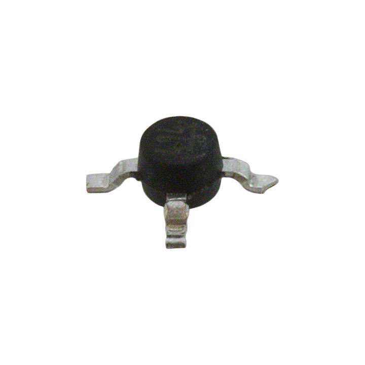
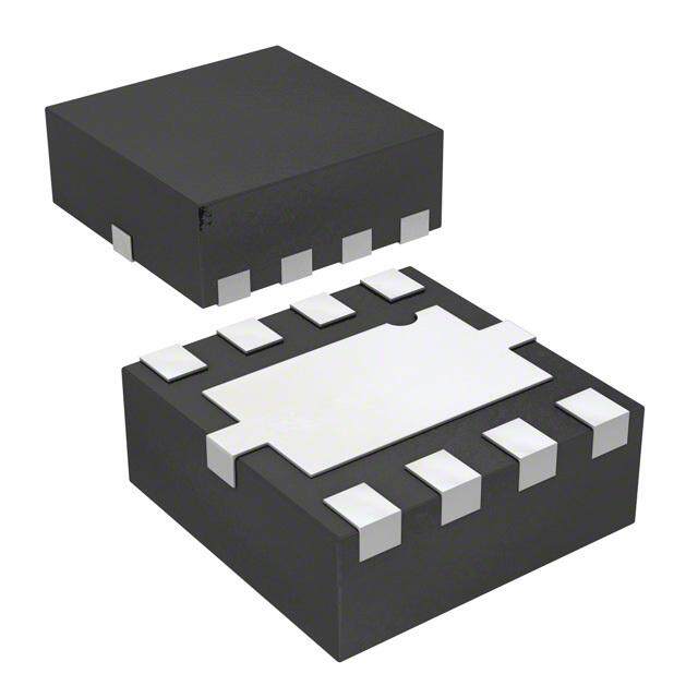
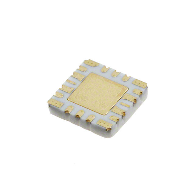
| 产品图片 |
|
| P1dB | 18dBm |
| 产品型号 | HMC478MP86E |
| RF类型 | 通用 |
| rohs | 无铅 / 符合限制有害物质指令(RoHS)规范要求 |
| 产品系列 | - |
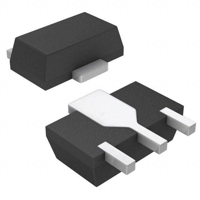
| 供应商器件封装 | SOT-86 |
| 其它名称 | 1127-1414 |
| 包装 | 散装 |
| 噪声系数 | 2.5dB ~ 3.5dB |
| 增益 | 22dB |
| 封装/外壳 | SOT-86 |
| 标准包装 | 100 |
| 测试频率 | - |
| 电压-电源 | 5 V ~ 8 V |
| 电流-电源 | 62mA |
| 频率 | 0Hz ~ 4GHz |


- 商务部:美国ITC正式对集成电路等产品启动337调查
- 曝三星4nm工艺存在良率问题 高通将骁龙8 Gen1或转产台积电
- 太阳诱电将投资9.5亿元在常州建新厂生产MLCC 预计2023年完工
- 英特尔发布欧洲新工厂建设计划 深化IDM 2.0 战略
- 台积电先进制程称霸业界 有大客户加持明年业绩稳了
- 达到5530亿美元!SIA预计今年全球半导体销售额将创下新高
- 英特尔拟将自动驾驶子公司Mobileye上市 估值或超500亿美元
- 三星加码芯片和SET,合并消费电子和移动部门,撤换高东真等 CEO
- 三星电子宣布重大人事变动 还合并消费电子和移动部门
- 海关总署:前11个月进口集成电路产品价值2.52万亿元 增长14.8%


PDF Datasheet 数据手册内容提取
HMC478MP86 478MP86E / v03.0810 SiGe HBT GAIN BLOCK MMIC AMPLIFIER, DC - 4 GHz Typical Applications Features 8 The HMC478MP86 / HMC478MP86E is an ideal RF/ P1dB Output Power: +18 dBm IF gain block & LO or PA driver: Gain: 22 dB • Cellular / PCS / 3G Output IP3: +32 dBm T • Fixed Wireless & WLAN Cascadable 50 Ohm I/Os M • CATV, Cable Modem & DBS Single Supply: +5V to +8V S • Microwave Radio & Test Equipment Robust 1,000V ESD, Class 1C - K Included in the HMC-DK001 Designer’s Kit C Functional Diagram General Description O L The HMC478MP86 & HMC478MP86E are SiGe B Heterojunction Bipolar Transistor (HBT) Gain Block MMIC SMT amplifi ers covering DC to 4 GHz. This N Micro-P packaged amplifi er can be used as a cas- I A cadable 50 Ohm RF/IF gain stage as well as a G LO or PA driver with up to +20 dBm output power. & The HMC478MP86(E) offers 22 dB of gain with a +32 dBm output IP3 at 850 MHz while requiring only R 62 mA from a single positive supply. The Darlington E V feedback pair used results in reduced sensitivity to I normal process variations and excellent gain stability R over temperature while requiring a minimal number of D external bias components. - S Electrical Specifi cations, Vs= 5V, Rbias= 18 Ohm, T = +25° C R A E Parameter Min. Typ. Max. Units I DC - 1.0 GHz 19 22 dB F 1.0 - 2.0 GHz 15 18 dB I Gain L 2.0 - 3.0 GHz 13 16 dB P 3.0 - 4.0 GHz 11 14 dB M Gain Variation Over Temperature DC - 4 GHz 0.015 0.02 dB/ °C A DC - 1.0 GHz 15 dB Input Return Loss 1.0 - 3.0 GHz 12 dB 3.0 - 4.0 GHz 13 dB DC - 1.0 GHz 20 dB Output Return Loss 1.0 - 4.0 GHz 17 dB Reverse Isolation DC - 4 GHz 20 dB 0.5 - 1.0 GHz 15 18 dBm 1.0 - 2.0 GHz 13 16 dBm Output Power for 1 dB Compression (P1dB) 2.0 - 3.0 GHz 11 14 dBm 3.0 - 4.0 GHz 9 12 dBm 0.5 - 2.0 GHz 32 dBm Output Third Order Intercept (IP3) 2.0 - 3.0 GHz 29 dBm (Pout= 0 dBm per tone, 1 MHz spacing) 3.0 - 4.0 GHz 25 dBm DC - 3.0 GHz 2.5 dB Noise Figure 3.0 - 4.0 GHz 3.5 dB Supply Current (Icq) 62 mA Note: Data taken with broadband bias tee on device output. InforFmaotiro np fruircniseh,e dd beyl iAvnealroyg Daenvidce st ois pbelaliecveed otor dbee arcsc:u rHateit taintde reMliaibcler. oHwowaevveer, Cnoo rpFoorr aptriiocen,, d2e0liv Aerlyp, haand R too apdla,c Ce horedlemrss: fAonrdal,o gM DAe v0ic1e8s2, 4Inc., responsibility is assumed by Analog Devices for its use, nor for any infringements of patents or other One Technology Way, P.O. Box 9106, Norwood, MA 02062-9106 8 - 1 rliicgehntss eo fi sth girrda nptaerdti ebsy t himatp mlicaaPyt iorhenso uonlrt ofertoh:m e9r wit7sis 8ues -eu2.n dS5epr0e ca-inf3iyc 3aptia4otne3sn ts ou rb jpeFacttae tnoxt c:r hig9ahn7tgs 8eo wf- 2Aithn5oau0lot g-n 3oDti3ecve7i.c 3eNso . POhrodnee:r 7 O81n-3-2li9n-e4 7a0t0 w(cid:127) Owrwde.hr oitntliitnee. cato wmww.analog.com Trademarks and registered trademarks arAe tphep plriocpearttyi oof nth eSir urespppecotivret :o wPnehrso.ne: 978-250-3A3p4p3li c aotrio na Spuppsp@orht: iPtthitoen.ec: o1-m800-ANALOG-D
HMC478MP86 / 478MP86E v03.0810 SiGe HBT GAIN BLOCK MMIC AMPLIFIER, DC - 4 GHz Broadband Gain & Return Loss Gain vs. Temperature 8 30 30 20 25 B) 10 20 NSE (d 0 SS2111 N (dB) 15 MT SPO S22 GAI S RE -10 10 - -20 5 ++2855 CC K -40 C C -30 0 O 0 1 2 3 4 5 6 7 8 0 1 2 3 4 5 FREQUENCY (GHz) FREQUENCY (GHz) L B N I Input Return Loss vs. Temperature Output Return Loss vs. Temperature A G 0 0 & -5 -5 B) B) R d -10 d -10 S ( S ( E S S O O V L -15 L -15 N N I R R R U U T -20 T -20 E +25 C E D R R +85 C -25 -40 C -25 ++2855 CC - -40 C S -30 -30 R 0 1 2 3 4 5 0 1 2 3 4 5 FREQUENCY (GHz) FREQUENCY (GHz) E I F I L P Reverse Isolation vs. Temperature Noise Figure vs. Temperature M 0 10 A 9 TION (dB) -1-05 ++-428055 CCC E (dB) 678 ++-428055 CCC A R L U O -15 G 5 E IS E FI 4 VERS -20 NOIS 3 RE -25 2 1 -30 0 0 1 2 3 4 5 0 1 2 3 4 5 FREQUENCY (GHz) FREQUENCY (GHz) InforFmaotiro np fruircniseh,e dd beyl iAvnealroyg Daenvidce st ois pbelaliecveed otor dbee arcsc:u rHateit taintde reMliaibcler. oHwowaevveer, Cnoo rpFoorr aptriiocen,, d2e0liv Aerlyp, haand R too apdla,c Ce horedlemrss: fAonrdal,o gM DAe v0ic1e8s2, 4Inc., responsibility is assumed by Analog Devices for its use, nor for any infringements of patents or other One Technology Way, P.O. Box 9106, Norwood, MA 02062-9106 rights of third parties that maPy rhesounlt fero:m 9 it7s 8us-e2. S5p0ec-if3ic3ati4on3s s u b jeFcta tox c: h9an7g8e w-2ith5ou0t -n3oti3ce7. 3No POhrodnee:r 7 O81n-3-2li9n-e4 7a0t0 w(cid:127) Owrwde.hr oitntliitnee. cato wmww.analog.com 8 - 2 license is granted by implication or otherwise under any patent or patent rights of Analog Devices. Trademarks and registered trademarks arAe tphep plriocpearttyi oof nth eSir urespppecotivret :o wPnehrso.ne: 978-250-3A3p4p3li c aotrio na Spuppsp@orht: iPtthitoen.ec: o1-m800-ANALOG-D
HMC478MP86 / 478MP86E v03.0810 SiGe HBT GAIN BLOCK MMIC AMPLIFIER, DC - 4 GHz P1dB vs. Temperature Psat vs. Temperature 8 24 24 22 22 20 20 18 18 16 16 SMT P1dB (dBm) 111024 Psat (dBm) 111024 - 68 ++2855 CC 68 ++2855CC K 4 -40 C 4 -40C C 2 2 0 0 O 0 1 2 3 4 5 0 1 2 3 4 5 L FREQUENCY (GHz) FREQUENCY (GHz) B N Gain, Power & OIP3 vs. Supply Voltage I A Output IP3 vs. Temperature for Constant Icc= 62 mA @ 850 MHz G 35 m) 36 & 30 P3 (dB 32 R OI 28 E m) 25 Bm), 24 RIV OIP3 (dB 20 m), Psat (d 1260 S - D 15 ++-428055 CCC B), P1dB (dB 1482 GPPO1saIdPainBt3 R 100 1 2 3 4 5 ain (d 05 6 7 8 G E FREQUENCY (GHz) Vs (Vdc) I F I L Vcc vs. Icc Over Temperature for Gain, Power & OIP3 vs. Supply Voltage P Fixed Vs= 5V, RBIAS= 18 Ohms for Rs = 18 Ohms @ 850 MHz M 80 m) 36 A dB 75 +85 C 3 ( 32 P 6750 +25 C dBm), OI 2248 Icc (mA) 5650 m), Psat ( 1260 -40 C dB 12 50 dB ( 8 PG1adinB P1 Psat 45 B), 4 OIP3 d 40 n ( 0 3.7 3.8 3.9 4 4.1 4.2 4.3 Gai 4.5 5 5.5 Vcc (Vdc) Vs (Vdc) InforFmaotiro np fruircniseh,e dd beyl iAvnealroyg Daenvidce st ois pbelaliecveed otor dbee arcsc:u rHateit taintde reMliaibcler. oHwowaevveer, Cnoo rpFoorr aptriiocen,, d2e0liv Aerlyp, haand R too apdla,c Ce horedlemrss: fAonrdal,o gM DAe v0ic1e8s2, 4Inc., responsibility is assumed by Analog Devices for its use, nor for any infringements of patents or other One Technology Way, P.O. Box 9106, Norwood, MA 02062-9106 8 - 3 rliicgehntss eo fi sth girrda nptaerdti ebsy t himatp mlicaaPyt iorhenso uonlrt ofertoh:m e9r wit7sis 8ues -eu2.n dS5epr0e ca-inf3iyc 3aptia4otne3sn ts ou rb jpeFacttae tnoxt c:r hig9ahn7tgs 8eo wf- 2Aithn5oau0lot g-n 3oDti3ecve7i.c 3eNso . POhrodnee:r 7 O81n-3-2li9n-e4 7a0t0 w(cid:127) Owrwde.hr oitntliitnee. cato wmww.analog.com Trademarks and registered trademarks arAe tphep plriocpearttyi oof nth eSir urespppecotivret :o wPnehrso.ne: 978-250-3A3p4p3li c aotrio na Spuppsp@orht: iPtthitoen.ec: o1-m800-ANALOG-D
HMC478MP86 / 478MP86E v03.0810 SiGe HBT GAIN BLOCK MMIC AMPLIFIER, DC - 4 GHz Absolute Maximum Ratings 8 Collector Bias Voltage (Vcc) +6.0 Vdc ELECTROSTATIC SENSITIVE DEVICE Collector Bias Current (Icc) 100 mA OBSERVE HANDLING PRECAUTIONS RF Input Power (RFIN)(Vcc = +4.3 Vdc) +5 dBm Junction Temperature 150 °C T Continuous Pdiss (T = 85 °C) M 0.583 W (derate 9 mW/°C above 85 °C) S Thermal Resistance 111.5 °C/W (junction to lead) - Storage Temperature -65 to +150 °C K C Operating Temperature -40 to +85 °C O ESD Sensitivity (HBM) Class 1C L B Outline Drawing N I A G & R E V I R D - S R E NOTES: I 1. LEADFRAME MATERIAL: COPPER ALLOY F 2. DIMENSIONS ARE IN INCHES [MILLIMETERS] I L 3. DIMENSION DOES NOT INCLUDE MOLDFLASH OF 0.15mm PER SIDE. P 4. ALL GROUND LEADS MUST BE SOLDERED TO PCB RF GROUND. M 5. THE MICRO-P PACKAGE IS DIMENSIONALLY COMPATIBLE WITH THE “MICRO-X PACKAGE” A Package Information Part Number Package Body Material Lead Finish MSL Rating Package Marking HMC478MP86 Low Stress Injection Molded Plastic Sn/Pb Solder MSL1 [1] 478 HMC478MP86E RoHS-compliant Low Stress Injection Molded Plastic 100% matte Sn MSL1 [2] 478 [1] Max peak refl ow temperature of 235 °C [2] Max peak refl ow temperature of 260 °C InforFmaotiro np fruircniseh,e dd beyl iAvnealroyg Daenvidce st ois pbelaliecveed otor dbee arcsc:u rHateit taintde reMliaibcler. oHwowaevveer, Cnoo rpFoorr aptriiocen,, d2e0liv Aerlyp, haand R too apdla,c Ce horedlemrss: fAonrdal,o gM DAe v0ic1e8s2, 4Inc., responsibility is assumed by Analog Devices for its use, nor for any infringements of patents or other One Technology Way, P.O. Box 9106, Norwood, MA 02062-9106 rights of third parties that maPy rhesounlt fero:m 9 it7s 8us-e2. S5p0ec-if3ic3ati4on3s s u b jeFcta tox c: h9an7g8e w-2ith5ou0t -n3oti3ce7. 3No POhrodnee:r 7 O81n-3-2li9n-e4 7a0t0 w(cid:127) Owrwde.hr oitntliitnee. cato wmww.analog.com 8 - 4 license is granted by implication or otherwise under any patent or patent rights of Analog Devices. Trademarks and registered trademarks arAe tphep plriocpearttyi oof nth eSir urespppecotivret :o wPnehrso.ne: 978-250-3A3p4p3li c aotrio na Spuppsp@orht: iPtthitoen.ec: o1-m800-ANALOG-D
HMC478MP86 / 478MP86E v03.0810 SiGe HBT GAIN BLOCK MMIC AMPLIFIER, DC - 4 GHz Pin Descriptions 8 Pin Number Function Description Interface Schematic This pin is DC coupled. 1 RFIN An off chip DC blocking capacitor is required. T M S 3 RFOUT RF output and DC Bias (Vcc) for the output stage. - K C 2, 4 GND These pins must be connected to RF/DC ground. O L B N Application Circuit I A G & R E V I R D - S R E I F I L P M A Recommended Bias Resistor Values for Icc= 62 mA, Rbias= (Vs - Vcc) / Icc Supply Voltage (Vs) 5V 6V 8V Note: 1. External blocking capacitors are required on RBIAS VALUE 18 Ω 35 Ω 67 Ω RFIN and RFOUT. RBIAS POWER RATING 1/8 W 1/4 W 1/2 W 2. RBIAS provides DC bias stability over temperature. Recommended Component Values for Key Application Frequencies Frequency (MHz) Component 50 900 1900 2200 2400 3500 L1 270 nH 56 nH 18 nH 18 nH 15 nH 8.2 nH C1, C2 0.01 μF 100 pF 100 pF 100 pF 100 pF 100 pF InforFmaotiro np fruircniseh,e dd beyl iAvnealroyg Daenvidce st ois pbelaliecveed otor dbee arcsc:u rHateit taintde reMliaibcler. oHwowaevveer, Cnoo rpFoorr aptriiocen,, d2e0liv Aerlyp, haand R too apdla,c Ce horedlemrss: fAonrdal,o gM DAe v0ic1e8s2, 4Inc., responsibility is assumed by Analog Devices for its use, nor for any infringements of patents or other One Technology Way, P.O. Box 9106, Norwood, MA 02062-9106 8 - 5 rliicgehntss eo fi sth girrda nptaerdti ebsy t himatp mlicaaPyt iorhenso uonlrt ofertoh:m e9r wit7sis 8ues -eu2.n dS5epr0e ca-inf3iyc 3aptia4otne3sn ts ou rb jpeFacttae tnoxt c:r hig9ahn7tgs 8eo wf- 2Aithn5oau0lot g-n 3oDti3ecve7i.c 3eNso . POhrodnee:r 7 O81n-3-2li9n-e4 7a0t0 w(cid:127) Owrwde.hr oitntliitnee. cato wmww.analog.com Trademarks and registered trademarks arAe tphep plriocpearttyi oof nth eSir urespppecotivret :o wPnehrso.ne: 978-250-3A3p4p3li c aotrio na Spuppsp@orht: iPtthitoen.ec: o1-m800-ANALOG-D
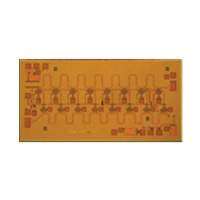
HMC478MP86 / 478MP86E v03.0810 SiGe HBT GAIN BLOCK MMIC AMPLIFIER, DC - 4 GHz Evaluation PCB 8 T M S - K C O L B N I A G & R E V I R D - S R E I F I L List of Materials for Evaluation PCB 110170 [1] P M The circuit board used in the application should use Item Description A RF circuit design techniques. Signal lines should J1 - J2 PCB Mount SMA Connector have 50 Ohm impedance while the package ground J3 - J4 DC Pin leads should be connected directly to the ground C1, C2 Capacitor, 0402 Pkg. plane similar to that shown. A sufficient number C3 100 pF Capacitor, 0402 Pkg. of via holes should be used to connect the top C4 1000 pF Capacitor, 0603 Pkg. and bottom ground planes. The evaluation board C5 2.2 μF Capacitor, Tantalum should be mounted to an appropriate heat sink. R1 Resistor, 1210 Pkg. The evaluation circuit board shown is available from L1 Inductor, 0603 Pkg. Hittite upon request. U1 HMC478MP86 / HMC478MP86E PCB [2] 107087 Evaluation PCB [1] Reference this number when ordering complete evaluation PCB [2] Circuit Board Material: Rogers 4350 InforFmaotiro np fruircniseh,e dd beyl iAvnealroyg Daenvidce st ois pbelaliecveed otor dbee arcsc:u rHateit taintde reMliaibcler. oHwowaevveer, Cnoo rpFoorr aptriiocen,, d2e0liv Aerlyp, haand R too apdla,c Ce horedlemrss: fAonrdal,o gM DAe v0ic1e8s2, 4Inc., responsibility is assumed by Analog Devices for its use, nor for any infringements of patents or other One Technology Way, P.O. Box 9106, Norwood, MA 02062-9106 rights of third parties that maPy rhesounlt fero:m 9 it7s 8us-e2. S5p0ec-if3ic3ati4on3s s u b jeFcta tox c: h9an7g8e w-2ith5ou0t -n3oti3ce7. 3No POhrodnee:r 7 O81n-3-2li9n-e4 7a0t0 w(cid:127) Owrwde.hr oitntliitnee. cato wmww.analog.com 8 - 6 license is granted by implication or otherwise under any patent or patent rights of Analog Devices. Trademarks and registered trademarks arAe tphep plriocpearttyi oof nth eSir urespppecotivret :o wPnehrso.ne: 978-250-3A3p4p3li c aotrio na Spuppsp@orht: iPtthitoen.ec: o1-m800-ANALOG-D