ICGOO在线商城 > 射频/IF 和 RFID > RF 放大器 > THS9001DBVT

 Datasheet下载
- 型号: THS9001DBVT
- 制造商: Texas Instruments
- 库位|库存: xxxx|xxxx
- 要求:
| 数量阶梯 | 香港交货 | 国内含税 |
| +xxxx | $xxxx | ¥xxxx |
查看当月历史价格
查看今年历史价格
THS9001DBVT产品简介:
ICGOO电子元器件商城为您提供THS9001DBVT由Texas Instruments设计生产,在icgoo商城现货销售,并且可以通过原厂、代理商等渠道进行代购。 THS9001DBVT价格参考¥4.78-¥9.70。Texas InstrumentsTHS9001DBVT封装/规格:RF 放大器, 射频放大器 IC 手机,CDMA,TDMA,PCS 50MHz ~ 350MHz SOT-23-6。您可以下载THS9001DBVT参考资料、Datasheet数据手册功能说明书,资料中有THS9001DBVT 详细功能的应用电路图电压和使用方法及教程。
Texas Instruments(德州仪器)的THS9001DBVT是一款RF(射频)放大器,广泛应用于高频信号处理领域。以下是其主要应用场景:

1. 无线通信设备:
   THS9001DBVT适用于无线通信系统中的信号放大,例如蜂窝基站、Wi-Fi路由器和物联网(IoT)设备。它能够高效处理高频射频信号,确保数据传输的稳定性和可靠性。

2. 雷达系统:
   在雷达应用中,该放大器可用于信号增强,提高目标检测的灵敏度和精度。其低噪声特性和高增益性能使其成为理想选择。

3. 卫星通信:
   用于卫星地面站或卫星终端设备中,对上行和下行链路信号进行放大,以减少信号损耗并提升通信质量。

4. 测试与测量设备:
   在高性能示波器、频谱分析仪和其他测试设备中,THS9001DBVT可作为信号驱动放大器,提供精确的信号输出和输入处理能力。

5. 医疗设备:
   在超声波成像等医疗应用中,这款放大器可用于增强接收信号,从而提高图像分辨率和诊断准确性。

6. 工业自动化:
   在工业无线传感器网络(WSN)中,THS9001DBVT可用于放大传感器节点的射频信号,支持远程监控和数据采集。

7. 广播系统:
   用于广播电视发射机或中继站,确保音频和视频信号的高质量传输。

总之,THS9001DBVT凭借其出色的射频性能(如宽带宽、低失真和高线性度),在需要高效处理高频信号的各种电子系统中发挥重要作用。
| 参数 | 数值 |
| 产品目录 | |
| 描述 | IC 350MHZ CASCADABLE AMP SOT23-6射频放大器 50-MHz to 350-MHz Cascadeable Amp |
| DevelopmentKit | THS9001EVM |
| 产品分类 | |
| 品牌 | Texas Instruments |
| 产品手册 | http://www.ti.com/litv/slos426c |
| 产品图片 |
|
| rohs | 符合RoHS无铅 / 符合限制有害物质指令(RoHS)规范要求 |
| 产品系列 | RF集成电路,射频放大器,Texas Instruments THS9001DBVT- |
| 数据手册 | |
| P1dB | 20.6 dBm |
| 产品型号 | THS9001DBVT |
| RF类型 | 手机,CDMA,TDMA,PCS |
| 产品培训模块 | http://www.digikey.cn/PTM/IndividualPTM.page?site=cn&lang=zhs&ptm=26085 |
| 产品目录页面 | |
| 产品种类 | 射频放大器 |
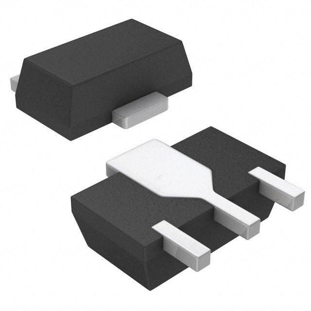
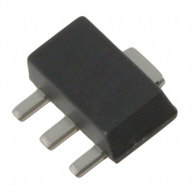
| 供应商器件封装 | SOT-23-6 |
| 其它名称 | 296-16645-6 |
| 制造商产品页 | http://www.ti.com/general/docs/suppproductinfo.tsp?distId=10&orderablePartNumber=THS9001DBVT |
| 功率增益类型 | 15 dB |
| 包装 | Digi-Reel® |
| 单位重量 | 10 mg |
| 商标 | Texas Instruments |
| 噪声系数 | 4 dB |
| 增益 | 15dB |
| 安装风格 | SMD/SMT |
| 封装 | Reel |
| 封装/外壳 | SOT-23-6 |
| 封装/箱体 | SOT-23-6 |
| 工作电源电压 | 2.7 V to 5.5 V |
| 工作频率 | 50 MHz to 350 MHz |
| 工厂包装数量 | 250 |
| 最大功率耗散 | 463 mW |
| 最大工作温度 | + 85 C |
| 最小工作温度 | - 40 C |
| 标准包装 | 1 |
| 测试频率 | 350 MHz |
| 电压-电源 | 5V |
| 电流-电源 | 100mA |
| 电源电流 | 100 mA |
| 类型 | Cascadable Amplifier |
| 系列 | THS9001 |
| 输出截获点 | 37 dBm |
| 通道数量 | 1 Channel |
| 配用 | /product-detail/zh/THS9001EVM/296-18860-ND/863693/product-detail/zh/THS9000EVM/296-18859-ND/863692 |
| 频率 | 50MHz ~ 350MHz |


- 商务部:美国ITC正式对集成电路等产品启动337调查
- 曝三星4nm工艺存在良率问题 高通将骁龙8 Gen1或转产台积电
- 太阳诱电将投资9.5亿元在常州建新厂生产MLCC 预计2023年完工
- 英特尔发布欧洲新工厂建设计划 深化IDM 2.0 战略
- 台积电先进制程称霸业界 有大客户加持明年业绩稳了
- 达到5530亿美元!SIA预计今年全球半导体销售额将创下新高
- 英特尔拟将自动驾驶子公司Mobileye上市 估值或超500亿美元
- 三星加码芯片和SET,合并消费电子和移动部门,撤换高东真等 CEO
- 三星电子宣布重大人事变动 还合并消费电子和移动部门
- 海关总署:前11个月进口集成电路产品价值2.52万亿元 增长14.8%


PDF Datasheet 数据手册内容提取
THS9001 www.ti.com SLOS426C–NOVEMBER2003–REVISEDDECEMBER2013 50 MHz to 750 MHz CASCADEABLE AMPLIFIER CheckforSamples:THS9001 FEATURES APPLICATIONS 1 • HighDynamicRange • IFAmplifiers 2 – OIP =36dBm – TDMA:GSM,IS-136,EDGE/UWE-136 3 – NF< 4.5dB – CDMA:IS-95,UMTS,CDMA2000 • Single-SupplyVoltage – WirelessLocalLoops • HighSpeed – WirelessLAN:IEEE802.11 – V =3Vto5V S – I =Adjustable S • Input/OutputImpedance – 50Ω DESCRIPTION The THS9001 is a medium power, cascadeable, gain block optimized for high IF frequencies. The amplifier incorporates internal impedance matching to 50 Ω, and achieves greater than 15-dB input, and output return loss from 50 MHz to 350 MHz with V = 5 V, R = 237 Ω, L = 470 nH. Design requires only 2 dc-blocking S (BIAS) (COL) capacitors,1power-supplybypasscapacitor,1RFchoke,and1biasresistor. FunctionBlockDiagram V S THS9001 R (BIAS) IF (IN) 1 6 C IN IF (OUT) 2 5 C OUT 3 4 L (COL) C (BYP) V S 1 Pleasebeawarethatanimportantnoticeconcerningavailability,standardwarranty,anduseincriticalapplicationsof TexasInstrumentssemiconductorproductsanddisclaimerstheretoappearsattheendofthisdatasheet. Alltrademarksarethepropertyoftheirrespectiveowners. 2 PRODUCTIONDATAinformationiscurrentasofpublicationdate. Copyright©2003–2013,TexasInstrumentsIncorporated Products conform to specifications per the terms of the Texas Instruments standard warranty. Production processing does not necessarilyincludetestingofallparameters.
THS9001 SLOS426C–NOVEMBER2003–REVISEDDECEMBER2013 www.ti.com Thesedeviceshavelimitedbuilt-inESDprotection.Theleadsshouldbeshortedtogetherorthedeviceplacedinconductivefoam duringstorageorhandlingtopreventelectrostaticdamagetotheMOSgates. AVAILABLEOPTIONS PACKAGEDDEVICE(1) PACKAGETYPE TRANSPORTMEDIA,QUANTITY THS9001DBVT TapeandReel,250 SOT-23-6 THS9001DBVR TapeandReel,3000 (1) Forthemostcurrentpackageandorderinginformation,seethePackageOptionAddendumattheend ofthisdocument,orseetheTIWebsiteatwww.ti.com. ABSOLUTE MAXIMUM RATINGS Overoperatingfree-airtemperature(unlessotherwisenoted)(1) UNIT V Supplyvoltage,GNDtoV 5.5 SS S V Inputvoltage GNDtoV I S Continuouspowerdissipation SeeDissipationRating table T Maximumjunctiontemperature 150°C J T Maximumjunctiontemperature,continuousoperation,longtermreliability (2) 125°C J T Storagetemperature –65to150°C stg ESDRatings HBM 2000 : CDM 1500 MM 100 (1) Theabsolutemaximumratingsunderanyconditionislimitedbytheconstraintsofthesiliconprocess.Stressesabovetheseratingsmay causepermanentdamage.Exposuretoabsolutemaximumconditionsforextendedperiodsmaydegradedevicereliability.Theseare stressratingsonly,andfunctionaloperationofthedeviceattheseoranyotherconditionsbeyondthosespecifiedisnotimplied. (2) Themaximumjunctiontemperatureforcontinuousoperationislimitedbypackageconstraints.Operationabovethistemperaturemay resultinreducedreliabilityand/orlifetimeofthedevice. DISSIPATION RATING TABLE θ θ POWERRATING(1) PACKAGE JC JA (°C/W) (°C/W) T ≤25°C T =85°C A A DBV(2) 70.1 215 463W 185mW (1) Powerratingisdeterminedwithajunctiontemperatureof125°C.ThermalmanagementofthefinalPCBshouldstrivetokeepthe junctiontemperatureatorbelow125°Cforbestperformance. (2) ThisdatawastakenusingtheJEDECstandardHigh-KtestPCB. RECOMMENDED OPERATING CONDITIONS MIN NOM MAX UNIT V Supplyvoltage 2.7 5 V SS T Operatingfree-airtemperature, –40 85 °C A I Supplycurrent 100 mA S 2 SubmitDocumentationFeedback Copyright©2003–2013,TexasInstrumentsIncorporated ProductFolderLinks:THS9001
THS9001 www.ti.com SLOS426C–NOVEMBER2003–REVISEDDECEMBER2013 ELECTRICAL CHARACTERISTICS TypicalPerformance(V =5V,R =237Ω,L =470nH)(unlessotherwisenoted) S (BIAS) (COL) PARAMETER TESTCONDITIONS MIN TYP MAX UNITS f=50MHz 15.8 Gain dB f=350MHz 15 f=50MHz 35 OIP dBm 3 f=350MHz 37 f=50MHz 20.6 1-dBcompression dBm f=350MHz 20.6 f=50MHz 15.4 Inputreturnloss dB f=350MHz 16.6 f=50MHz 17 Outputreturnloss dB f=350MHz 15 f=50MHz 20.7 Reverseisolation dB f=350MHz 20.7 f=50MHz 3.7 Noisefigure dB f=350MHz 4 PINASSIGNMENT 1 6 IF BIAS (IN) 2 5 GND IF (OUT) 3 4 VS L(COL) TerminalFunctions PINNUMBERS NAME DESCRIPTION 1 IF Signalinput (IN) 2 GND Negativepower-supplyinput 3 V Positivepower-supplyinput S 4 L Outputtransistorloadinductor (COL) 5 IF Signaloutput (OUT) 6 BIAS Biascurrentinput SIMPLIFIEDSCHEMATIC VS L(COL) BIAS IF(IN) IF(OUT) GND Copyright©2003–2013,TexasInstrumentsIncorporated SubmitDocumentationFeedback 3 ProductFolderLinks:THS9001
THS9001 SLOS426C–NOVEMBER2003–REVISEDDECEMBER2013 www.ti.com TABLE OF GRAPHS FIGURE S21Frequencyresponse 1 S22Frequencyresponse 2 S11Frequencyresponse 3 S12Frequencyresponse 4 S21 vsR 5 (Bias) Noisefigure vsFrequency 6 I Supplycurrent vsR 7 S (Bias) OutputpowervsInputpower 8 Adjacentchannel(ACPR)andAlternatechannel vsInputpower 9 (AltCPR)protectionratios OIP vsFrequency 10 2 OIP vsFrequency 11 3 S21Frequencyresponse 12 S22Frequencyresponse 13 S11Frequencyresponse 14 S12Frequencyresponse vsFrequency 15 Noisefigure 16 OIP vsFrequency 17 2 Outputpower vsInputpower 18 OIP vsFrequency 19 3 4 SubmitDocumentationFeedback Copyright©2003–2013,TexasInstrumentsIncorporated ProductFolderLinks:THS9001
THS9001 www.ti.com SLOS426C–NOVEMBER2003–REVISEDDECEMBER2013 TYPICAL CHARACTERISTICS S-ParametersofTHS9000asmountedontheEVMwithV =5V,R =237Ω,andL =68nHto470nHatroom S (BIAS) (COL) temperature. S21FREQUENCYRESPONSE S22FREQUENCYRESPONSE 17 0 L(COL)=100nH VS=5V, L(COL)=470nH L(COL)=220nH R(BIAS)=237W 16 L(COL)=330nH L(COL)=68nH −5 15 B d B − 14 d 21 2− −10 S 2 S 13 L(COL)=100nH L(COL)=220nH 12 L(COL)=68nH −15 L(COL)=330nH 11 VS=5V, L(COL)=470nH R(BIAS)=237W −20 10 1M 10M 100M 1G 1M 10M 100M 1G f−Frequency−Hz f−Frequency−Hz Figure1. Figure2. S11FREQUENCYRESPONSE S12FREQUENCYRESPONSE 0 −15 −5 L(COL)=68nH VRS(B=IA5S)V=,237W L(COL)=470nH −20 −10 L(COL)=100nH L(COL)=330nH −15 L(COL)=220nH B −25 d B − d 11 −20 L(COL)=330nH − S 12 L(COL)=220nH S −30 −25 L(COL)=470nH L(COL)=100nH −30 −35 L(COL)=68nH −35 VS=5V, R(BIAS)=237W −40 −40 1M 10M 100M 1G 1M 10M 100M 1G f−Frequency−Hz f−Frequency−Hz Figure3. Figure4. Copyright©2003–2013,TexasInstrumentsIncorporated SubmitDocumentationFeedback 5 ProductFolderLinks:THS9001
THS9001 SLOS426C–NOVEMBER2003–REVISEDDECEMBER2013 www.ti.com TYPICAl CHARACTERISTICS S-ParametersofTHS9000asmountedontheEVMwithV =3Vand5V,R =various,andL =470nHatroom S (BIAS) (COL) temp. S21 NOISEFIGURE vs vs R FREQUENCY (BIAS) 17 5 R(BIAS)=56.2W,VS=3V 16 4.75 VS=5V,IS=99mA 4.5 VS=5V,IS=75mA 15 R(BIAS)=237W, VS=5V B 21−dB 1134 RR(B(BIAIASS))==9374.70WW,V,VSS==35VV Figure−d 4.245 VS=5V,VISS==530Vm,IAS=94mA S R(BIAS)=549W,VS=5V oise 3.75 VS=3V,IS=49mA N 12 VS=3V,IS=70mA R(BIAS)=174W,VS=3V 3.5 11 VS=3V to5V, 3.25 L(col)=470nH 10 3 1M 10M 100M 1G 50 150 250 350 450 500 f−Frequency−Hz f−Frequency−MHz Figure5. Figure6. SUPPLYCURRENT OUTPUTPOWER vs vs R INPUTPOWER (BIAS) 200 22 VS=5V,IS=99mA 21 180 20 VS=5V,IS=75mA 160 m 19 A B −m 140 −d 18 VS=5V,IS=50mA rent 120 ower 17 Cur VS=5V utP 16 y 100 p ppl Out 15 VS=3V,IS=94mA u −S 80 −O 14 VS=3V,IS=70mA IS 60 VS=3V P 13 12 40 VS=3V,IS=49mA 11 f=100MHz 20 10 50 150 250 350 450 550 −6 −4 −2 0 2 4 6 8 10 12 14 R(BIAS)− W PI−InputPower−dBm Figure7. Figure8. 6 SubmitDocumentationFeedback Copyright©2003–2013,TexasInstrumentsIncorporated ProductFolderLinks:THS9001
THS9001 www.ti.com SLOS426C–NOVEMBER2003–REVISEDDECEMBER2013 TYPICAl CHARACTERISTICS (continued) S-ParametersofTHS9000asmountedontheEVMwithV =3Vand5V,R =various,andL =470nHatroom S (BIAS) (COL) temp. ADJACENTCHANNEL(ACPR)andALTERNATE CHANNEL(AltCPR)PROTECTIONRATIOS vs OIP 2 INPUTPOWER vs WCDMModulation,f=1.8432MHz,PAR=10.4dB FREQUENCY -20 50 VS= 5 V L(COL)=470nH -30 ILS = 9=9 2m2A0 nH ACPR 48 ISV=S9=43mVA, ISV=S9=95mVA, (col) 46 AltCPR -40 B d m 44 − B o d ati -50 − 42 R 2 ower OIP 40 IVSS==755Vm,A ISV=S7=03mVA, P -60 SourceACPR 38 -70 SourceAltCPR 36 ISV=S4=93mVA, VISS==550Vm,A -80 34 -21 -18 -15 -12 -9 -6 -3 0 3 0 50 100 150 200 250 300 Input Power−dBM f−Frequency−MHz Figure9. Figure10. OIP 3 vs FREQUENCY 40 L(COL)=470nH 38 VS=5V,IS=99mA 36 VS=5V,IS=75mA m 34 dB VS=3V,IS=94mA −3 32 VS=3V,IS=70mA P OI VS=5V,IS=50mA 30 28 VS=3V,IS=49mA 26 24 0 100 200 300 400 500 f−Frequency−MHz Figure11. Copyright©2003–2013,TexasInstrumentsIncorporated SubmitDocumentationFeedback 7 ProductFolderLinks:THS9001
THS9001 SLOS426C–NOVEMBER2003–REVISEDDECEMBER2013 www.ti.com TYPICAL CHARACTERISTICS THS9000asmountedontheEVMwithV =3Vand5V,R =237Ω,andL =470nHat–40°C,25°C,and85°C. S (BIAS) (COL) S21FREQUENCYRESPONSE S22FREQUENCYRESPONSE 17 0 −45oC −2 VS=5V, R(BIAS)=237W, 16 −4 L(COL)=470nH 25oC 15 −6 85oC −8 B 14 d B − d −10 S21 13 22− −12 85oC S 12 −14 25oC −16 11 VRS(B=IA5S)V=,237W, −18 −45oC L(col)=470nH 10 −20 1M 10M 100M 1G 1M 10M 100M 1G f−Frequency−Hz f−Frequency−Hz Figure12. Figure13. S11FREQUENCYRESPONSE S12FREQUENCYRESPONSE 0 −15 −5 VRS(B=IA5S)V=,237W, VRS(B=IA5S)V=,237W, L(COL)=470nH L(COL)=470nH −20 −10 −15 −45oC B 25oC d −25 − −20 85oC dB 11 − 85oC S 2 −25 S1 −30 −30 −35 −45oC −35 −40 25oC −45 −40 1M 10M 100M 1G 1M 10M 100M 1G f−Frequency−MHz f−Frequency−Hz Figure14. Figure15. 8 SubmitDocumentationFeedback Copyright©2003–2013,TexasInstrumentsIncorporated ProductFolderLinks:THS9001
THS9001 www.ti.com SLOS426C–NOVEMBER2003–REVISEDDECEMBER2013 TYPICAL CHARACTERISTICS (continued) THS9000asmountedontheEVMwithV =3Vand5V,R =237Ω,andL =470nHat–40°C,25°C,and85°C. S (BIAS) (COL) NOISEFIGURE OIP 3 vs vs FREQUENCY FREQUENCY 6 48 5.5 VRL(S(CBO=IAL5S))=V=,427307nWH, 85oC 47 VRL(S(CBO=IAL5S))=V=,427307nWH, −45oC 46 B 5 −d Bm 45 25oC e d gur 4.5 25oC −2 44 85oC Fi P e OI ois 43 N 4 42 3.5 −45oC 41 40 3 0 100 200 300 400 500 50 100 150 200 250 300 f−Frequency−MHz f−Frequency−MHz Figure16. Figure17. OUTPUTPOWER OIP 3 vs vs INPUTPOWER FREQUENCY 22 40 21 VRLf=(S(CB1O=IA0L5S0))=VM=,4H273z07nWH, 25oC 39 VRL(S(CBO=IAL5S))=V=,427307nWH, 85oC Bm 20 −45oC 38 d 25oC − er 19 m 37 w B o d P − put 18 85oC P3 36 Out 17 OI 35 −45oC − O P 16 34 15 33 14 32 −2 0 2 4 6 8 10 12 50 100 150 200 250 300 350 400 450 500 PI−InputPower−dBm f−Frequency−MHz Figure18. Figure19. Copyright©2003–2013,TexasInstrumentsIncorporated SubmitDocumentationFeedback 9 ProductFolderLinks:THS9001
THS9001 SLOS426C–NOVEMBER2003–REVISEDDECEMBER2013 www.ti.com TYPICAL CHARACTERISTICS Table1.S-ParametersTablesofTHS9001withEVMDe-Embedded V =5V,R =237,L =470nH S (BIAS) (COL) S21 S11 S22 S12 Frequency Gain(dB) Phase(deg) Gain(dB) Phase(deg) Gain(dB) Phase(deg) Gain(dB) Phase(deg) (MHz) 1.0 -3.5 -165.0 -2.3 -1.1 -2.6 174.8 -64.4 -121.7 5.0 11.7 -127.1 -1.5 -14.9 -2.8 140.4 -32.4 123.0 10.2 15.8 -150.1 -2.2 -42.3 -5.3 99.8 -23.6 79.5 19.7 16.3 -170.8 -6.6 -69.3 -10.7 64.5 -21.1 40.7 50.1 15.9 175.7 -16.2 -90.3 -16.2 33.9 -20.6 14.5 69.7 15.8 171.5 -21.1 -95.4 -16.9 26.4 -20.6 9.4 102.4 15.7 165.7 -32.3 -86.5 -17.1 19.9 -20.6 5.3 150.5 15.6 158.2 -28.0 45.9 -16.8 14.7 -20.7 2.1 198.1 15.5 151.1 -21.9 46.8 -16.2 10.8 -20.7 0.1 246.9 15.3 144.1 -18.9 37.2 -15.3 6.0 -20.7 -1.4 307.6 15.2 135.3 -16.0 27.8 -14.2 -1.8 -20.6 -3.9 362.8 15.0 127.8 -14.2 17.4 -13.3 -9.2 -20.6 -5.9 405.0 14.9 121.9 -12.8 10.9 -12.6 -16.0 -20.6 -8.2 452.2 14.7 115.4 -11.6 3.0 -11.8 -23.9 -20.6 -10.8 504.7 14.5 108.4 -10.3 -6.0 -10.9 -33.0 -20.7 -14.2 563.4 14.4 100.3 -8.9 -17.4 -9.8 -45.2 -20.9 -19.3 595.3 14.2 96.0 -8.2 -23.3 -9.2 -52.2 -21.0 -22.6 664.5 14.1 87.0 -6.7 -36.9 -8.0 -68.3 -21.7 -30.5 702.1 14.0 80.9 -5.9 -44.6 -7.3 -79.1 -22.5 -38.6 741.8 13.9 76.5 -5.1 -54.0 -6.8 -91.4 -24.0 -44.9 828.1 13.5 62.2 -4.3 -76.1 -6.3 -113.2 -26.5 -35.0 874.9 13.0 54.0 -4.1 -84.6 -5.9 -126.0 -27.0 -49.0 924.4 12.8 44.9 -3.6 -93.1 -5.1 -136.8 -28.0 -62.9 976.7 11.6 35.9 -3.5 -104.4 -5.3 -157.8 -34.0 -104.4 1031.9 11.1 33.0 -3.4 -115.7 -5.8 -172.3 -37.1 107.9 1090.3 10.4 29.2 -3.3 -122.0 -5.7 -173.4 -37.8 162.5 1151.9 10.3 22.2 -3.0 -131.3 -4.8 179.4 -31.1 169.5 1217.1 9.7 4.7 -2.9 -142.3 -3.9 161.9 -26.3 137.1 1285.9 8.6 0.7 -2.9 -151.7 -3.6 147.6 -22.7 121.9 1358.6 7.3 -8.3 -2.9 -161.2 -3.4 134.6 -20.6 116.5 1435.5 5.8 -14.5 -3.0 -170.1 -3.2 122.6 -18.8 105.2 1516.6 4.6 -22.7 -3.1 -178.6 -3.2 112.1 -17.2 96.0 1602.4 3.2 -28.4 -3.1 173.2 -3.1 101.7 -15.7 87.0 1693.0 1.5 -38.0 -3.1 165.1 -3.0 92.4 -14.3 79.2 1788.8 -0.5 -47.9 -3.1 157.6 -2.9 83.6 -13.1 68.8 1889.9 -2.5 -51.0 -3.2 148.8 -2.7 74.4 -12.4 56.9 1996.8 -4.1 -49.0 -3.4 139.5 -2.3 65.0 -12.2 48.2 10 SubmitDocumentationFeedback Copyright©2003–2013,TexasInstrumentsIncorporated ProductFolderLinks:THS9001
THS9001 www.ti.com SLOS426C–NOVEMBER2003–REVISEDDECEMBER2013 APPLICATION INFORMATION The THS9001 is a medium power, cascadeable, amplifier optimized for high intermediate frequencies in radios. The amplifier is unconditionally stable and the design requires only 2 dc-blocking capacitors, 1 power-supply bypasscapacitor,1RFchoke,and1biasresistor.RefertoFigure25 forthecircuitdiagram. TheTHS901operateswithapower-supplyvoltagerangingfrom2.5Vto5.5V. The value of R sets the bias current to the amplifier. Refer to Figure 14. This allows the designer to trade-off (BIAS) linearityversuspowerconsumption.R canberemovedwithoutdamagetothedevice. (BIAS) Component selection of C , C , and C is not critical. The values shown in Figure 25 were used for all the (BYP) IN OUT datashowninthisdatasheet. The amplifier incorporates internal impedance matching to 50 Ω that can be adjusted for various frequencies of operationbyproperselectionofL . (COL) Figure 20 shows the s-parameters of the part mounted on the standard EVM with V = 5 V, R = 237 Ω, and S (BIAS) L = 470 nH. With this configuration, the part is very broadband, and achieves greater than 15-dB input and (COL) outputreturnlossfrom50MHzto325MHz. 17 0 S11 VS=5V, R(BIAS)=237W 16 S22 L(COL)=470nH −5 S21 15 −10 B d B 14 − d 2 − −15 S2 S21 13 ,12 S S12 −20 11, S 12 −25 11 −30 1 M 10 M 100 M 1 G f - Frequency - Hz Figure20.S-ParametersofTHS9001MountedontheStandardEVMwithV =5V,R =237Ω, S (BIAS) andL =470nH (COL) Copyright©2003–2013,TexasInstrumentsIncorporated SubmitDocumentationFeedback 11 ProductFolderLinks:THS9001
THS9001 SLOS426C–NOVEMBER2003–REVISEDDECEMBER2013 www.ti.com Figure21showsanexampleofasingleconversionreceiverarchitectureandwheretheTHS9001wouldtypically beused. 900 MHz−2 GHz 900 MHz−2 GHz Image Rejection IFAmp 1 IFAmp 2 Filter LNA1 LNA2 Mixer IF SAW PGA IF SAW ADC LO Drive LO Drive RX LO Amp 1 Amp 2 THS9001 2x for Diversity Figure21. ExampleSingleConversionReceiverArchitecture Figure 22 shows an example of a dual conversion receiver architecture and where the THS9001 would typically beused. 900 MHz−2 GHz 100 MHz−300 MHz 20 MHz−70 MHz Image Reject 1st IFAmp 2nd IFAmp1 LNA1 LNA2 Filter 1st Mixer 1st IF SAW PGA 2nd Mixer 2nd IF SAW2AnmdpI2F Alias Filter ADC LO1 Drive LO1 Drive RX LO 1 Amp 1 Amp 2 RX LO2 LOA2m Dpr 1iveLOA2m Dpr 2ive THS9001 2x for Diversity Figure22. ExampleDualConversionReceiverArchitecture Figure 23 shows an example of a dual conversion transmitter architecture and where the THS9001 would typicallybeused. BB 100 MHz−300 MHz 900 MHz−2 GHz 1st IF amp DAC BBAmp Alias Filter 1st Mixer IF SAW PGA 2nd Mixer PA LO2 Drive LO2 Drive RX LO1 LO1 Drive LO1 Drive RX LO2 Amp 1 Amp 2 Amp 1 Amp 2 THS9001 2x for Diversity Figure23. ExampleDualConversionTransmitterArchitecture 12 SubmitDocumentationFeedback Copyright©2003–2013,TexasInstrumentsIncorporated ProductFolderLinks:THS9001
THS9001 www.ti.com SLOS426C–NOVEMBER2003–REVISEDDECEMBER2013 Figure 24 shows the THS9001 and Sawtek #854916 SAW filter frequency response along with the frequency responseoftheSAWfilteralone.TheSAWfilterhasacenterfrequencyof140MHzwith10-MHzbandwidthand 8-dB insertion loss. It can be seen that the frequency response with the THS9001 is the same as with the SAW except for a 15-dB gain. The THS9001 is mounted on the standard EVM with V = 5 V, R = 237 Ω, and S (BIAS) L =470nH.Notetheamplifierdoesnotaddartifactstothesignal. (COL) SAW+THS90001 SAW THS9001 RED= SAW 140 MHz SAWOnly Green = 140 MHZ SAW: Sawtek #854916 Figure24. FrequencyResponseoftheTHS9000andSAWFilter,andSAWFilterOnly V S THS9001 R (BIAS) IF (IN) 1 6 C IN COUT IF(OUT) 2 5 1 nF 3 4 L (COL) C (BYP) 0.1mF VS Figure25. THS9000RecommendedCircuit(usedforalltests) Copyright©2003–2013,TexasInstrumentsIncorporated SubmitDocumentationFeedback 13 ProductFolderLinks:THS9001
THS9001 SLOS426C–NOVEMBER2003–REVISEDDECEMBER2013 www.ti.com Evaluation Module BillOfMaterialsisthebillofmaterials,andFigure26 andFigure27showtheEVMlayout. BillOfMaterials ITEM DESCRIPTION REFDES QTY PARTNUMBER(1) 1 Cap,0.1μF,ceramic,X7R,50V C1 1 (AVX)08055C104KAT2A 2 Cap,1000pF,ceramic,NPO,100V C2,C3 2 (AVX)08051A102JAT2A 3 Inductor,470nH,5% L1 1 (Coilcraft)0805CS-471XJBC 4 Resistor,237Ω,1/8W,1% R1 1 (Phycomp)9C08052A2370FKHFT 5 Open TR1 1 6 Jack,bananareceptance,0.25"dia. J3,J4 2 (SPC)813 7 Connector,edge,SMAPCBjack J1,J2 2 (Johnson)142-0701-801 8 Standoff,4-40Hex,0.625"Length 4 (KEYSTONE)1808 9 Screw,Phillips,4-40,.250" 4 SHR-0440-016-SN 10 IC,THS90001 U1 1 (TI)THS9001DBV 11 Board,printed-circuit 1 (TI)EDGE#6453522Rev.A (1) Themanufacturer'spartnumbersareusedfortestpurposesonly. Figure26. EVMTopLayout Figure27. EVMBottomLayout 14 SubmitDocumentationFeedback Copyright©2003–2013,TexasInstrumentsIncorporated ProductFolderLinks:THS9001
THS9001 www.ti.com SLOS426C–NOVEMBER2003–REVISEDDECEMBER2013 0.085 0.053 Pin1 0.008 0.040 0.032 0.032 TOPVIEW Figure28. THS9000RecommendedFootprintdimensionsareininches(millimeters) Copyright©2003–2013,TexasInstrumentsIncorporated SubmitDocumentationFeedback 15 ProductFolderLinks:THS9001
THS9001 SLOS426C–NOVEMBER2003–REVISEDDECEMBER2013 www.ti.com REVISION HISTORY ChangesfromRevisionB(January2007)toRevisionC Page • ChangedthedatasheettitleFrom:50MHzto400MHzCASCADEABLEAMPLIFIERTo:50MHzto750MHz CASCADEABLEAMPLIFIER ............................................................................................................................................... 1 16 SubmitDocumentationFeedback Copyright©2003–2013,TexasInstrumentsIncorporated ProductFolderLinks:THS9001
PACKAGE OPTION ADDENDUM www.ti.com 6-Feb-2020 PACKAGING INFORMATION Orderable Device Status Package Type Package Pins Package Eco Plan Lead/Ball Finish MSL Peak Temp Op Temp (°C) Device Marking Samples (1) Drawing Qty (2) (6) (3) (4/5) THS9001DBVT ACTIVE SOT-23 DBV 6 250 Green (RoHS NIPDAU Level-1-260C-UNLIM -40 to 85 NWL & no Sb/Br) (1) The marketing status values are defined as follows: ACTIVE: Product device recommended for new designs. LIFEBUY: TI has announced that the device will be discontinued, and a lifetime-buy period is in effect. NRND: Not recommended for new designs. Device is in production to support existing customers, but TI does not recommend using this part in a new design. PREVIEW: Device has been announced but is not in production. Samples may or may not be available. OBSOLETE: TI has discontinued the production of the device. (2) RoHS: TI defines "RoHS" to mean semiconductor products that are compliant with the current EU RoHS requirements for all 10 RoHS substances, including the requirement that RoHS substance do not exceed 0.1% by weight in homogeneous materials. Where designed to be soldered at high temperatures, "RoHS" products are suitable for use in specified lead-free processes. TI may reference these types of products as "Pb-Free". RoHS Exempt: TI defines "RoHS Exempt" to mean products that contain lead but are compliant with EU RoHS pursuant to a specific EU RoHS exemption. Green: TI defines "Green" to mean the content of Chlorine (Cl) and Bromine (Br) based flame retardants meet JS709B low halogen requirements of <=1000ppm threshold. Antimony trioxide based flame retardants must also meet the <=1000ppm threshold requirement. (3) MSL, Peak Temp. - The Moisture Sensitivity Level rating according to the JEDEC industry standard classifications, and peak solder temperature. (4) There may be additional marking, which relates to the logo, the lot trace code information, or the environmental category on the device. (5) Multiple Device Markings will be inside parentheses. Only one Device Marking contained in parentheses and separated by a "~" will appear on a device. If a line is indented then it is a continuation of the previous line and the two combined represent the entire Device Marking for that device. (6) Lead/Ball Finish - Orderable Devices may have multiple material finish options. Finish options are separated by a vertical ruled line. Lead/Ball Finish values may wrap to two lines if the finish value exceeds the maximum column width. Important Information and Disclaimer:The information provided on this page represents TI's knowledge and belief as of the date that it is provided. TI bases its knowledge and belief on information provided by third parties, and makes no representation or warranty as to the accuracy of such information. Efforts are underway to better integrate information from third parties. TI has taken and continues to take reasonable steps to provide representative and accurate information but may not have conducted destructive testing or chemical analysis on incoming materials and chemicals. TI and TI suppliers consider certain information to be proprietary, and thus CAS numbers and other limited information may not be available for release. In no event shall TI's liability arising out of such information exceed the total purchase price of the TI part(s) at issue in this document sold by TI to Customer on an annual basis. Addendum-Page 1
PACKAGE MATERIALS INFORMATION www.ti.com 22-Nov-2013 TAPE AND REEL INFORMATION *Alldimensionsarenominal Device Package Package Pins SPQ Reel Reel A0 B0 K0 P1 W Pin1 Type Drawing Diameter Width (mm) (mm) (mm) (mm) (mm) Quadrant (mm) W1(mm) THS9001DBVT SOT-23 DBV 6 250 180.0 9.0 3.15 3.2 1.4 4.0 8.0 Q3 PackMaterials-Page1
PACKAGE MATERIALS INFORMATION www.ti.com 22-Nov-2013 *Alldimensionsarenominal Device PackageType PackageDrawing Pins SPQ Length(mm) Width(mm) Height(mm) THS9001DBVT SOT-23 DBV 6 250 182.0 182.0 20.0 PackMaterials-Page2
PACKAGE OUTLINE DBV0006A SOT-23 - 1.45 mm max height SCALE 4.000 SMALL OUTLINE TRANSISTOR C 3.0 2.6 0.1 C 1.75 1.45 B A 1.45 MAX PIN 1 INDEX AREA 1 6 2X 0.95 3.05 2.75 1.9 5 2 4 3 0.50 6X 0.25 0.15 0.2 C A B (1.1) TYP 0.00 0.25 GAGE PLANE 0.22 TYP 0.08 8 TYP 0.6 0 0.3 TYP SEATING PLANE 4214840/B 03/2018 NOTES: 1. All linear dimensions are in millimeters. Any dimensions in parenthesis are for reference only. Dimensioning and tolerancing per ASME Y14.5M. 2. This drawing is subject to change without notice. 3. Body dimensions do not include mold flash or protrusion. Mold flash and protrusion shall not exceed 0.15 per side. 4. Leads 1,2,3 may be wider than leads 4,5,6 for package orientation. 5. Refernce JEDEC MO-178. www.ti.com
EXAMPLE BOARD LAYOUT DBV0006A SOT-23 - 1.45 mm max height SMALL OUTLINE TRANSISTOR PKG 6X (1.1) 1 6X (0.6) 6 SYMM 2 5 2X (0.95) 3 4 (R0.05) TYP (2.6) LAND PATTERN EXAMPLE EXPOSED METAL SHOWN SCALE:15X SOLDER MASK SOLDER MASK METAL UNDER METAL OPENING OPENING SOLDER MASK EXPOSED METAL EXPOSED METAL 0.07 MAX 0.07 MIN ARROUND ARROUND NON SOLDER MASK SOLDER MASK DEFINED DEFINED (PREFERRED) SOLDER MASK DETAILS 4214840/B 03/2018 NOTES: (continued) 6. Publication IPC-7351 may have alternate designs. 7. Solder mask tolerances between and around signal pads can vary based on board fabrication site. www.ti.com
EXAMPLE STENCIL DESIGN DBV0006A SOT-23 - 1.45 mm max height SMALL OUTLINE TRANSISTOR PKG 6X (1.1) 1 6X (0.6) 6 SYMM 2 5 2X(0.95) 3 4 (R0.05) TYP (2.6) SOLDER PASTE EXAMPLE BASED ON 0.125 mm THICK STENCIL SCALE:15X 4214840/B 03/2018 NOTES: (continued) 8. Laser cutting apertures with trapezoidal walls and rounded corners may offer better paste release. IPC-7525 may have alternate design recommendations. 9. Board assembly site may have different recommendations for stencil design. www.ti.com
IMPORTANTNOTICEANDDISCLAIMER TI PROVIDES TECHNICAL AND RELIABILITY DATA (INCLUDING DATASHEETS), DESIGN RESOURCES (INCLUDING REFERENCE DESIGNS), APPLICATION OR OTHER DESIGN ADVICE, WEB TOOLS, SAFETY INFORMATION, AND OTHER RESOURCES “AS IS” AND WITH ALL FAULTS, AND DISCLAIMS ALL WARRANTIES, EXPRESS AND IMPLIED, INCLUDING WITHOUT LIMITATION ANY IMPLIED WARRANTIES OF MERCHANTABILITY, FITNESS FOR A PARTICULAR PURPOSE OR NON-INFRINGEMENT OF THIRD PARTY INTELLECTUAL PROPERTY RIGHTS. These resources are intended for skilled developers designing with TI products. You are solely responsible for (1) selecting the appropriate TI products for your application, (2) designing, validating and testing your application, and (3) ensuring your application meets applicable standards, and any other safety, security, or other requirements. These resources are subject to change without notice. TI grants you permission to use these resources only for development of an application that uses the TI products described in the resource. Other reproduction and display of these resources is prohibited. No license is granted to any other TI intellectual property right or to any third party intellectual property right. TI disclaims responsibility for, and you will fully indemnify TI and its representatives against, any claims, damages, costs, losses, and liabilities arising out of your use of these resources. TI’s products are provided subject to TI’s Terms of Sale (www.ti.com/legal/termsofsale.html) or other applicable terms available either on ti.com or provided in conjunction with such TI products. TI’s provision of these resources does not expand or otherwise alter TI’s applicable warranties or warranty disclaimers for TI products. Mailing Address: Texas Instruments, Post Office Box 655303, Dallas, Texas 75265 Copyright © 2020, Texas Instruments Incorporated