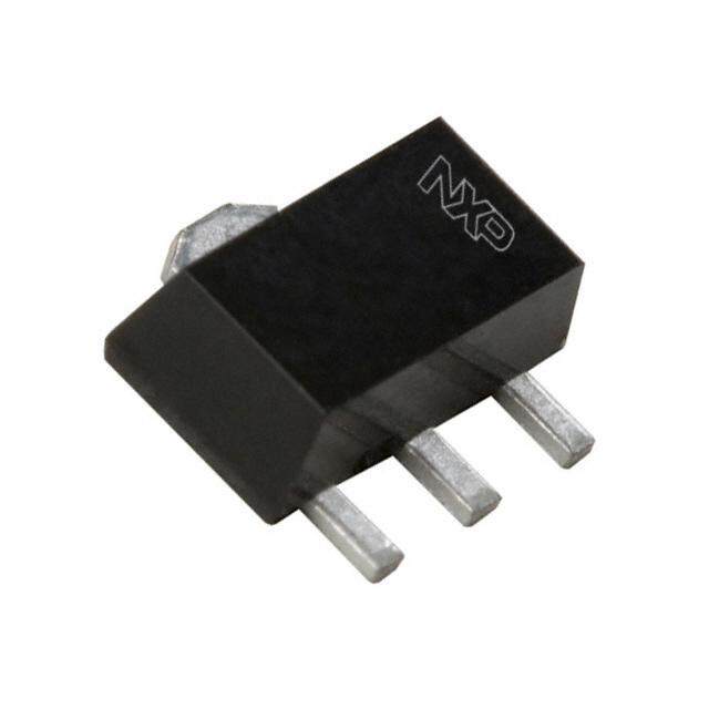
ICGOO在线商城 > 射频/IF 和 RFID > RF 放大器 > SKY65111-348LF

 Datasheet下载
- 型号: SKY65111-348LF
- 制造商: SKYWORKS
- 库位|库存: xxxx|xxxx
- 要求:
| 数量阶梯 | 香港交货 | 国内含税 |
| +xxxx | $xxxx | ¥xxxx |
查看当月历史价格
查看今年历史价格
SKY65111-348LF产品简介:
ICGOO电子元器件商城为您提供SKY65111-348LF由SKYWORKS设计生产,在icgoo商城现货销售,并且可以通过原厂、代理商等渠道进行代购。 SKY65111-348LF价格参考。SKYWORKSSKY65111-348LF封装/规格:RF 放大器, RF Amplifier IC ISM 600MHz ~ 1.1GHz 16-QFN (3x3)。您可以下载SKY65111-348LF参考资料、Datasheet数据手册功能说明书,资料中有SKY65111-348LF 详细功能的应用电路图电压和使用方法及教程。
SKY65111-348LF 是由 Skyworks Solutions Inc. 生产的一款射频(RF)放大器,属于高性能、低功耗的前端模块,主要应用于无线通信系统中。该器件典型工作频率范围覆盖 2.4 GHz 至 2.5 GHz ISM 频段,适用于需要高线性度和高效能的短距离无线传输场景。

其主要应用场景包括:
1. 无线局域网(WLAN):广泛用于 Wi-Fi 4(802.11n)、Wi-Fi 5(802.11ac)等标准的 2.4 GHz 频段设备中,如家庭路由器、接入点和无线网卡。
2. 物联网(IoT)设备:适用于智能家居产品(如智能灯泡、传感器、安防设备)中的无线连接模块,提供稳定可靠的射频信号放大功能。
3. 工业无线通信:用于工业自动化系统中的无线数据传输,支持远程监控与控制,具备良好的抗干扰能力。
4. 消费类电子产品:集成于智能手机周边配件、无线耳机、可穿戴设备等,提升无线信号发射功率和通信距离。

SKY65111-348LF 采用紧凑型封装,具有高增益、低噪声和优异的输出功率特性,能够在低电压下实现高效运行,适合对空间和功耗敏感的应用。同时,其内置匹配电路简化了设计流程,有助于加快产品开发周期。总体而言,该 RF 放大器是现代无线连接解决方案中的关键组件之一。
| 参数 | 数值 |
| 产品目录 | |
| 描述 | IC AMP INGAP 600-110MHZ 12-QFN射频放大器 600-1100MHz 2W InGaP HBT 3 Stage |
| 产品分类 | |
| 品牌 | Skyworks Solutions, Inc. |
| 产品手册 | |
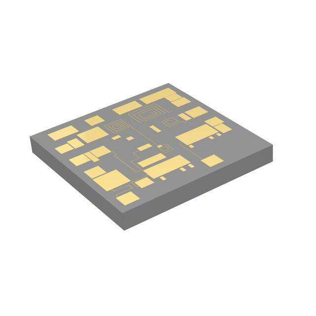
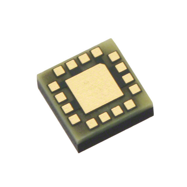
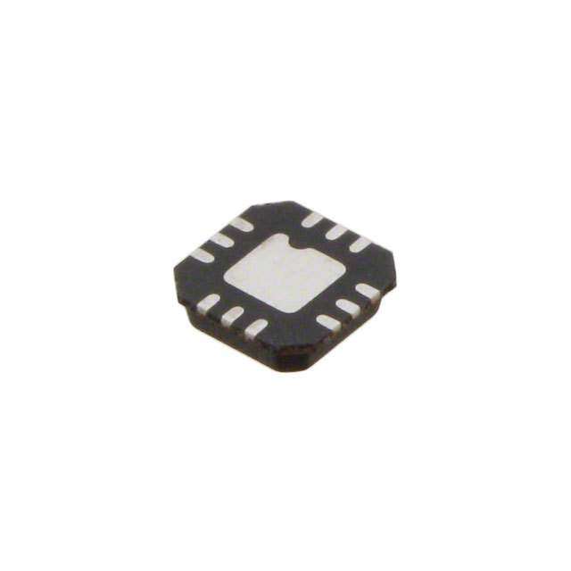
| 产品图片 |
|
| rohs | 符合RoHS无铅 / 符合限制有害物质指令(RoHS)规范要求 |
| 产品系列 | RF集成电路,射频放大器,Skyworks Solutions, Inc. SKY65111-348LF- |
| 数据手册 | |
| P1dB | 29.5 dBm |
| 产品型号 | SKY65111-348LF |
| RF类型 | ISM |
| 产品目录绘图 |
|
| 产品目录页面 | |
| 产品种类 | 射频放大器 |
| 供应商器件封装 | 12-QFN(3x3) |
| 其它名称 | 863-1071-1 |
| 功率增益类型 | 40 dB |
| 包装 | 剪切带 (CT) |
| 商标 | Skyworks Solutions, Inc. |
| 噪声系数 | - |
| 增益 | 40dB |
| 安装风格 | SMD/SMT |
| 封装 | Reel |
| 封装/外壳 | 12-WFQFN 裸露焊盘 |
| 封装/箱体 | QFN-16 |
| 工作电源电压 | 3.5 V |
| 工作频率 | 600 MHz to 1.1 GHz |
| 工厂包装数量 | 3000 |
| 最大工作温度 | + 85 C |
| 最小工作温度 | - 40 C |
| 标准包装 | 1 |
| 测试频率 | 902 MHz to 928 MHz |
| 电压-电源 | 3.5V |
| 电流-电源 | 250mA |
| 电源电流 | 700 mA |
| 类型 | InGaP HBT Power Amplifier |
| 频率 | 600MHz ~ 1.1GHz |


- 商务部:美国ITC正式对集成电路等产品启动337调查
- 曝三星4nm工艺存在良率问题 高通将骁龙8 Gen1或转产台积电
- 太阳诱电将投资9.5亿元在常州建新厂生产MLCC 预计2023年完工
- 英特尔发布欧洲新工厂建设计划 深化IDM 2.0 战略
- 台积电先进制程称霸业界 有大客户加持明年业绩稳了
- 达到5530亿美元!SIA预计今年全球半导体销售额将创下新高
- 英特尔拟将自动驾驶子公司Mobileye上市 估值或超500亿美元
- 三星加码芯片和SET,合并消费电子和移动部门,撤换高东真等 CEO
- 三星电子宣布重大人事变动 还合并消费电子和移动部门
- 海关总署:前11个月进口集成电路产品价值2.52万亿元 增长14.8%


PDF Datasheet 数据手册内容提取
DATA SHEET SKY65111-348LF: ISM 600–1100 MHz Band 2 Watt InGaP HBT Power Amplifier Features Block Diagram ●Optimized for 800–1100 MHz operation VCC2 VCC2 GND Open ●Output power greater than 33 dBm @915 MHz 16 15 14 13 ●3.5 V nominal operating voltage ●Integrated analog power control voltage,VAPC= 0.1–2.8 V GND 1 12 RF OUT/VCC3 ●High PAE at maximum output power ●Ultrasmall,thermally enhanced micro lead frame package. RF IN 2 11 RF OUT/VCC3 ●Low current in standby mode of < 10 µA ●Available on tape and reel ● Available lead (Pb)-free and RoHS-compliant GND 3 10 RF OUT/VCC3 Description VCC1 4 9 RF OUT/VCC3 The SKY65111-348LF is a high-performance 3-stage,high- 5 6 7 8 power amplifier IC designed for use in 600–1100 MHz ISM band applications such as automatic meter readers and RFID.It has an VAPC1 VAPC2 VREF GND integrated analog power control voltage for achieving the desired output power levels.The IC is manufactured on an advanced Package Dimensions InGaP HBT process.The SKY65111-348LF is packaged in a ther- mally enhanced,ultrasmall,micro lead frame package. 0.008 (0.20 mm) Ref. 0.118 Seating Plane NEW Skyworks offers lead (Pb)-free,RoHS (Restriction of (3.00 mm) 0.001 (0.02 mm) Pin 1 ± 0.001 Hazardous Substances)-compliant packaging. Indicator (+0.03 mm -0.02 mm) 0.118 (3.00 mm) 0.030 (0.75 mm) ± 0.002 (0.05 mm) (0.057 (1.45 mm) ± 0.004 (± 0.10 mm) 0.029 (0.73 mm) Exposed Pad 0.029 (0.73 mm) 0.059 (1.500 mm) 0.057 (1.45 mm) ± 0.004 (±0.10 mm) 0.059 (1.500 mm) 0.5 mm Pitch Innovation to GoTM NNBBOOUUWWYY Now available for purchase online. Skyworks Solutions,Inc. • Phone [781] 376-3000 (cid:129) Fax [781] 376-3100 (cid:129) sales@skyworksinc.com (cid:129) www.skyworksinc.com 200428 Rev.E (cid:129) Skyworks Proprietary Information. (cid:129) Products and product information are subject to change without notice. (cid:129) February 12,2007 1
DATA SHEET • SKY65111-348LF Pin Assignments Absolute Maximum Ratings Pin Symbol Description Characteristic Value 1,3, GND Connect this pin to the printed circuit board common Supply voltage (VCC& VREF) 5.5 V 8,14 via lowest possible impedance. Power control voltage (VAPC1 & VAPC2) 3.0 V 2 RF IN RF input port. RF input power 10 dBm 4 VCC1 DC power supply input to the first gain stage. Operating temperature -40 °C to +85 °C 5 VAPC1 Power control voltage input to the first and second gain stages. Storage temperature -65 °C to +85 °C 6 VAPC2 Power control voltage input to the third gain stage. Pnoetr fgourmaraanncteee ids guunadrearn ttheee dfu olln rlayn ugned(se)r dthees ccroibneddit iboyn sth leis Atebds oinlu tthee M sapxeicmifuicmat isopnesc tifaicbalet ioannsd. is 7 VREF Control voltage input to bias control circuit. Exceeding any of the absolute maximum/minimum specifications may result in permanent damage to the device and will void the warranty. 9,10, RF OUT/ RF output ports and DC supply voltage inputs to Each absolute maximum rating listed is an individual parameter.Basing and driving the 11,12 VCC3 third gain stage. amplifier with all absolute maximum ratings listed simultaneously may result in permanent damage to the device. 13 OPEN No connection. Do not connect this pin to ground. 15,16 VCC2 DC power supply input to the second gain stage. CAUTION: Although this device is designed to be as robust as possible,ESD (Electrostatic Discharge) can damage this device.This device must be protected at all times from ESD.Static charges may easily produce poten- tials of several kilovolts on the human body or equipment,which can discharge without detection. Industry-standard ESD precautions must be employed at all times. General DC Electrical Specifications Parameter Symbol Condition Min. Typ. Max. Unit Supply voltage VCC 2.5 3.5 5 V Power control voltage VAPC 0 2.7 2.8 V Power control range 45 dB Power control current IVAPC 5 mA Leakage current PIN< -30 dBm,VAPC1,2 = 0.1 V 10 µA Thermal resistance RTH 50 ° C/W Guaranteed Performance V = 3.5 V,V = 3.5 V,V = 2.7 V,T = 25 °C CC REF APC A Parameter Symbol Condition Specification Unit Critical gain lS21l 902–928 NHz,-30 dBm input 36 min. dB Saturated power PSAT 915 MHz 30 min. dBm Guaranteed performance is as measured in the application’s PC board as defined in this data sheet. Skyworks Solutions,Inc. (cid:129) Phone [781] 376-3000 (cid:129) Fax [781] 376-3100 (cid:129) sales@skyworksinc.com (cid:129) www.skyworksinc.com 2 February 12,2007 (cid:129) Skyworks Proprietary Information (cid:129) Products and Product Information are Subject to Change Without Notice. (cid:129) 200428 Rev.E
DATA SHEET (cid:129) SKY65111-348LF General RF Transmit Electrical Specifications Conditions:V = 3.5 V,V = 3.5 V,V = 2.7 V,P = -30 dBm,T = 25 °C CC REF APC IN A Parameter Symbol Condition Min. Typ. Max. Unit Frequency range F 902 928 MHz Gain lS21l Small signal 40 dB Gain variation over frequency lΔS21l Small signal 0.3 dB Input return loss lS11l Small signal -12 dB Output return loss lS22l Small signal -15 dB Quiescent current ICQ (No RF signal) 0.25 A Output P1 dB P1 dB CW 29.5 dBm Current consumption ICC Output P1 dB 0.7 A Saturated power @ 915 MHz PSAT VCC= 3.5 V,VREF= 3.5 V,VAPC1,2 = 2.7 V 33 dBm Power added efficiency PAE PSAT 50 % Second harmonic F2 Output P1 dB -28 dBm Third harmonic F3 Output P1 dB -38 dBm Ruggedness Output VSWR = 8:1,All phase angles, No module damage VCC= 5 V,PIN= -5 dBm,VAPC= 2.7 V or permanent performance VREF= 5 V degradation Stability Output VSWR = 8:1,All phase angles, -36 dBm VCC= 5 V,PIN= -10 dBm,VAPC= 2.7 V VREF= 5 V Conditions:V = 3.5 V,V = 3.5 V,V = 2.7 V,P = -30 dBm,T = 25 °C CC REF APC IN A Parameter Symbol Condition Min. Typ. Max. Unit Frequency range F 800 1100 MHz Gain lS21l Small signal 39.5 dB Gain variation over frequency lΔS21l Small signal 1.0 dB Input return loss lS11l Small signal -11 dB Output return loss lS22l Smal signal -8 dB Output P1 dB P1 dB CW 27 dBm Quiescent current ICQ (No RF signal) 0.25 A Current consumption ICC Output P1 dB 0.7 A Second harmonic F2 Output P1 dB -17 dBm Third harmonic F3 Output P1 dB -35 dBm Ruggedness Output VSWR = 8:1,All phase angles, No module damage VCC= 5 V,PIN= -5 dBm,VAPC= 2.7 V or permanent performance VREF= 5 V degradation Stability Output VSWR = 8:1,All phase angles,VCC= 5 V, 36 dBm PIN= -10 dBm,VAPC= 2.7 V,VREF= 5 V Saturated power @ 800 MHz PSAT VCC= 3.5 V,VREF= 3.5 V,VAPC1,2 = 2.7 V 32 dBm Power added efficiency @ 800 MHz PAE PSAT 45 % Saturated power @ 1100 MHz PSAT VCC= 3.5 V,VREF= 3.5 V,VAPC1,2 = 2.7 V 30 dBm Power added efficiency @ 1100 MHz PAE PSAT 40 % Unless otherwise stated VREF= VCC. Skyworks Solutions,Inc. (cid:129) Phone [781] 376-3000 (cid:129) Fax [781] 376-3100 (cid:129) sales@skyworksinc.com (cid:129) www.skyworksinc.com 200428 Rev.E (cid:129) Skyworks Proprietary Information. (cid:129) Products and product information are subject to change without notice. (cid:129) February 12,2007 3
DATA SHEET (cid:129) SKY65111-348LF Typical Performance Data VAPC1 Sweep 25 °C VAPC2 Sweep 25 °C 43 800 MHz 915 MHz 1100 MHz VAPC1,2 Sweep 25 °C VAPC1 Sweep -40 °C 42 VAPC2 Sweep -40 °C VAPC1,2 Sweep -40 °C 41 VAPC1 Sweep 85 °C VAPC2 Sweep 85 °C 40 35 VAPC1,2 Sweep 85 °C B) 39 d 25 n ( 38 Gai 37 15 36 m) 5 35 B (dUT -5 34 O 33 P 15 17 19 21 23 25 27 29 31 33 -15 POUT (dBm) -25 Gain vs. P and Frequency OUT -35 V = 3.5, T = 25 °C, V 1,2 = 2.7 V CC APC 0 0.5 1.0 1.5 2.0 2.5 3.0 VAPC (V) P vs. V OUT APC 915 MHz, P = -5 dBm IN VAPC1 varied from 0 V–2.6 V,VAPC2 held at 2.6 V. VAPC2 varied from 0 V–2.6 V,VAPC1 held at 2.6 V. VAPC1 and VAPC2 varied from 0 V–2.6 V together. 800 MHz 915 MHz 1100 MHz 800 MHz 915 MHz 1100 MHz 43 43 42 42 41 41 40 40 B) 39 B) 39 d d n ( 38 n ( 38 Gai 37 Gai 37 36 36 35 35 34 34 33 33 15 17 19 21 23 25 27 29 31 33 15 17 19 21 23 25 27 29 31 33 POUT (dBm) POUT (dBm) Gain vs. P and Frequency Gain vs. P and Frequency OUT OUT V = 3.5, T = 25 °C, V 1,2 = 2.8 V V = 3.5, T = 25 °C, V 1,2 = 2.6 V CC APC CC APC Skyworks Solutions,Inc. (cid:129) Phone [781] 376-3000 (cid:129) Fax [781] 376-3100 (cid:129) sales@skyworksinc.com (cid:129) www.skyworksinc.com 4 February 12,2007 (cid:129) Skyworks Proprietary Information (cid:129) Products and Product Information are Subject to Change Without Notice. (cid:129) 200428 Rev.E
DATA SHEET (cid:129) SKY65111-348LF 25 °C 85 °C -40 °C 43 VCC = 5 V VCC = 3.5 V VCC = 2.5 V -20 °C 50 °C 0 °C 43 42 42 41 41 40 B) 40 d B) 39 n ( 39 n (d 38 Gai 38 Gai 37 37 36 35 36 34 35 33 15 17 19 21 23 25 27 29 31 33 35 37 15 17 19 21 23 25 27 29 31 33 POUT (dBm) POUT (dBm) Gain vs. P , V 1, 2 = 2.7 V, OUT APC Gain vs. POUT, VCC = 3.5, 915 MHz @ 25 °C V 1, 2 = 2.7 V, 915 MHz APC VAPC1,2 = 2.7 V VCC = 3.5 V, VAPC1,2 = 2.7 V VAPC1,2 = 2.6 V VCC = 3.5 V, VAPC1,2 = 2.6 V VAPC1,2 = 2.8 V VCC = 3.5 V, VAPC1,2 = 2.8 V -15 VCC = 4 V, VAPC1,2 = 2.6 V VCC = 4 V, VAPC1,2 = 2.7 V -20 VCC = 4 V, VAPC1,2 = 2.8 V 55 -25 50 m) 45 B (dO -30 40 2F 35 P -35 %) 30 E ( 25 -40 PA 20 15 -45 15 17 19 21 23 25 27 29 31 33 35 10 5 POUT (dBm) 0 2F0 vs. POUT, 915 MHz Fundamental, VCC = 3.5 V 10 12 14 16 18 20 22 24 26 28 30 32 34 36 25 °C POUT (dBm) % PAE vs. V 1, 2, and V APC CC 915 MHz @ 25 °C Skyworks Solutions,Inc. (cid:129) Phone [781] 376-3000 (cid:129) Fax [781] 376-3100 (cid:129) sales@skyworksinc.com (cid:129) www.skyworksinc.com 200428 Rev.E (cid:129) Skyworks Proprietary Information. (cid:129) Products and product information are subject to change without notice. (cid:129) February 12,2007 5
DATA SHEET (cid:129) SKY65111-348LF VCC = 3.5 V, VAPC1,2 = 2.7 V VCC = 3.5 V, VAPC = 2.7 V VCC = 3.5 V, VAPC = 2.6 V VCC = 2.5 V, VAPC1,2 = 2.7 V VCC = 3.5 V, VAPC = 2.8 V VCC = 4 V, VAPC = 2.6 V VCC = 4 V, VAPC1,2 = 2.7 V VCC = 4 V, VAPC = 2.7 V VCC = 4 V, VAPC = 2.8 V 1.5 65 VCC = 5 V, VAPC1,2 = 2.7 V 1.4 60 1.3 55 1.2 1.1 50 1.0 45 0.9 %) 3450 (A) C 00..78 E ( 30 IC 0.6 A P 25 0.5 20 0.4 0.3 15 0.2 10 0.1 5 0 0 12 14 16 18 20 22 24 26 28 30 32 34 36 10 12 14 16 18 20 22 24 26 28 30 32 34 36 38 POUT (dBm) POUT (dBm) I vs. P , V and V 1,2 CC OUT CC APC % PAE vs. P and V , OUT CC 915 MHz, 25 °C V 1,2 = 2.7, 915 MHz @ 25 °C APC VCC = 3.5 V, VAPC = 2.7 V VCC = 2.5V, VAPC = 2.7 V 25 °C -40 °C -20 °C 1.8 VCC = 4 V, VAPC = 2.7 V VCC = 5 V, VAPC = 2.7 V 500 0 °C 50 °C 85 °C 1.6 450 1.4 400 350 1.2 (A) CC 01..80 (mA) Q 235000 I C 200 0.6 I 150 0.4 100 0.2 50 0 0 14 16 18 20 22 24 26 28 30 32 34 36 38 2.60 2.65 2.70 2.75 2.80 POUT (dBm) VAPC1,2 (V) I vs. P and V , V 1,2 = 2.7 V, I vs V 1, 2, V = 3.5 V CC OUT CC APC CQ APC CC 915 MHz @ 25 °C RF Off @ 25 °C Skyworks Solutions,Inc. (cid:129) Phone [781] 376-3000 (cid:129) Fax [781] 376-3100 (cid:129) sales@skyworksinc.com (cid:129) www.skyworksinc.com 6 February 12,2007 (cid:129) Skyworks Proprietary Information (cid:129) Products and Product Information are Subject to Change Without Notice. (cid:129) 200428 Rev.E
DATA SHEET (cid:129) SKY65111-348LF 915 MHz 800 MHz VCC = 3.5 V VCC = 2.5 V VCC = 5 V 50 1000 MHz 1100 MHz 41 40 30 40 20 39 B) 10 Bm) n (d 0 3 (d 38 Gai -10 OIP -20 37 -30 36 -40 -50 35 0.2 0.4 0.6 0.8 1.0 1.2 1.4 1.6 1.8 2.0 2.2 2.4 2.6 2.8 2.60 2.65 2.70 2.75 2.80 2.85 2.90 2.95 3.00 Frequency (GHz) VAPC (V) Gain vs. Frequency, V 1, 2 = 2.7 V APC OIP3 vs. VAPC1,2, Tone Spacing 1 MHz PIN = -30 dBm, 25 °C V = 3.5 V P = 20 dBm @ 25 °C CC OUT 25 °C -40 °C -20 °C 25 °C -40 °C -20 °C 0 °C 50 °C 85 °C 0 °C 50 °C 85 °C 50 0 40 -5 30 B) 20 s (d -10 B) 10 Los n (d 0 urn -15 Gai -10 Ret -20 ut -20 p n -30 I -25 -40 -50 -30 0.2 0.4 0.6 0.8 1.0 1.2 1.4 1.6 1.8 2.0 2.2 2.4 2.6 2.8 0.2 0.4 0.6 0.8 1.0 1.2 1.4 1.6 1.8 2.0 2.2 2.4 2.6 2.8 Frequency (GHz) Frequency (GHz) Gain vs. Frequency, V = 3.5 V, Input Return Loss vs. Frequenc CC PIN = -30 dBm, VAPC1,2 = 2.7 V VCC = 3.5 V, PIN = -30 dBm, VAPC1,2 = 2.7 V Skyworks Solutions,Inc. (cid:129) Phone [781] 376-3000 (cid:129) Fax [781] 376-3100 (cid:129) sales@skyworksinc.com (cid:129) www.skyworksinc.com 200428 Rev.E (cid:129) Skyworks Proprietary Information. (cid:129) Products and product information are subject to change without notice. (cid:129) February 12,2007 7
DATA SHEET (cid:129) SKY65111-348LF 25 °C -40 °C -20 °C 25 °C -40 °C -20 °C 0 °C 50 °C 85 °C 0 °C 50 °C 85 °C 0 0 -5 -10 oss (dB) ---211050 on (dB) ---432000 urn L -25 solati -50 Output Ret ---433050 Reverse I ---876000 -45 -90 -50 -100 0.2 0.4 0.6 0.8 1.0 1.2 1.4 1.6 1.8 2.0 2.2 2.4 2.6 2.8 0.2 0.4 0.6 0.8 1.0 1.2 1.4 1.6 1.8 2.0 2.2 2.4 2.6 2.8 Frequency (GHz) Frequency (GHz) Output Return Loss vs. Frequency, V = 3.5 V Reverse Isolation vs. Frequency, V = 3.5 V CC CC P = -30 dBm, V 1,2 = 2.7 V P = -30 dBm, V 1,2 = 2.7 V IN APC IN APC 25 °C -40 °C -20 °C 25 °C -40 °C -20 °C 0 °C 50 °C 85 °C 0 °C 50 °C 85 °C 45 0 44 43 -5 42 41 dB) 40 s ( -10 Gain (dB) 33336789 Return Los -15 35 ut -20 34 p n 33 I -25 32 31 30 -30 0.80 0.84 0.88 0.92 0.96 1.00 1.04 1.081.10 0.80 0.84 0.88 0.92 0.96 1.00 1.04 1.081.10 Frequency (GHz) Frequency (GHz) Gain vs. Frequency, VCC = 3.5 V Input Return Loss vs. Frequency, VCC = 3.5 V PIN = -30 dBm, VAPC1,2 = 2.7 V PIN = -30 dBm, VAPC1,2 = 2.7 V Skyworks Solutions,Inc. (cid:129) Phone [781] 376-3000 (cid:129) Fax [781] 376-3100 (cid:129) sales@skyworksinc.com (cid:129) www.skyworksinc.com 8 February 12,2007 (cid:129) Skyworks Proprietary Information (cid:129) Products and Product Information are Subject to Change Without Notice. (cid:129) 200428 Rev.E
DATA SHEET (cid:129) SKY65111-348LF 25 °C -40 °C -20 °C 25 °C -40 °C -20 °C 0 °C 50 °C 85 °C 0 °C 50 °C 85 °C 0 0 -5 -10 dB) -10 B) -20 Return Loss ( ----32210505 e Isolation (d ----65430000 put -35 vers -70 Out -40 Re -80 -45 -90 -50 -100 0.80 0.84 0.88 0.92 0.96 1.00 1.04 1.081.10 0.80 0.84 0.88 0.92 0.96 1.00 1.04 1.081.10 Frequency (GHz) Frequency (GHz) Output Return Loss vs. Frequency, VCC = 3.5 V Reverse Isolation vs. Frequency, VCC = 3.5 V PIN = -30 dBm, VAPC1,2 = 2.7 V PIN = -30 dBm, VAPC1,2 = 2.7 V VCC = 3.5 V @ 855 KHz VCC = 4 V @ 855 KHz VCC = 3.5 V @ 855 KHz VCC = 4 V @ 855 KHz VCC = 2.5 V @ 855 KHz VCC = 3.5 V @ 1.98 MHz VCC = 2.5 V @ 855 KHz VCC = 3.5 V @ 1.98 MHz VCC = 4 V @ 1.98 MHz VCC = 2.5 V @ 1.98 MHz VCC = 4 V @ 1.98 MHz VCC = 2.5 V @ 1.98 MHz VCC = 5 V @ 855 KHz VCC = 5 V @ 1.98 MHz VCC = 5 V @ 855 KHz VCC = 5 V @ 1.98 MHz -40 -40 -45 -45 -50 -50 c) c) B B d d R ( -55 R ( -55 P P C C A -60 A -60 -65 -65 -70 -70 15 16 17 18 19 20 21 22 23 24 25 26 27 28 15 16 17 18 19 20 21 22 23 24 25 26 27 28 POUT (dBm) POU T (dBm) ACPR vs, P and Frequency ACPR vs, P and Frequency OUT OUT IS-95, V 1,2 = 2.7 V, 881 MHz @ 25 °C IS-95, V 1,2 = 2.7 V, 836 MHz @ 25 °C APC APC Skyworks Solutions,Inc. (cid:129) Phone [781] 376-3000 (cid:129) Fax [781] 376-3100 (cid:129) sales@skyworksinc.com (cid:129) www.skyworksinc.com 200428 Rev.E (cid:129) Skyworks Proprietary Information. (cid:129) Products and product information are subject to change without notice. (cid:129) February 12,2007 9
DATA SHEET (cid:129) SKY65111-348LF ACPR,IS-95 REV,V 3.5 V,V 1,2 = 2.7 V ACPR,IS-95 FWD,V 3.5 V,V 1,2 = 2.7 V CC APC CC APC 881 MHz @ 25 °C 836 MHz @ 25 °C Response Time,P = -15 dBm,915 MHz,V = 3.5 V, Response Time,Rise Time,50% Ctrl,90% RF IN CC V 1,2 = 2.7 V @ 25 °C V 1,2 = 2.7 V/0 V @ 25 °C APC APC Response Time,Fall Time 90% RF,50% Ctrl V 1,2 = 2.7 V/0 V @ 25 °C APC Skyworks Solutions,Inc. (cid:129) Phone [781] 376-3000 (cid:129) Fax [781] 376-3100 (cid:129) sales@skyworksinc.com (cid:129) www.skyworksinc.com 10 February 12,2007 (cid:129) Skyworks Proprietary Information (cid:129) Products and Product Information are Subject to Change Without Notice. (cid:129) 200428 Rev.E
DATA SHEET (cid:129) SKY65111-348LF Bill of Material for Evaluation Board Designator Value Size Manufacturer Part Number Notes C1 100 pF 0402 Murata GRM1555C1H101JD83E C2 2.2 pF 0402 Murata GRM1555C1H2R2JZ35E C3 4.7 pF 0402 Murata GRM1555C1H4R7JZ35E C4 100 pF 0402 Murata GRM1555C1H101JD83E C5 1000 pF 0402 Murata GRM155R71H102KA01 1 C7 DNP 2 C8 100 pF 0402 Murata GRM1555C1H101JD83E C9 1000 pF 0402 Murata GRM155R71H102KA01 1 C10 10 µF 0402 AVX TAJA106M006R C11 100 pF 0402 Murata GRM1555C1H101JD83E 1 C12 1000 pF 0402 Murata GRM155R71H102KA01 1 C13 10 nF 0402 Murata GRM155R71E103KA01 1 C14 10 µF 1206 AVX TAJA106M006R C15 12 pF 0402 Murata GJM1555C1H120JB01E C16 5.6 pF 0402 Murata GJM1555C1H5R6CB01E C17 10 µF 1206 AVX TAJA106M006R C18 DNP 2 C19 DNP 2 C20 DNP 2 C21 DNP 2 C22 1000 pF 0402 Murata GRM155R71H102KA01 C23 100 pF 0402 Murata GRM1555C1H101JD83E C24 100 pF 0402 Murata GRM1555C1H101JD83E C25 18 pF 0402 Murata GRM1555C180JZ35E L1 1.8 nH 0402 Johanson L-07C1N8ST L2 1 nH 0402 Johanson L-07C1N0ST R1 0 W 0402 Panasonic ERJ2BJ00X 1 R2 0 W 0402 Panasonic ERJ2BJ00X 1 1.Panasonic and Murata are Skyworks preferred vendors. However,any suitable equivalent part is acceptable for this component. 2."DNP" = Do not place. Skyworks Solutions,Inc. (cid:129) Phone [781] 376-3000 (cid:129) Fax [781] 376-3100 (cid:129) sales@skyworksinc.com (cid:129) www.skyworksinc.com 200428 Rev.E (cid:129) Skyworks Proprietary Information. (cid:129) Products and product information are subject to change without notice. (cid:129) February 12,2007 11
DATA SHEET (cid:129) SKY65111-348LF Application Circuit VCC2 C10 C9 C8 C7 C11 C12 C13 C14 VCC3 16 15 14 13 1 12 L1 2 11 RF In C1 C25 SKY65111-348 C2 3 10 C15 C16 C24 RF Out C3 4 9 5 6 7 8 L2 VCC1 C17 C5 C4 C18 C19 C23 C22 VREF R1 R2 VAPC1 VAPC2 C20 C21 Component Placement Diagram Transmission line width:0.027 inches. Gerber files available upon request. Incorrect soldering of the device paddle to grounding pad may lead to parasitic oscillations,reduced performance and increased device temperature rise.Uniform coverage over the entire bottom ground paddle must be maintained to avoid these conditions. Skyworks Solutions,Inc. (cid:129) Phone [781] 376-3000 (cid:129) Fax [781] 376-3100 (cid:129) sales@skyworksinc.com (cid:129) www.skyworksinc.com 12 February 12,2007 (cid:129) Skyworks Proprietary Information (cid:129) Products and Product Information are Subject to Change Without Notice. (cid:129) 200428 Rev.E
DATA SHEET (cid:129) SKY65111-348LF Application Circuit Notes V (Pin 7).V is the bias reference voltage for amplifier REF REF stages 2 and 3.V should be operated over the same voltage Ground,(Pins 1,3,8,14).Attach all ground pins to the RF REF range as V ,with a nominal voltage of 3.5 V .Bypassing of ground plane with the largest diameter and lowest inductance via CC DC V is accomplished with C22 and C23 which should be placed that the layout will allow.Multiple small vias are also acceptable REF as close to the device pin as possible. and will work well under the device if solder migration is an issue.It is extremely important that the device paddle be suffi- RF ,V 3 (Pins 9-12).RF and V 3 are the biasing input of OUT CC OUT CC ciently grounded for both thermal and stability reasons.Please the stage 3 collectors.Bias is applied to the RF output through a refer to the enclosed Package Footprint. length of transmission line that is approximately 827 mils (21 mm) long.Capacitors C11-C14 provide proper RF bypassing and RF input (Pin 2).A lumped element matching structure for good should be placed as shown in the Applications Circuit.Output in-band return loss has been realized on the RF input,Pin 2.This matching for optimal power gain is accomplished with capacitors structure is comprised of a DC blocking capacitor (C1),low pass C15 and C16.Spacing between these capacitors with respect to LC filter (L1,C1) and at the device input,a series capacitor (C25). the RF output and each other is critical and is shown on the This combination of devices will yield a return loss better than - Component Placement Diagram.Special care must be taken 11 dB over the entire 800–1100 MHz band of interest.The when placing these devices; their locations should not deviate placement of C1 is not critical; it can be moved as close to L1, significantly from the locations as shown.If these capacitors are C2 and C25 as desired.C25 should be placed as close to the not located properly,large decreases in output power and effi- device pin as possible to replicate performance as measured on ciency will occur. the applications board. Pin 13.Pin 13 has no connection and should be left open circuit. V 1 (Pin 4).V 1 is the collector bias for the first amplifier CC CC stage in the SKY65111.Multiple bypass capacitors,C3-C5,C17 V 2 (Pins 15-16).V 2 is the collector bias input for the second CC CC and a series inductor,L2,have been utilized to ensure stability amplifier stage in the SKY65111.Multiple bypass capacitors, both in and out of the useable bandwidth of the device.The C8-C10 have been utilized to ensure stability both in and out of length of transmission line between L2 and Pin 4 is not critical; the useable bandwidth of the device.Capacitor C7 is not popu- L2 can be placed as close to the pin as possible if desired. lated with the normal tuning configuration described above. However,placement of L2 farther away from Pin 4 than shown on the Applications Circuit is not recommended.C3 should also be placed in the approximate location shown on the Applications Circuit,but placement is not critical. V 1 (Pin 5).V 1 is the bias control voltage input for amplifier APC APC stages 1 and 2.Nominal operating range is between 2.6 V and DC 2.8 V ,with 3 V producing the minimum attenuation point. DC DC V 1 may also be set to 0 V ,to force stages 1 and 2 into APC DC standby mode. V 2 (Pin 6).V 2 is the bias control voltage for amplifier APC APC stage 3.Nominal operating range is between 2.6 V and DC 2.8 V ,with 3 V producing the minimum attenuation point. DC DC A 100 pF capacitor (C19) may be used for bypassing at high frequencies.The value of this capacitor may also be made large, greater than 1000 pF,if longer response time is acceptable. V 2 may also be set to 0 V ,to place amplifier stage 3 into APC DC standby status. NOTE:In most applications V 1 and V 2 pins are directly tied APC APC together and biased from the same control voltage.V 1 APC and V 2 may also be split if independent control is APC desired. Skyworks Solutions,Inc. (cid:129) Phone [781] 376-3000 (cid:129) Fax [781] 376-3100 (cid:129) sales@skyworksinc.com (cid:129) www.skyworksinc.com 200428 Rev.E (cid:129) Skyworks Proprietary Information. (cid:129) Products and product information are subject to change without notice. (cid:129) February 12,2007 13
DATA SHEET (cid:129) SKY65111-348LF Package Footprint Evaluation Board Stack-Up Via Plating Thru Both Boards Circuit Board See Note 3 See Note 1A 0.014 0.062 Ref. ± 0.002 Ref. Copper Side Circuit Board Backing of Backing See Note 1B Detail A Skyworks Solutions,Inc. (cid:129) Phone [781] 376-3000 (cid:129) Fax [781] 376-3100 (cid:129) sales@skyworksinc.com (cid:129) www.skyworksinc.com 14 February 12,2007 (cid:129) Skyworks Proprietary Information (cid:129) Products and Product Information are Subject to Change Without Notice. (cid:129) 200428 Rev.E
DATA SHEET (cid:129) SKY65111-348LF Application Board Bias Procedure 1 GND 2 Step 1.Connect DC ground. Step 2.Connect all V and V lines to 3.5 V supply,labeled 2. CC REF Step 3.With the RF off,apply 2.7 V to V 1,2 control pins. DC APC Verify the I current is approximately 250 mA,labeled 3. CQ Step 4.Apply RF signal data -30 dBm level and observe that the output level is approximately 10 dBm or the gain of the device is approximately 40 dB. NOTE: It is important that the V 1,V 2,V 3,and V voltage RF In RF Out CC CC CC REF source be adjusted such that 3.5 V is measured at the board.The high collector currents will drop the collector voltage significantly if long leads are used.Adjust the bias voltage to compensate. Recommended Solder Reflow Profiles Refer to the “Recommended Solder Reflow Profile” 1 GND 3 1 GND Application Note. 2 Tape and Reel Information Branding Specifications Refer to the “Discrete Devices and IC Switch/Attenuators Tape and Reel Package Orientation” Application Note. Pin 1 Pin 16 Indicator S111 Skyworks P/N Pin 1 XXXX Lot # YWW Date Code Y = Calendar Year WW = Week Top View Skyworks Solutions,Inc. (cid:129) Phone [781] 376-3000 (cid:129) Fax [781] 376-3100 (cid:129) sales@skyworksinc.com (cid:129) www.skyworksinc.com 200428 Rev.E (cid:129) Skyworks Proprietary Information. (cid:129) Products and product information are subject to change without notice. (cid:129) February 12,2007 15
DATA SHEET (cid:129) SKY65111-348LF Copyright © 2002,2003,2004,2005,2006,2007,Skyworks Solutions,Inc.All Rights Reserved. Information in this document is provided in connection with Skyworks Solutions,Inc.(“Skyworks”) products or services.These materials,including the information contained herein,are provided by Skyworks as a service to its customers and may be used for informational purposes only by the customer.Skyworks assumes no responsibility for errors or omissions in these materials or the information contained herein.Skyworks may change its documentation,products,services,specifications or product descriptions at any time,without notice.Skyworks makes no commitment to update the materials or information and shall have no responsibility whatsoever for conflicts,incompatibilities,or other difficulties arising from any future changes. No license,whether express,implied,by estoppel or otherwise,is granted to any intellectual property rights by this document.Skyworks assumes no liability for any materials,products or information provided hereunder,including the sale,distribution,reproduction or use of Skyworks products,information or materials,except as may be provided in Skyworks Terms and Conditions of Sale. THE MATERIALS,PRODUCTS AND INFORMATION ARE PROVIDED “AS IS”WITHOUT WARRANTY OF ANY KIND,WHETHER EXPRESS,IMPLIED,STATUTORY,OR OTHERWISE,INCLUDING FITNESS FOR A PARTICULAR PURPOSE OR USE,MERCHANTABILITY,PERFORMANCE,QUALITY OR NON-INFRINGEMENT OF ANY INTELLECTUAL PROPERTY RIGHT; ALL SUCH WARRANTIES ARE HEREBY EXPRESSLY DISCLAIMED.SKYWORKS DOES NOT WARRANT THE ACCURACY OR COMPLETENESS OF THE INFORMATION,TEXT,GRAPHICS OR OTHER ITEMS CONTAINED WITHIN THESE MATERIALS.SKYWORKS SHALL NOT BE LIABLE FOR ANY DAMAGES,INCLUDING BUT NOT LIMITED TO ANY SPECIAL,INDIRECT,INCIDENTAL,STATUTORY,OR CONSEQUENTIAL DAMAGES,INCLUDING WITHOUT LIMITATION, LOST REVENUES OR LOST PROFITS THAT MAY RESULT FROM THE USE OF THE MATERIALS OR INFORMATION,WHETHER OR NOT THE RECIPIENT OF MATERIALS HAS BEEN ADVISED OF THE POSSIBILITY OF SUCH DAMAGE. Skyworks products are not intended for use in medical,lifesaving or life-sustaining applications,or other equipment in which the failure of the Skyworks products could lead to personal injury, death,physical or environmental damage.Skyworks customers using or selling Skyworks products for use in such applications do so at their own risk and agree to fully indemnify Skyworks for any damages resulting from such improper use or sale. Customers are responsible for their products and applications using Skyworks products,which may deviate from published specifications as a result of design defects,errors,or operation of products outside of published parameters or design specifications.Customers should include design and operating safeguards to minimize these and other risks.Skyworks assumes no liability for applications assistance,customer product design,or damage to any equipment resulting from the use of Skyworks products outside of stated published specifications or parameters. Skyworks,the Skyworks symbol,and “Breakthrough Simplicity”are trademarks or registered trademarks of Skyworks Solutions,Inc.,in the United States and other countries.Third-party brands and names are for identification purposes only,and are the property of their respective owners.Additional information,including relevant terms and conditions,posted at www.skyworksinc.com,are incorporated by reference. Skyworks Solutions,Inc. (cid:129) Phone [781] 376-3000 (cid:129) Fax [781] 376-3100 (cid:129) sales@skyworksinc.com (cid:129) www.skyworksinc.com 16 February 12,2007 (cid:129) Skyworks Proprietary Information (cid:129) Products and Product Information are Subject to Change Without Notice. (cid:129) 200428 Rev.E