ICGOO在线商城 > 射频/IF 和 RFID > RF 放大器 > ADL5531ACPZ-R7
 Datasheet下载
- 型号: ADL5531ACPZ-R7
- 制造商: Analog
- 库位|库存: xxxx|xxxx
- 要求:
| 数量阶梯 | 香港交货 | 国内含税 |
| +xxxx | $xxxx | ¥xxxx |
查看当月历史价格
查看今年历史价格
ADL5531ACPZ-R7产品简介:
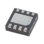
ICGOO电子元器件商城为您提供ADL5531ACPZ-R7由Analog设计生产,在icgoo商城现货销售,并且可以通过原厂、代理商等渠道进行代购。 ADL5531ACPZ-R7价格参考¥12.17-¥15.22。AnalogADL5531ACPZ-R7封装/规格:RF 放大器, RF Amplifier IC W-CDMA, CDMA, GSM, UMTS 20MHz ~ 500MHz 8-LFCSP-VD (3x3)。您可以下载ADL5531ACPZ-R7参考资料、Datasheet数据手册功能说明书,资料中有ADL5531ACPZ-R7 详细功能的应用电路图电压和使用方法及教程。
ADL5531ACPZ-R7是Analog Devices Inc.生产的一款RF放大器,属于高性能、低功耗的增益模块,主要应用于射频信号放大。其典型应用场景包括无线通信基础设施,如蜂窝基站中的中频(IF)和射频(RF)信号链路,适用于GSM、CDMA、WCDMA、LTE等多种通信标准。该器件工作频率范围宽(可达100 MHz至4000 MHz),适合多频段射频系统设计。

ADL5531ACPZ-R7常用于驱动高速模数转换器(ADC)的前端,作为缓冲放大器,提升信号完整性。同时,也广泛应用于点对点微波通信、宽带无线接入系统(如WiMAX)、有线电视(CATV)基础设施以及测试与测量设备中,提供稳定、低噪声的信号放大功能。

该芯片采用紧凑型16引脚LFCSP封装,便于高密度PCB布局,并具备良好的线性度和输出功率(典型输出P1dB为+17 dBm),支持单端输入输出,简化系统设计。其内部集成了偏置控制电路,确保温度稳定性,适合在工业温度范围内可靠运行。

综上,ADL5531ACPZ-R7是一款适用于高性能射频系统的关键元件,广泛用于通信设备、信号发生器、接收机前端及各类宽带射频放大场合。
| 参数 | 数值 |
| 产品目录 | |
| 描述 | IC IF GAIN BLOCK 500MHZ 8LFCSP射频放大器 20-500MHz IF Gain Block |
| DevelopmentKit | ADL5531-EVALZ |
| 产品分类 | |
| 品牌 | Analog Devices Inc |
| 产品手册 | |
| 产品图片 |
|
| rohs | 符合RoHS无铅 / 符合限制有害物质指令(RoHS)规范要求 |
| 产品系列 | RF集成电路,射频放大器,Analog Devices ADL5531ACPZ-R7- |
| 数据手册 | |
| P1dB | 20.4dBm(109.6mW) |
| 产品型号 | ADL5531ACPZ-R7 |
| PCN其它 | |
| RF类型 | W-CDMA,CDMA,GSM,UMTS |
| 产品培训模块 | http://www.digikey.cn/PTM/IndividualPTM.page?site=cn&lang=zhs&ptm=24737 |
| 产品目录页面 | |
| 产品种类 | 射频放大器 |
| 供应商器件封装 | 8-LFCSP-VD(3x3) |
| 其它名称 | ADL5531ACPZ-R7CT |
| 功率增益类型 | 19.7 dB |
| 包装 | 剪切带 (CT) |
| 商标 | Analog Devices |
| 噪声系数 | 3dB |
| 增益 | 19.2dB ~ 20.5dB |
| 安装风格 | SMD/SMT |
| 封装 | Reel |
| 封装/外壳 | 8-VFDFN 裸露焊盘,CSP |
| 封装/箱体 | LFCSP-8 |
| 工作电源电压 | 5 V |
| 工作频率 | 20 MHz to 500 MHz |
| 工厂包装数量 | 1500 |
| 最大功率耗散 | 600 mW |
| 最大工作温度 | + 85 C |
| 最小工作温度 | - 40 C |
| 标准包装 | 1 |
| 测试频率 | 380MHz |
| 特色产品 | http://www.digikey.com/cn/zh/ph/analog-devices/rf.html |
| 电压-电源 | 4.75 V ~ 5.25 V |
| 电流-电源 | 100mA ~ 110mA |
| 电源电流 | 100 mA |
| 类型 | IFA |
| 系列 | ADL5531 |
| 视频文件 | http://www.digikey.cn/classic/video.aspx?PlayerID=1364138032001&width=640&height=505&videoID=2245193150001 |
| 输入返回损失 | - 19.5 dB |
| 输出截获点 | 36 dBm |
| 通道数量 | 1 Channel |
| 隔离分贝 | - 23 dB |
| 频率 | 20MHz ~ 500MHz |


- 商务部:美国ITC正式对集成电路等产品启动337调查
- 曝三星4nm工艺存在良率问题 高通将骁龙8 Gen1或转产台积电
- 太阳诱电将投资9.5亿元在常州建新厂生产MLCC 预计2023年完工
- 英特尔发布欧洲新工厂建设计划 深化IDM 2.0 战略
- 台积电先进制程称霸业界 有大客户加持明年业绩稳了
- 达到5530亿美元!SIA预计今年全球半导体销售额将创下新高
- 英特尔拟将自动驾驶子公司Mobileye上市 估值或超500亿美元
- 三星加码芯片和SET,合并消费电子和移动部门,撤换高东真等 CEO
- 三星电子宣布重大人事变动 还合并消费电子和移动部门
- 海关总署:前11个月进口集成电路产品价值2.52万亿元 增长14.8%


PDF Datasheet 数据手册内容提取
20 MHz to 500 MHz IF Gain Block Data Sheet ADL5531 FEATURES FUNCTIONAL BLOCK DIAGRAM Fixed gain of 20 dB ADL5531 Operation up to 500 MHz NC 1 8NC Input/output internally matched to 50 Ω RFIN 2 7RFOUT Integrated bias control circuit BIAS NC 3 CONTROL 6NC Output IP3 NC 4 LINEARIZER 5CLIN 41 dBm at 70 MHz Ou3t9p udtB 1m d aBt c1o9m0 pMrHeszs ion: 20.6 dB at 190 MHz NC = NO CONNECT 06833-001 Figure 1. Noise figure: 2.5 dB at 190 MHz Single 5 V power supply Small footprint 8-lead LFCSP ADL5534 20 dB gain dual-channel version ±2 kV ESD (Class 2) GENERAL DESCRIPTION The ADL5531 is a broadband, fixed-gain, linear amplifier The ADL5531 is fabricated on a GaAs HBT process and has that operates at frequencies up to 500 MHz. The device can be an ESD rating of ±2 kV (Class 2). The device is packaged in an used in a wide variety of equipment, including cellular, satellite, 8-lead 3 mm × 3 mm LFCSP that uses an exposed paddle for broadband, and instrumentation equipment. excellent thermal impedance. The ADL5531 provides a gain of 20 dB, which is stable over The ADL5531 consumes 100 mA on a single 5 V supply and is frequency, temperature, power supply, and from device to device. fully specified for operation from −40°C to +85°C. This amplifier is single ended and internally matched to 50 Ω. The dual-channel 20 dB gain version, ADL5534, is also available Only input/output ac coupling capacitors, power supply decoupling from Analog Devices, Inc. capacitors, and external inductors are required for operation. Rev. C Document Feedback Information furnished by Analog Devices is believed to be accurate and reliable. However, no responsibility is assumed by Analog Devices for its use, nor for any infringements of patents or other One Technology Way, P.O. Box 9106, Norwood, MA 02062-9106, U.S.A. rights of third parties that may result from its use. Specifications subject to change without notice. No license is granted by implication or otherwise under any patent or patent rights of Analog Devices. Tel: 781.329.4700 ©2007–2017 Analog Devices, Inc. All rights reserved. Trademarks and registered trademarks are the property of their respective owners. Technical Support www.analog.com
ADL5531 Data Sheet TABLE OF CONTENTS Features .............................................................................................. 1 Typical Performance Characteristics ..............................................7 Functional Block Diagram .............................................................. 1 Basic Connections .............................................................................9 General Description ......................................................................... 1 Soldering Information and Recommended PCB Land Revision History ............................................................................... 2 Pattern .............................................................................................9 Specifications ..................................................................................... 3 Evaluation Board ............................................................................ 10 Typical Scattering Parameters ..................................................... 4 Outline Dimensions ....................................................................... 11 Absolute Maximum Ratings ............................................................ 5 Ordering Guide .......................................................................... 11 ESD Caution .................................................................................. 5 Pin Configuration and Function Descriptions ............................. 6 REVISION HISTORY 8/2017—Rev. B to Rev. C Changed CP-8-2 to CP-8-13 ........................................ Throughout Updated Outline Dimensions ....................................................... 11 Changes to Ordering Guide .......................................................... 11 11/2013—Rev. A to Rev. B Changes to Figure 2 .......................................................................... 6 Added Figure 14, Renumbered Sequentially ................................ 8 8/2008—Rev. 0 to Rev. A Changes to Features Section and General Description Section ................................................................................................ 1 Added Exposed Pad Notation to Outline Dimensions ............. 11 8/2007—Revision 0: Initial Version Rev. C | Page 2 of 12
Data Sheet ADL5531 SPECIFICATIONS VPOS = 5 V and T = 25°C, unless otherwise noted. A Table 1. Parameter Conditions Min Typ Max Unit OVERALL FUNCTION Frequency Range 20 500 MHz Gain (S21) 190 MHz 20.3 dB Input Return Loss (S11) 190 MHz −19.5 dB Output Return Loss (S22) 190 MHz −26.5 dB Reverse Isolation (S12) 190 MHz −23.0 dB FREQUENCY = 70 MHz Gain 20.9 dB vs. Frequency ± 5 MHz ±0.03 dB vs. Temperature −40°C ≤ T ≤ +85°C ±0.22 dB A vs. Supply 4.75 V to 5.25 V ±0.19 dB Output 1 dB Compression Point 20.4 dBm Output Third-Order Intercept Δf = 1 MHz, output power (P ) = 0 dBm per tone 41.0 dBm OUT Noise Figure 2.5 dB FREQUENCY = 190 MHz Gain 19.7 20.3 21.0 dB vs. Frequency ± 50 MHz ±0.12 dB vs. Temperature −40°C ≤ T ≤ +85°C ±0.22 dB A vs. Supply 4.75 V to 5.25 V ±0.17 dB Output 1 dB Compression Point 20.6 dBm Output Third-Order Intercept Δf = 1 MHz, output power (P ) = 0 dBm per tone 39.0 dBm OUT Noise Figure 2.5 dB FREQUENCY = 380 MHz Gain 19.2 19.7 20.5 dB vs. Frequency ± 50 MHz ±0.15 dB vs. Temperature −40°C ≤ T ≤ +85°C ±0.24 dB A vs. Supply 4.75 V to 5.25 V ±0.15 dB Output 1 dB Compression Point 20.4 dBm Output Third-Order Intercept Δf = 1 MHz, output power (P ) = 0 dBm per tone 36.0 dBm OUT Noise Figure 3.0 dB POWER INTERFACE Pin RFOUT Supply Voltage 4.75 5 5.25 V Supply Current 100 110 mA vs. Temperature −40°C ≤ T ≤ +85°C ±15 mA A Power Dissipation VPOS = 5 V 0.5 W Rev. C | Page 3 of 12
ADL5531 Data Sheet TYPICAL SCATTERING PARAMETERS VPOS = 5 V and T = 25°C. The effects of the test fixture have been de-embedded up to the pins of the device. A Table 2. S11 S21 S12 S22 Frequency (MHz) Magnitude (dB) Angle (°) Magnitude (dB) Angle (°) Magnitude (dB) Angle (°) Magnitude (dB) Angle (°) 20 −19.9933 −132.614 21.99753 173.7349 −24.2574 4.854191 −19.1444 −46.7161 50 −19.6622 −151.093 21.20511 170.3258 −23.4894 5.603544 −21.4752 −89.9497 100 −17.9244 −166.031 20.83152 167.5595 −23.22 6.119636 −23.0386 −115.741 150 −18.4041 −177.116 20.67117 164.1871 −23.0914 6.631844 −23.335 −119.722 200 −18.6386 +179.6269 20.56097 160.4721 −22.9921 7.784913 −22.8555 −115.855 250 −19.2303 +175.3384 20.45422 156.5272 −22.9219 8.763143 −21.6619 −111.307 300 −19.4456 +175.0622 20.34563 152.4398 −22.8475 9.908631 −20.2707 −106.681 350 −20.1783 +173.422 20.21365 148.3008 −22.7662 11.21706 −18.7007 −104.369 400 −20.2409 +174.1593 20.07116 144.2311 −22.665 12.36953 −17.1242 −103.565 450 −20.7266 +175.6233 19.90932 140.0789 −22.5569 13.57857 −15.726 −103.863 500 −20.6064 +175.853 19.72779 135.9952 −22.4519 14.73385 −14.41 −105.079 Rev. C | Page 4 of 12
Data Sheet ADL5531 ABSOLUTE MAXIMUM RATINGS ESD CAUTION Table 3. Parameter Rating Supply Voltage on RFOUT 5.5 V Input Power on RFIN 10 dBm Internal Power Dissipation (Paddle Soldered) 600 mW θJA (Junction to Air) 103°C/W Maximum Junction Temperature 150°C Operating Temperature Range −40°C to +85°C Storage Temperature Range −65°C to +150°C ESD Rating—Human Body Model ±2 kV Stresses at or above those listed under Absolute Maximum Ratings may cause permanent damage to the product. This is a stress rating only; functional operation of the product at these or any other conditions above those indicated in the operational section of this specification is not implied. Operation beyond the maximum operating conditions for extended periods may affect product reliability. Rev. C | Page 5 of 12
ADL5531 Data Sheet PIN CONFIGURATION AND FUNCTION DESCRIPTIONS NC 1 8 NC RFIN 2 ADL5531 7 RFOUT NC 3 TOP VIEW 6 NC (Not to Scale) NC 4 5 CLIN NOTES 1. NC = NO CONNECT. 2.PGEAXRDPOO UTSONED AD P LPLOAAWDN.E ISM.OPLEDDEARN TCHEIS 06833-002 Figure 2. Pin Configuration Table 4. Pin Function Descriptions Pin No. Mnemonic Description 1, 3, 4, 6, 8 NC No Connect. 2 RFIN RF Input. Requires a 10 nF dc blocking capacitor. 5 CLIN A 1 nF capacitor connected between Pin 5 and ground provides decoupling for the on-board linearizer. 7 RFOUT RF Output and Bias. DC bias is provided to this pin through a 470 nH inductor (Coilcraft 1008CS-471XJLC or equivalent). The RF path requires a 10 nF dc blocking capacitor. EP Exposed Pad GND. Solder this pad to a low impedance ground plane. Rev. C | Page 6 of 12
Data Sheet ADL5531 TYPICAL PERFORMANCE CHARACTERISTICS 22 45 23.0 42 GAIN +25°C 20 42 22.5 40 18 39 –40°C OIP3 B) 16 36 22.0 +85°C 38 d GAIN ( 14 33 dBm) m)21.5 36 m) SE FIGURE, 11028 223470 P1dB, OIP3 ( P1dB (dB2201..50 +85°C +25°C 3324 OIP3 (dB NOI 6 P1dB 21 20.0 –40°C 30 4 NFIOGIUSREE 18 19.5 28 2 15 0 12 19.0 26 0 50 100 150 FR2E00QUE2N5C0Y (3M0H0z) 350 400 450 500 06833-003 0 50 100 150 FR20E0QUE2N50CY (3M0H0z)350 400 450 500 06833-006 Figure 3. Noise Figure, Gain, P1dB, and OIP3 vs. Frequency Figure 6. P1dB and OIP3 vs. Frequency and Temperature 21.4 42 20MHz 70MHz 21.2 40 21.0 38 20.8 190MHz –40°C 20.6 36 AIN (dB)2200..24 +25°C P3 (dBm) 3324 380MHz 500MHz G20.0 OI 19.8 30 +85°C 19.6 28 19.4 26 19.2 19.0 24 0 50 100 150 FR2E00QUE2N5C0Y (3M0H0z) 350 400 450 500 06833-004 –8 –6 –4 –2 0 PO2UT P4ER T6ONE8 (dB10m)12 14 16 18 20 06833-007 Figure 4. Gain vs. Frequency and Temperature Figure 7. OIP3 vs. Output Power (POUT) and Frequency 0 5.0 –5 4.5 –10 ERS (dB) –15 S11 (dB) S12 (dB) RE (dB) 34..50 ET –20 GU +85°C PARAM –25 OISE FI 3.0 +25°C S- N 2.5 –30 –40°C –35 2.0 S22 (dB) –400 50 100 150 FR2E00QUE2N5C0Y (3M0H0z) 350 400 450 500 06833-005 1.50 50 100 150 FR20E0QUE2N50CY (3M0H0z)350 400 450 500 06833-008 Figure 5. Input Return Loss (S11), Reverse Isolation (S12), and Figure 8. Noise Figure vs. Frequency and Temperature Output Return Loss (S22) vs. Frequency Rev. C | Page 7 of 12
ADL5531 Data Sheet 45 5.0 40 4.5 35 4.0 E (%) 30 E (dB) 3.5 G 25 R A U T G 3.0 CEN 20 E FI R S 2.5 PE 15 NOI 2.0 10 5 1.5 0 1.0 37.5 37.9 38.3 38.O7IP3 (3d9B.1m) 39.5 39.9 40.3 06833-009 0 50 100 150 FR2E00QUE2N5C0Y (3M0H0z) 350 400 450 500 06833-012 Figure 9. OIP3 Distribution at 190 MHz Figure 12. Noise Figure vs. Frequency at 25°C, Multiple Devices Shown 60 150 140 50 130 5.25V %) 40 mA) 120 GE ( NT ( 110 A E T 30 R EN UR 100 5V C C PER 20 PLY 90 UP 80 S 4.75V 10 70 60 0 20.0 20.2 20.4 2P01.6dB (dB20m.8) 21.0 21.2 21.4 06833-010 50–40 –30 –20 –10 0 TE1M0PE2R0AT3U0RE 4(°0C)50 60 70 80 90 06833-013 Figure 10. P1dB Distribution at 190 MHz Figure 13. Supply Current vs. Supply Voltage and Temperature 115 50 110 +85°C 45 105 40 100 A) 35 m 95 +25°C %) T ( E ( 30 EN 90 G R A R 85 T 25 U N C ERCE 20 PPLY 7850 –40°C P 15 SU 70 10 65 5 60 55 019.719.819.920.020.120.2G2A0.I3N 2(d0.B4)20.520.620.720.820.921.0 06833-011 –6 –4 –2 0 2 4 P6OUT 8(dB1m0) 12 14 16 18 20 22 06833-100 Figure 11. Gain Distribution at 190 MHz Figure 14. Supply Current vs. POUT and Temperature Rev. C | Page 8 of 12
Data Sheet ADL5531 BASIC CONNECTIONS The basic connections for operating the ADL5531 are shown 2.03mm in Figure 16. The input and output are ac-coupled with 10 nF 1 8 (0402) capacitors. DC bias is provided to the amplifier via an inductor (Coilcraft 1008CS-471XJLC or equivalent) connected m m m t1o0 tnhFe aRnFdO 1U μTF pcianp. aTchiteo rbsi.a s voltage should be decoupled using 0.5m 1.85m 1.78m SOLDERING INFORMATION AND RECOMMENDED 4 5 PCB LAND PATTERN Figure 15 shows the recommended land pattern for ADL5531. 0.71mm 1.53mm 06833-015 To minimize thermal impedance, the exposed pad on the Figure 15. Recommended Land Pattern package underside is soldered down to a ground plane. If multiple ground layers exist, they are stitched together using vias (a minimum of five vias is recommended). Pin 1, Pin 3, Pin 4, Pin 6, and Pin 8 can be left unconnected or can be connected to ground. Connecting these pins to ground slightly enhances thermal impedance. For more information on land pattern design and layout, refer to AN-772 Application Note, A Design and Manufacturing Guide for the Lead Frame Chip Scale Package (LFCSP). VPOS (TESTLOOP RED) L1 C5 C6 470nH 10nF 1µF W1 GND (TESTLOOP BLACK) ADL5531 RFIN C1 1 NC NC 8 C2 RFOUT 2 RFIN RFOUT 7 10nF 10nF 3 NC NC 6 4 NC CLIN 5 C3 1nF NC = NO CONNECT 06833-014 Figure 16. Basic Connections Rev. C | Page 9 of 12
ADL5531 Data Sheet EVALUATION BOARD Figure 19 shows the schematic for the ADL5531 evaluation board. The board is powered by a single 5 V supply. The components used on the board are listed in Table 5. Power can be applied to the board through clip-on leads or through Jumper W1. Note that C4, C7, C8, L3, L4, L5, R1, and R2 have no function. 06833-017 Figure 18. Evaluation Board Layout (Top) 06833-016 Figure 17. Evaluation Board Layout (Bottom) L5 OPEN C4 VPOS (TESTLOOP RED) L1 C5 C6 OPEN 470nH 10nF 1µF W1 GND ADL5531 (TESTLOOP BLACK) RFIN C1 0LΩ2 1 NC NC 8 C2 RFOUT 2 RFIN RFOUT 7 10nF C8 R1 R2 10nF OPEN 3 NC NC 6 L4 OPEN OPEN OPEN 4 NC CLIN 5 C3 L3 1nF OPEN Z1 C7 OPEN NC = NO CONNECT 06833-018 Figure 19. Evaluation Board Schematic Table 5. Evaluation Board Configuration Options Component Function Default Value Z1 DUT ADL5531 C1, C2 AC coupling capacitors 10 nF, 0402 C3 Linearizer capacitor 1 nF, 0603 C5 Power supply decoupling capacitor 10 nF, 0603 C6 Power supply decoupling capacitor 1 µF, 0603 C4, C7, C8 Open R1, R2 Open L1 DC bias inductor 470 nH, 1008 (Coilcraft 1008CS-471XJLC or equivalent) L2 0 Ω, 0402 L3, L4, L5 Open VPOS, GND Clip-on terminals for power supply VPOS, GND W1 2-pin jumper for connection of ground and supply via cable W1 RFIN, RFOUT 50 Ω SMA female connectors RFIN, RFOUT Rev. C | Page 10 of 12
Data Sheet ADL5531 OUTLINE DIMENSIONS DETAIL A 1.84 (JEDEC 95) 3.10 1.74 3.00 SQ 2.90 0.50 1.64 BSC 5 8 PIN 1 INDEX EXPOSED 1.55 AREA PAD 1.45 0.50 1.35 0.40 0.30 4 1 TOP VIEW BOTTOM VIEW PIN 1 INDICATOR AREA OPTIONS (SEE DETAIL A) 0.80 FOR PROPER CONNECTION OF 0.75 SIDE VIEW 0.05 MAX TTHHEE PEIXNP COOSNEDFI GPAUDR,A RTEIOFNE RA NTOD 0.70 0.02 NOM FUNCTION DESCRIPTIONS COPLANARITY SECTION OF THIS DATA SHEET. SEATING 0.30 0.08 PLANE 0.25 0.203 REF PKG-003886 0C.O20MPLIANTTOJEDEC STANDARDS MO-229-WEED-4 02-10-2017-A Figure 20. 8-Lead Lead Frame Chip Scale Package [LFCSP] 3 mm × 3 mm Body and 0.75 mm Package Height CP-8-13 Dimensions shown in millimeters ORDERING GUIDE Model1 Temperature Range Package Description Package Option Branding ADL5531ACPZ-R7 −40°C to +85°C 8-Lead LFCSP, 7” Tape and Reel CP-8-13 Q16 ADL5531-EVALZ Evaluation Board 1 Z = RoHS Compliant Part. Rev. C | Page 11 of 12
ADL5531 Data Sheet NOTES ©2007–2017 Analog Devices, Inc. All rights reserved. Trademarks and registered trademarks are the property of their respective owners. D06833-0-8/17(C) Rev. C | Page 12 of 12
Mouser Electronics Authorized Distributor Click to View Pricing, Inventory, Delivery & Lifecycle Information: A nalog Devices Inc.: ADL5531ACPZ-R7 ADL5531-EVALZ