ICGOO在线商城 > 射频/IF 和 RFID > RF 放大器 > AD8350ARZ20-REEL7
 Datasheet下载
- 型号: AD8350ARZ20-REEL7
- 制造商: Analog
- 库位|库存: xxxx|xxxx
- 要求:
| 数量阶梯 | 香港交货 | 国内含税 |
| +xxxx | $xxxx | ¥xxxx |
查看当月历史价格
查看今年历史价格
AD8350ARZ20-REEL7产品简介:
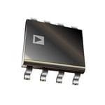
ICGOO电子元器件商城为您提供AD8350ARZ20-REEL7由Analog设计生产,在icgoo商城现货销售,并且可以通过原厂、代理商等渠道进行代购。 AD8350ARZ20-REEL7价格参考¥31.18-¥49.52。AnalogAD8350ARZ20-REEL7封装/规格:RF 放大器, 射频放大器 IC 手机 0Hz ~ 1GHz 8-SOIC。您可以下载AD8350ARZ20-REEL7参考资料、Datasheet数据手册功能说明书,资料中有AD8350ARZ20-REEL7 详细功能的应用电路图电压和使用方法及教程。
AD8350ARZ20-REEL7 是 Analog Devices Inc.(ADI)公司生产的一款高性能射频(RF)放大器,主要应用于需要高增益、低噪声和宽带宽的射频信号链中。

该器件是一款宽带、固定增益(20 dB)的电压反馈型放大器,具有优良的频率响应(带宽可达 1.8 GHz),适用于射频、中频(IF)和高速模拟信号处理领域。其典型应用场景包括:

1. 通信基础设施:如基站、无线接入系统、微波回传系统中的射频或中频放大,用于增强信号强度,提高接收灵敏度。

2. 测试与测量设备:在频谱分析仪、信号发生器等仪器中用于放大微弱信号,以保证测试精度和稳定性。

3. 工业控制系统:用于工业通信模块或传感器系统中,对高频模拟信号进行前置放大。

4. 医疗成像设备:如超声波设备中,作为高频信号放大器,提升图像质量和分辨率。

5. 雷达与安全系统:用于雷达接收机前端或安全监控系统中对射频信号进行放大处理。

AD8350ARZ20-REEL7采用 TSSOP 封装,适合表面贴装,适用于需要高稳定性和高性能的电子系统设计。其宽频带特性与高增益稳定性使其成为多种高频应用的理想选择。
| 参数 | 数值 |
| 产品目录 | |
| 描述 | IC AMP DIFF LOW-DISTORTION 8SOIC |
| 产品分类 | |
| 品牌 | Analog Devices Inc |
| 数据手册 | |
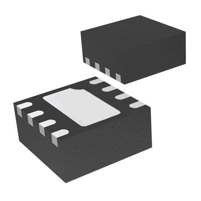
| 产品图片 |
|
| P1dB | -2.6dBm(0.5mW) |
| 产品型号 | AD8350ARZ20-REEL7 |
| RF类型 | 手机 |
| rohs | 无铅 / 符合限制有害物质指令(RoHS)规范要求 |
| 产品系列 | - |
| 产品培训模块 | http://www.digikey.cn/PTM/IndividualPTM.page?site=cn&lang=zhs&ptm=25165 |
| 产品目录页面 | |
| 供应商器件封装 | 8-SOIC |
| 其它名称 | AD8350ARZ20-REEL7CT |
| 包装 | 剪切带 (CT) |
| 噪声系数 | 5.9dB |
| 增益 | 20dB |
| 封装/外壳 | 8-SOIC(0.154",3.90mm 宽) |
| 标准包装 | 1 |
| 测试频率 | 250MHz |
| 电压-电源 | 5 V ~ 10 V |
| 电流-电源 | 28mA |
| 视频文件 | http://www.digikey.cn/classic/video.aspx?PlayerID=1364138032001&width=640&height=505&videoID=2245193150001 |
| 频率 | 0Hz ~ 1GHz |


- 商务部:美国ITC正式对集成电路等产品启动337调查
- 曝三星4nm工艺存在良率问题 高通将骁龙8 Gen1或转产台积电
- 太阳诱电将投资9.5亿元在常州建新厂生产MLCC 预计2023年完工
- 英特尔发布欧洲新工厂建设计划 深化IDM 2.0 战略
- 台积电先进制程称霸业界 有大客户加持明年业绩稳了
- 达到5530亿美元!SIA预计今年全球半导体销售额将创下新高
- 英特尔拟将自动驾驶子公司Mobileye上市 估值或超500亿美元
- 三星加码芯片和SET,合并消费电子和移动部门,撤换高东真等 CEO
- 三星电子宣布重大人事变动 还合并消费电子和移动部门
- 海关总署:前11个月进口集成电路产品价值2.52万亿元 增长14.8%


PDF Datasheet 数据手册内容提取
a Low Distortion 1.0 GHz Differential Amplifier AD8350 FEATURES FUNCTIONAL BLOCK DIAGRAM High Dynamic Range 8-Lead SOIC and (cid:3)SOIC Packages (with Enable) Output IP3: +28 dBm: Re 50 (cid:2) @ 250 MHz Low Noise Figure: 5.9dB @ 250 MHz Two Gain Versions: IN+ 1 8 IN– AD8350-15: 15 dB ENBL 2 + – 7 GND AD8350-20: 20 dB –3 dB Bandwidth: 1.0 GHz VCC 3 6 GND Single Supply Operation: 5 V to 10 V OUT+ 4 5 OUT– AD8350 Supply Current: 28 mA Input/Output Impedance: 200 (cid:2) Single-Ended or Differential Input Drive 8-Lead SOIC Package and 8-Lead microSOIC Package APPLICATIONS Cellular Base Stations Communications Receivers RF/IF Gain Block Differential A-to-D Driver SAW Filter Interface Single-Ended-to-Differential Conversion High Performance Video High Speed Data Transmission PRODUCT DESCRIPTION The amplifier can be operated down to 5 V with an OIP3 of The AD8350 series are high performance fully-differential +28dBm at 250 MHz and slightly reduced distortion perfor- amplifiers useful in RF and IF circuits up to 1000 MHz. The mance. The wide bandwidth, high dynamic range and temperature amplifier has excellent noise figure of 5.9 dB at 250 MHz. It stability make this product ideal for the various RF and IF offers a high output third order intercept (OIP3) of +28 dBm frequencies required in cellular, CATV, broadband, instrumen- at 250MHz. Gain versions of 15dB and 20 dB are offered. tation and other applications. The AD8350 is designed to meet the demanding performance The AD8350 is offered in an 8-lead single SOIC package and requirements of communications transceiver applications. It μSOIC package. It operates from 5V and 10V power supplies, enables a high dynamic range differential signal chain, with drawing 28mA typical. The AD8350 offers a power enable func- exceptional linearity and increased common-mode rejection. tion for power-sensitive applications. The AD8350 is fabricated The device can be used as a general purpose gain block, an using Analog Devices’ proprietary high speed complementary A-to-D driver, and high speed data interface driver, among bipolar process. The device is available in the industrial (–40°C to other functions. The AD8350 input can also be used as a single- +85°C) temperature range. ended-to-differential converter. Rev. C Document Feedback Information furnished by Analog Devices is believed to be accurate and reliable. However, no responsibility is assumed by Analog Devices for its use, nor for any infringements of patents or other One Technology Way, P.O. Box 9106, Norwood, MA 02062-9106, U.S.A. rights of third parties that may result from its use. Specifications subject to change without notice. No license is granted by implication or otherwise under any patent or patent rights of Analog Tel: 781.329.4700 ©2001–2016 Analog Devices, Inc. All rights reserved. Devices. Trademarks and registered trademarks are the property of their respective owners. Technical Support www.analog.com
AD8350–SPECIFICATIONS (@ 25(cid:4)C, V = 5 V, G = 15dB, unless otherwise noted. All specifications refer to S differential inputs and differential outputs unless noted.) Parameter Conditions Min Typ Max Unit DYNAMIC PERFORMANCE –3 dB Bandwidth V = 5 V, V = 1 V p-p 0.9 GHz S OUT V = 10 V, V = 1 V p-p 1.1 GHz S OUT Bandwidth for 0.1 dB Flatness V = 5 V, V = 1 V p-p 90 MHz S OUT V = 10 V, V = 1 V p-p 90 MHz S OUT Slew Rate V = 1 V p-p 2000 V/μs OUT Settling Time 0.1%, V = 1 V p-p 10 ns OUT Gain (S21)1 V = 5 V, f = 50 MHz 14 15 16 dB S Gain Supply Sensitivity V = 5 V to 10 V, f = 50 MHz 0.003 dB/V S Gain Temperature Sensitivity T to T –0.002 dB/°C MIN MAX Isolation (S12)1 f = 50 MHz –18 dB NOISE/HARMONIC PERFORMANCE 50 MHz Signal Second Harmonic V = 5 V, V = 1 V p-p –66 dBc S OUT V = 10 V, V = 1 V p-p –67 dBc S OUT Third Harmonic V = 5 V, V = 1 V p-p –65 dBc S OUT V = 10 V, V = 1 V p-p –70 dBc S OUT Output Second Order Intercept2 V = 5 V 58 dBm S V = 10 V 58 dBm S Output Third Order Intercept2 V = 5 V 28 dBm S V = 10 V 29 dBm S 250 MHz Signal Second Harmonic V = 5 V, V = 1 V p-p –48 dBc S OUT V = 10 V, V = 1 V p-p –49 dBc S OUT Third Harmonic V = 5 V, V = 1 V p-p –52 dBc S OUT V = 10 V, V = 1 V p-p –61 dBc S OUT Output Second Order Intercept2 V = 5 V 39 dBm S V = 10 V 40 dBm S Output Third Order Intercept2 V = 5 V 24 dBm S V = 10 V 28 dBm S 1 dB Compression Point (RTI)2 V = 5 V 2 dBm S V = 10 V 5 dBm S Voltage Noise (RTI) f = 150 MHz 1.7 nV/√Hz Noise Figure f = 150 MHz 6.8 dB INPUT/OUTPUT CHARACTERISTICS Differential Offset Voltage (RTI) V – V ±1 mV OUT+ OUT– Differential Offset Drift T to T 0.02 mV/°C MIN MAX Input Bias Current 15 μA Input Resistance Real 200 Ω CMRR f = 50 MHz –67 dB Output Resistance Real 200 Ω POWER SUPPLY Operating Range 4 11.0 V Quiescent Current Powered Up, V = 5 V 25 28 32 mA S Powered Down, V = 5 V 3 3.8 5.5 mA S Powered Up, V = 10 V 27 30 34 mA S Powered Down, V = 10 V 3 4 6.5 mA S Power-Up/Down Switching 15 ns Power Supply Rejection Ratio f = 50 MHz, V Δ = 1 V p-p –58 dB S OPERATING TEMPERATURE RANGE –40 +85 °C NOTES 1See Tables II–III for complete list of S-Parameters. 2Re: 50 Ω. Specifications subject to change without notice. –2– REV.C
AD8350 AD8350-20–SPECIFICATIONS (@ 25(cid:4)C, V = 5 V, G = 20dB, unless otherwise noted. All specifications refer to S differential inputs and differential outputs unless noted.) Parameter Conditions Min Typ Max Unit DYNAMIC PERFORMANCE –3 dB Bandwidth V = 5 V, V = 1 V p-p 0.7 GHz S OUT V = 10 V, V = 1 V p-p 0.9 GHz S OUT Bandwidth for 0.1 dB Flatness V = 5 V, V = 1 V p-p 90 MHz S OUT V = 10 V, V = 1 V p-p 90 MHz S OUT Slew Rate V = 1 V p-p 2000 V/μs OUT Settling Time 0.1%, V = 1 V p-p 15 ns OUT Gain (S21)1 V = 5 V, f = 50 MHz 19 20 21 dB S Gain Supply Sensitivity V = 5 V to 10 V, f = 50 MHz 0.003 dB/V S Gain Temperature Sensitivity T to T –0.002 dB/°C MIN MAX Isolation (S12)1 f = 50 MHz –22 dB NOISE/HARMONIC PERFORMANCE 50 MHz Signal Second Harmonic V = 5 V, V = 1 V p-p –65 dBc S OUT V = 10 V, V = 1 V p-p –66 dBc S OUT Third Harmonic V = 5 V, V = 1 V p-p –66 dBc S OUT V = 10 V, V = 1 V p-p –70 dBc S OUT Output Second Order Intercept2 V = 5 V 56 dBm S V = 10 V 56 dBm S Output Third Order Intercept2 V = 5 V 28 dBm S V = 10 V 29 dBm S 250 MHz Signal Second Harmonic V = 5 V, V = 1 V p-p –45 dBc S OUT V = 10 V, V = 1 V p-p –46 dBc S OUT Third Harmonic V = 5 V, V = 1 V p-p –55 dBc S OUT V = 10 V, V = 1 V p-p –60 dBc S OUT Output Second Order Intercept2 V = 5 V 37 dBm S V = 10 V 38 dBm S Output Third Order Intercept2 V = 5 V 24 dBm S V = 10 V 28 dBm S 1 dB Compression Point (RTI)2 V = 5 V –2.6 dBm S V = 10 V 1.8 dBm S Voltage Noise (RTI) f = 150 MHz 1.7 nV/√Hz Noise Figure f = 150 MHz 5.6 dB INPUT/OUTPUT CHARACTERISTICS Differential Offset Voltage (RTI) V – V ±1 mV OUT+ OUT– Differential Offset Drift T to T 0.02 mV/°C MIN MAX Input Bias Current 15 μA Input Resistance Real 200 Ω CMRR f = 50 MHz –52 dB Output Resistance Real 200 Ω POWER SUPPLY Operating Range 4 11.0 V Quiescent Current Powered Up, V = 5 V 25 28 32 mA S Powered Down, V = 5 V 3 3.8 5.5 mA S Powered Up, V = 10 V 27 30 34 mA S Powered Down, V = 10 V 3 4 6.5 mA S Power-Up/Down Switching 15 ns Power Supply Rejection Ratio f = 50 MHz, V Δ = 1 V p-p –45 dB S OPERATING TEMPERATURE RANGE –40 +85 °C NOTES 1See Tables II–III for complete list of S-Parameters. 2Re: 50 Ω. REV. C –3–
AD8350 ABSOLUTE MAXIMUM RATINGS* PIN FUNCTION DESCRIPTIONS Supply Voltage, V . . . . . . . . . . . . . . . . . . . . . . . . . . . . . 11 V S Pin Function Description Input Power Differential . . . . . . . . . . . . . . . . . . . . . . +8 dBm Internal Power Dissipation . . . . . . . . . . . . . . . . . . . . 400 mW 1, 8 IN+, IN– Differential Inputs. IN+ and IN– θJASOIC (R) . . . . . . . . . . . . . . . . . . . . . . . . . . . . . . . 100°C/W should be ac-coupled (pins have a dc θJAμSOIC (RM) . . . . . . . . . . . . . . . . . . . . . . . . . . . . 133°C/W bias of midsupply). Differential input Maximum Junction Temperature . . . . . . . . . . . . . . . . . 125°C impedance is 200Ω. Operating Temperature Range . . . . . . . . . . . –40°C to +85°C 2 ENBL Power-up Pin. A high level (5 V) enables Storage Temperature Range . . . . . . . . . . . . –65°C to +150°C the device; a low level (0 V) puts device Lead Temperature Range (Soldering 60 sec) . . . . . . . . . 300°C in sleep mode. *Stresses above those listed under Absolute Maximum Ratings may cause perma- 3 V Positive Supply Voltage. 5 V to 10V. CC nent damage to the device. This is a stress rating only; functional operation of the 4, 5 OUT+, OUT– Differential Outputs. OUT+ and device at these or any other conditions above those indicated in the operational section of this specification is not implied. Exposure to absolute maximum rating OUT– should be ac-coupled (pins have conditions for extended periods may affect device reliability. a dc bias of midsupply). Differential input impedance is 200Ω. PIN CONFIGURATION 6, 7 GND Common External Ground Reference. IN+ 1 8 IN– ENBL 2 AD8350 7 GND TOP VIEW VCC 3 (Not to Scale) 6 GND OUT+ 4 5 OUT– CAUTION ESD (electrostatic discharge) sensitive device. Electrostatic charges as high as 4000 V readily WARNING! accumulate on the human body and test equipment and can discharge without detection. Although the AD8350 features proprietary ESD protection circuitry, permanent damage may occur on devices subjected to high-energy electrostatic discharges. Therefore, proper ESD precautions are recommended to avoid performance degradation or loss of functionality. ESD SENSITIVE DEVICE –4– REV. C
Typical Performance Characteristics–AD8350 50 20 25 VCC = 10V 40 mA VCC = 10V 15 VCC = 10V 20 – T EN 30 dB dB VCC = 5V CURR VCC = 5V AIN – 10 AIN – 15 Y 20 G G L P P SU 5 10 10 VCC = 5V 0 0 5 –40 –20 0 20 40 60 80 1 10 100 1k 10k 1 10 100 1k 10k TEMPERATURE – (cid:4)C FREQUENCY – MHz FREQUENCY – MHz TPC 1.Supply Current vs. TPC 2.AD8350-15 Gain (S21) vs. TPC 3.AD8350-20 Gain (S21) vs. Temperature Frequency Frequency 350 350 500 300 300 400 (cid:2)SOIC (cid:2) (cid:2) (cid:2) CE – 250 VCC = 10V CE – 250 VCC = 10V CE – 300 SOIC N N N A A A D D D PE200 PE200 PE 200 IM VCC = 5V IM IM 150 150 VCC = 5V 100 100 100 0 1 10 100 1k 1 10 100 1k 0 10 100 1000 FREQUENCY – MHz FREQUENCY – MHz FREQUENCY – MHz TPC 4.AD8350-15 Input Imped- TPC 5.AD8350-20 Input Impedance TPC 6.AD8350-15 Output Impedance ance vs. Frequency vs. Frequency vs. Frequency 800 –5 –10 (cid:3)SOIC 600 –10 –15 (cid:2) B B CE – N – d N – d VCC = 10V DAN 400 SOIC ATIO–15 VCC = 10V ATIO–20 E L L P O O M S S I I I 200 –20 VCC = 5V –25 VCC = 5V 0 –25 –30 0 10 100 1000 1 10 100 1k 10k 1 10 100 1k 10k FREQUENCY – MHz FREQUENCY – MHz FREQUENCY – MHz TPC 7.AD8350-20 Output Imped- TPC 8.AD8350-15 Isolation (S12) TPC 9.AD8350-20 Isolation (S12) ance vs. Frequency vs. Frequency vs. Frequency REV. C –5–
AD8350 –40 –40 –45 VOUT = 1V p-p VOUT = 1V p-p FO = 50MHz –45 HD2 (VCC = 10V) –45 HD2 (VCC = 5V) HD3 (VCC = 5V) –50 HD2 (VCC = 5V) –50 –55 HD2 (VCC = 5V) ORTION – dBc––5650 HD3 (VCC = 5V) ORTION – dBc––5650 HD2 (VCC = 10V) ORTION – dBc–65 HD2 (VCC = 10V) DIST–65 HD3 (VCC = 10V) DIST–65 HD3 (VCC = 5V) DIST –70 –70 HD3 (VCC = 10V) –75 HD3 (VCC = 10V) –75 –75 –80 –80 –85 0 50 100 150 200 250 300 0 50 100 150 200 250 300 0 0.5 1 1.5 2 2.5 3 3.5 FUNDAMENTAL FREQUENCY – MHz FUNDAMENTAL FREQUENCY – MHz OUTPUT VOLTAGE – V p-p TPC 10.AD8350-15 Harmonic TPC 11.AD8350-20 Harmonic Dis- TPC 12.AD8350-15 Harmonic Distor- Distortion vs. Frequency tortion vs. Frequency tion vs. Differential Output Voltage –45 66 66 FO = 50MHz HD2 (VCC = 5V) HD3 (VCC = 5V) 61 61 Bc–55 (cid:2)0) 56 VCC = 10V (cid:2)0) 56 VCC = 10V N – d Re: 5 Re: 5 DISTORTIO–65 HD3 (VCC =H 1D02V )(VCC = 10V) OIP2 – dBm ( 5416 VCC = 5V OIP2 – dBm ( 5416 VCC = 5V –75 41 41 –85 36 36 0 0.5 1 1.5 2 2.5 3 3.5 0 50 100 150 200 250 300 0 50 100 150 200 250 300 OUTPUT VOLTAGE – V p-p FREQUENCY – MHz FREQUENCY – MHz TPC 13.AD8350-20 Harmonic Distor- TPC 14.AD8350-15 Output Referred TPC 15.AD8350-20 Output Referred tion vs. Differential Output Voltage IP2 vs. Frequency IP2 vs. Frequency 41 41 10.0 INPUT REFERRED (cid:2)) 36 36 e: 50 7.5 VCC = 10V (cid:2)Re: 50) 31 VCC = 10V (cid:2)Re: 50) 31 VCC = 10V – dBm (R 5.0 m ( 26 m ( 26 ON 2.5 OIP3 – dB 21 VCC = 5V OIP3 – dB 21 VCC = 5V MPRESSI 0 VCC = 5V O C 16 16 B –2.5 d 1 11 11 –5.0 0 50 100 150 200 250 300 0 50 100 150 200 250 300 0 100 200 300 400 500 600 FREQUENCY – MHz FREQUENCY – MHz FREQUENCY – MHz TPC 16.AD8350-15 Output Referred TPC 17.AD8350-20 Output Referred TPC 18.AD8350-15 1 dB Compres- IP3 vs. Frequency IP3 vs. Frequency sion vs. Frequency –6– REV. C
AD8350 7.5 10 10 INPUT REFERRED (cid:2)) e: 50 5.0 9 9 R dBm ( 2.5 VCC = 10V E – dB 8 E – dB 8 SSION – 0 E FIGUR 7 VCC = 10V E FIGUR 7 VCC = 10V E S S MPR–2.5 NOI VCC = 5V NOI B CO–5.0 VCC = 5V 6 6 VCC = 5V d 1 –7.5 5 5 0 100 200 300 400 500 600 0 50 100150200250300350400450500 0 50 100150200250300350400450500 FREQUENCY – MHz FREQUENCY – MHz FREQUENCY – MHz TPC 19.AD8350-20 1 dB Compres- TPC 20.AD8350-15 Noise Figure TPC 21.AD8350-20 Noise Figure sion vs. Frequency vs. Frequency vs. Frequency 25 100 –20 AD8350-20 VCC = 5V 20 50 VOUT + (VCC = 5V) –30 15 V m 0 –40 10 AD8350-15 – GAIN – dB 50 UT OFFSET –1–0500 VOUT – (VVOCUCT =+ 5(VVC)C = 10V) PSRR – dB––5600 AD8350-20 –5 TP OU–150 –70 AD8350-15 –10 –200 VOUT – (VCC = 10V) –80 –15 –20 –250 –90 1 2 3 4 5 6 7 8 9 10 –40 –20 0 20 40 60 80 1 10 100 1k VCC – Volts TEMPERATURE – (cid:4)C FREQUENCY – MHz TPC 22.AD8350 Gain (S21) vs. TPC 23.AD8350 Output Offset Volt- TPC 24.AD8350 PSRR vs. Frequency Supply Voltage age vs. Temperature –20 VCC = 5V 500mV VCC = 5V –30 AD8350-20 VOUT –40 B – d–50 R R S–60 AD8350-15 P –70 ENBL –80 5V 30ns –90 1 10 100 1k FREQUENCY – MHz TPC 25.AD8350 CMRR vs. Frequency TPC 26.AD8350 Power-Up/Down Response Time REV. C –7–
AD8350 APPLICATIONS LS/2 CAC CAC LS/2 Using the AD8350 Figure 1 shows the basic connections for operating the AD8350. 8 7 6 5 A single supply in the range 5 V to 10 V is required. The power RS/2 AD8350 supply pin should be decoupled using a 0.1μF capacitor. The ENBL pin is tied to the positive supply or to 5V (when VCC = VS CP – CP RLOAD + 10 V) for normal operation and should be pulled to ground to put the device in sleep mode. Both the inputs and the outputs RS/2 have dc bias levels at midsupply and should be ac-coupled. 1 2 3 4 Also shown in Figure 1 are the impedance balancing requirements, LS/2 CAC CAC LS/2 either resistive or reactive, of the input and output. With an 0.1(cid:3)F input and output impedance of 200Ω, the AD8350 should be ENBL (5V) driven by a 200Ω source and loaded by a 200Ω impedance. A +VS (5V TO 10V) reactive match can also be implemented. Figure 3.Reactively Matching the Input and Output C2 C4 SOURCE 0.001(cid:3)F 0.001(cid:3)F LOAD Z = 100(cid:2) LS CAC CAC LS 8 7 6 5 AD8350 8 7 6 5 RS – AD8350 Z = 200(cid:2) + VS CP – CP RLOAD + 1 2 3 4 Z = 100(cid:2) 1 2 3 4 C1 C3 0.001(cid:3)F 0.001(cid:3)F C0.51(cid:3)F CAC CAC ENBL (5V) 0.1(cid:3)F +VS (5V TO 10V) ENBL (5V) Figure 1.Basic Connections for Differential Drive +VS (5V TO 10V) Figure 4.Single-Ended Equivalent Circuit Figure 2 shows how the AD8350 can be driven by a single- ended source. The unused input should be ac-coupled to ground. When the source impedance is smaller than the load impedance, When driven single-endedly, there will be a slight imbalance in a step-up matching network is required. A typical step-up network the differential output voltages. This will cause an increase in is shown on the input of the AD8350 in Figure 3. For purely the second order harmonic distortion (at 50MHz, with V = resistive source and load impedances the resonant approach may CC 10 V and V = 1 V p-p, –59 dBc was measured for the second be used. The input and output impedance of the AD8350 can be OUT harmonic on AD8350-15). modeled as a real 200 Ω resistance for operating frequencies less than 100 MHz. For signal frequencies exceeding 100 MHz, classi- LOAD cal Smith Chart matching techniques should be invoked in order to deal with the complex impedance relationships. Detailed S 0.0C012(cid:3)F 8 7 6 5 0.0C014(cid:3)F parameter data measured differentially in a 200 Ω system can be AD8350 found in Tables II and III. – Z = 200(cid:2) For the input matching network the source resistance is less + than the input resistance of the AD8350. The AD8350 has a nominal 200 Ω input resistance from Pins 1 to 8. The reactance 1 2 3 4 of the ac-coupling capacitors, CAC, should be negligible if 100 nF SOURCE capacitors are used and the lowest signal frequency is greater Z = 200(cid:2) C1 C3 than 1 MHz. If the series reactance of the matching network 0.001(cid:3)F C5 0.001(cid:3)F inductor is defined to be XS = 2 π f LS, and the shunt reactance ENBL (5V) 0.1(cid:3)F of the matching capacitor to be X = (2 π f C )–1, then: P P +VS (5V TO 10V) R ×R R Figure 2.Basic Connections for Single-Ended Drive XS = S X LOAD whereXP =RLOAD × R S–R (1) P LOAD S Reactive Matching In practical applications, the AD8350 will most likely be matched For a 70 MHz application with a 50 Ω source resistance, and using reactive matching components as shown in Figure 3. assuming the input impedance is 200 Ω, or RLOAD = RIN = 200 Ω, Matching components can be calculated using a Smith Chart or then XP = 115.5 Ω and XS = 86.6 Ω, which results in the follow- by using a resonant approach to determine the matching network ing component values: that results in a complex conjugate match. In either situation, C = (2 π × 70 × 106 × 115.5)–1 = 19.7 pF and P the circuit can be analyzed as a single-ended equivalent circuit to ease calculations as shown in Figure 4. L = 86.6 × (2 π × 70 × 106)–1 = 197 nH S –8– REV. C
AD8350 For the output matching network, if the output source resis- The same results could be found using a Smith Chart as shown tance of the AD8350 is greater than the terminating load in Figure 7. In this example, a shunt capacitor and a series inductor resistance, a step-down network should be employed as shown are used to match the 200 Ω source to a 50 Ω load. For a fre- on the output of Figure 3. For a step-down matching network, quency of 10 MHz, the same capacitor and inductor values the series and parallel reactances are calculated as: previously found using the resonant approach will transform the 200 Ω source to match the 50 Ω load. At frequencies exceeding R ×R R 100 MHz, the S parameters from Tables II and III should be X = S LOAD whereX =R × LOAD (2) S X P S R –R used to account for the complex impedance relationships. P S LOAD For a 10 MHz application with the 200 Ω output source resistance of the AD8350, R = 200 Ω, and a 50 Ω load termination, R = S LOAD 50 Ω, then X = 115.5 Ω and X = 86.6 Ω, which results in P S the following component values: C = (2 π × 10 × 106 × 115.5)–1 = 138 pF and P L = 86.6 × (2 π × 10 × 106)–1 = 1.38 μH S The same results can be obtained using the plots in Figure 5 LOAD SOURCE and Figure 6. Figure 5 shows the normalized shunt reactance versus the normalized source resistance for a step-up matching SHUNT C network, R < R . By inspection, the appropriate reactance S LOAD SERIES L can be found for a given value of R /R . The series reactance S LOAD is then calculated using X = R R /X The same technique S S LOAD P. can be used to design the step-down matching network using Figure 6. 2 Figure 7.Smith Chart Representation of Step-Down Network /RPLOAD11..86 RSOURCE XS XP RLOAD Aeqftueirv adleentetr cmiricnuinitg, tthhee mmaattcchhiningg e nleemtwenotrsk nfeoerd t htoe bsien agplep-leiendd eind a E – X1.4 differential manner. The series reactance needs to be split such NC1.2 that the final network is balanced. In the previous examples, this A CT 1 simply translates to splitting the series inductor into two equal A E halves as shown in Figure 3. D R0.8 ALIZE0.6 GThaein e Affedcjtuisvtem geanint of the AD8350 can be reduced using a num- M R0.4 ber of techniques. Obviously a matched attenuator network will O N0.2 reduce the effective gain, but this requires the addition of a separate component which can be prohibitive in size and cost. 0 1 5 937 1 5 937 1 5 937 1 5 937 The attenuator will also increase the effective noise figure resulting 0 0 011 2 2 233 4 4 455 6 6 677 0. 0. 0.0.0. 0. 0. 0.0.0. 0. 0. 0.0.0. 0. 0. 0.0.0. in an SNR degradation. A simple voltage divider can be imple- NORMALIZED SOURCE RESISTANCE – RSOURCE/RLOAD mented using the combination of the driving impedance of the Figure 5.Normalized Step-Up Matching Components previous stage and a shunt resistor across the inputs of the AD8350 as shown in Figure 8. This provides a compact solution but suffers from an increased noise spectral density at the input 3.2 of the AD8350 due to the thermal noise contribution of the RSOURCE RLOAD 3 XP XS RLOAD sthhruonutg rhe stihseto ur.s eT ohfe f ienepdubta cimk preesdisatnocres caas ns hboew dny nina mFiigcaulrley 9al.t Terheids X/P will result in a similar attenuation of the input signal by virtue E – 2.8 of the voltage divider established from the driving source imped- C N ance and the reduced input impedance of the AD8350. Yet A CT2.6 this technique does not significantly degrade the SNR with A RE the unnecessary increase in thermal noise that arises from a truly D E2.4 resistive attenuator network. Z LI A M OR2.2 N 2 2 4 8 2 6 4 4 8 2 6 6 4 8 2 6 8 4 8 2. 2. 3. 3. 4. 4. 5. 5. 6. 6. 7. 7. 8. 8. NORMALIZED SOURCE RESISTANCE – RSOURCE/RLOAD Figure 6.Normalized Step-Down Matching Components REV. C –9–
AD8350 CAC CAC The insertion loss and the resultant power gain for multiple shunt resistor values is summarized in Table I. The source 8 7 6 5 resistance and input impedance need careful attention when RS RSHUNT AD8350 RL using Equation 1. The reactance of the input impedance of the AD8350 and the ac-coupling capacitors need to be considered – VS before assuming they have negligible contribution. Figure 10 + shows the effective power gain for multiple values of R for SHUNT RS RSHUNT RL the AD8350-15 and AD8350-20. 1 2 3 4 Table I. Gain Adjustment Using Shunt Resistor, CAC CAC R = 100 (cid:2) and R = 100 (cid:2) Single-Ended S IN 0.1(cid:3)F ENBL (5V) Power Gain–dB +VS (5V TO 10V) RSHUNT–(cid:2) IL–dB AD8350-15 AD8350-20 Figure 8.Gain Reduction Using Shunt Resistor 50 6.02 8.98 13.98 100 3.52 11.48 16.48 200 1.94 13.06 18.06 RFEXT 300 1.34 13.66 18.66 400 1.02 13.98 18.98 CAC CAC RS 8 7 6 5 RL 20 AD8350 18 – VS 16 AD8350-20 + 14 RS RL 1 2 3 4 B 12 d AD8350-15 CAC ENBL 0.1(cid:3)F CAC GAIN – 108 (5V) +VS 6 (5V TO 10V) 4 RFEXT 2 Figure 9.Dynamic Gain Reduction 0 0 100 200 300 400 500 600 700 800 RSHUNT – (cid:2) Figure 8 shows a typical implementation of the shunt divider Figure 10.Gain for Multiple Values of Shunt Resistance concept. The reduced input impedance that results from the for Circuit in Figure 8 parallel combination of the shunt resistor and the input impedance The gain can be adjusted dynamically by employing external of the AD8350 adds attenuation to the input signal effectively feedback resistors as shown in Figure 9. The effective attenua- reducing the gain. For frequencies less than 100 MHz, the input impedance of the AD8350 can be modeled as a real 200 Ω resis- tion is a result of the lowered input impedance as with the shunt resistor method, yet there is no additional noise contribution at tance (differential). Assuming the frequency is low enough to the input of the device. It is necessary to use well-matched resistors ignore the shunt reactance of the input, and high enough such to minimize common-mode offset errors. Quality 1% tolerance that the reactance of moderately sized ac-coupling capacitors resistors should be used along with a symmetric board layout to can be considered negligible, the insertion loss, IL, due to the help guarantee balanced performance. The effective gain for mul- shunt divider can be expressed as: tiple values of external feedback resistors is shown in Figure 11. ⎡ R ⎤ ⎢ IN ⎥ IL(dB)=20×Log ⎢ (RIN +RS) ⎥ 10⎢ R (cid:2)R ⎥ IN SHUNT ⎣⎢(R (cid:2)R +R )⎦⎥ IN SHUNT S where (3) R ×R R (cid:2)R = IN SHUNT andR =100Ωsingle−ended IN SHUNT R +R IN IN SHUNT –10– REV. C
AD8350 20 Driving Lighter Loads It is not necessary to load the output of the AD8350 with a 18 AD8350-20 200 Ω differential load. Often it is desirable to try to achieve a 16 complex conjugate match between the source and load in order 14 to minimize reflections and conserve power. But if the AD8350 is driving a voltage responding device, such as an ADC, it is no B 12 AIN – d 10 AD8350-15 ldoinstgoerrt inonec pesesraforyrm toa nmcea xwimilli zaec tpuoawlleyr itmrapnrsofveer .w Thheen hdarrimvinognic G 8 loads greater than 200 Ω. The lighter load requires less cur- 6 rent driving capability on the output stages of the AD8350 resulting in improved linearity. Figure 12 shows the improve- 4 ment in second and third harmonic distortion for increasing 2 differential load resistance. 0 0 500 1000 1500 2000 –66 RFEXT – (cid:2) Figure 11.Power Gain vs. External Feedback Resistors –68 for the AD8350-15 and AD8350-20 with R = 100 Ω and S R = 100 Ω –70 L c HD3 B The power gain of any two-port network is dependent on the d –72 – source and load impedance. The effective gain will change if the N differential source and load impedance is not 200 Ω. The single- TIO –74 R ended input and output resistance of the AD8350 can be modeled STO –76 using the following equations: DI –78 R +R HD2 R = F L –80 IN ⎛R +R ⎞ ⎜ F L⎟ +1+g ×R (4) ⎝ R ⎠ m L –82 INT 200 300 400 500 600 700 800 900 1000 RLOAD – (cid:2) and Figure 12.Second and Third Harmonic Distortion vs. Differential Load Resistance for the AD8350-15 with R + 1 VS = 5 V, f = 70 MHz, and VOUT = 1 V p-p F 1 1 + R R R +R R = S INT ≈ F S for R ≤1kΩ OUT ⎛ ⎞ 1+g ×R S m S ⎜ 1 ⎟ (5) 1+g ×⎜ ⎟ m ⎜ 1 + 1 ⎟ ⎝ R R ⎠ S INT where R = R //R F FEXT FINT R = R Feedback External FEXT R = 662 Ω for the AD8350-15 FINT = 1100 Ω for the AD8350-20 R = 25000 Ω INT g = 0.066 mhos for the AD8350-15 m = 0.110 mhos for the AD8350-20 R = R Source (Single-Ended) S R = R Load (Single-Ended) L R = R Input (Single-Ended) IN R = R Output (Single-Ended) OUT The resultant single-ended gain can be calculated using the following equation: ( ) R × g ×R −1 GV = R +RL+Rm+RF×R ×g (6) L S F L S m REV. C –11–
AD8350 Table II. Typical Scattering Parameters for the AD8350-15: V = 5 V, Differential Input and Output, Z (diff) = 200 (cid:2), CC SOURCE Z (diff) = 200 (cid:2) LOAD Frequency – MHz S11 S12 S21 S22 25 0.015∠–48.8° 0.119∠176.3° 5.60∠–4.3° 0.034∠–4.8° 50 0.028∠–65.7° 0.119∠171.1° 5.61∠–8.9° 0.032∠–14.3° 75 0.043∠–75.3° 0.119∠166.9° 5.61∠–13.5° 0.036∠–30.2° 100 0.057∠–87.5° 0.120∠163.5° 5.61∠–17.9° 0.043∠–39.6° 125 0.073∠–91.8° 0.119∠159.8° 5.65∠–22.6° 0.053∠–40.6° 150 0.080∠–95.6° 0.120∠154.8° 5.68∠–27.0° 0.058∠–37° 175 0.100∠–97.4° 0.117∠151.2° 5.73∠–31.8° 0.072∠–45.1° 200 0.111∠–99.1° 0.121∠147.3° 5.78∠–36.3° 0.077∠–47.7° 225 0.128∠–103.2° 0.120∠143.7° 5.83∠–41.0° 0.091∠–52.5° 250 0.141∠–106.7° 0.120∠140.3° 5.90∠–45.6° 0.104∠–55.1° 275 0.151∠–109.7° 0.120∠136.6° 6.02∠–50.2° 0.108∠–54.2° 300 0.161∠–111.9° 0.123∠132.9° 6.14∠–55.1° 0.122∠–51.5° 325 0.179∠–114.7° 0.121∠130.7° 6.19∠–60.2° 0.135∠–55.6° 350 0.187∠–117.4° 0.122∠126.6° 6.27∠–65.0° 0.150∠–56.9° 375 0.194∠–121° 0.123∠123.6° 6.43∠–70.1° 0.162∠–60.9° 400 0.199∠–121.2° 0.124∠120.1° 6.61∠–75.8° 0.187∠–60.3° 425 0.215∠–122.6° 0.126∠117.2° 6.77∠–81.7° 0.215∠–63.3° 450 0.225∠–127.0° 0.126∠113.9° 6.91∠–87.6° 0.242∠–63.9° 475 0.225∠–127.7° 0.126∠112° 7.06∠–93.8° 0.268∠–65.2° 500 0.244∠–129.9° 0.128∠108.1° 7.27∠–99.8° 0.304∠–68.2° Table III. Typical Scattering Parameters for the AD8350-20: V = 5 V, Differential Input and Output, Z (diff) = 200 (cid:2), CC SOURCE Z (diff) = 200 (cid:2) LOAD Frequency – MHz S11 S12 S21 S22 25 0.017∠–142.9° 0.074∠174.9° 9.96∠–4.27° 0.023–16.6° 50 0.033∠–114.9° 0.074∠171.0° 9.98∠–8.9° 0.022∠–2.7° 75 0.055∠–110.6° 0.075∠167.0° 9.98∠–13.3° 0.023∠–23.5° 100 0.073∠–109.4° 0.075∠163.1° 10.00∠–17.7° 0.029∠–22.7° 125 0.089∠–112.1° 0.075∠159.2° 10.12∠–22.1° 0.037∠–18.0° 150 0.098∠–116.5° 0.076∠153.8° 10.20∠–26.4° 0.045∠–3.2° 175 0.124∠–118.1° 0.075∠150.2° 10.34∠–30.9° 0.055∠–15.7° 200 0.141∠–119.4° 0.076∠147.2° 10.50∠–35.6° 0.065∠–15.6° 225 0.159∠–122.6° 0.077∠142.2° 10.65∠–40.1° 0.080∠–17.7° 250 0.170∠–128.5° 0.078∠139.5° 10.80∠–44.7° 0.085∠–22.4° 275 0.186∠–131.6° 0.078∠135.8° 11.14∠–49.3° 0.096∠–23.5° 300 0.203∠–132.9° 0.080∠132.5° 11.45∠–54.7° 0.116∠–25.9° 325 0.215∠–135.0° 0.080∠129.3° 11.70∠–60.3° 0.139∠–29.6° 350 0.222∠–136.9° 0.082∠125.9° 11.93∠–65.0° 0.161∠–32.2° 375 0.242∠–142.4° 0.082∠123.6° 12.39∠–70.3° 0.173∠–38.6° 400 0.240∠–145.2° 0.084∠120.3° 12.99∠–76.8° 0.207∠–37.6° 425 0.267∠–146.7° 0.084∠117.3° 13.34∠–84.0° 0.241∠–48.1° 450 0.266∠–150.7° 0.086∠115.1° 13.76∠–90.1° 0.265∠–49.7° 475 0.267∠–153.7° 0.087∠112.8° 14.34∠–97.5° 0.317∠–53.5° 500 0.285∠–161.1° 0.088∠110.9° 14.89∠–105.0° 0.359∠–59.2° REV. C –12–
AD8350 OUTLINE DIMENSIONS 5.00(0.1968) 4.80(0.1890) 8 5 4.00(0.1574) 6.20(0.2441) 3.80(0.1497) 1 4 5.80(0.2284) 1.27(0.0500) 0.50(0.0196) BSC 1.75(0.0688) 0.25(0.0099) 45° 0.25(0.0098) 1.35(0.0532) 8° 0.10(0.0040) 0° COPLANARITY 0.51(0.0201) 0.10 SEATING 0.31(0.0122) 0.25(0.0098) 10..2470((00..00510507)) PLANE 0.17(0.0067) COMPLIANTTOJEDECSTANDARDSMS-012-AA C(RINOEFNPEATRRREOENNLCLTEIHNEOGSNDELISYM)AEANNRDSEIAORRNOESUNANORDETEDAIN-POMPFRIFLOLMPIMIRLELIATIMTEEERTFSEO;RIRNECUQHSUEDIVIINMAELDENENSSTIIOGSNNFS.OR 012407-A Figure 14. 8-Lead Standard Small Outline Package [SOIC_N] Narrow Body (R-8) Dimensions shown in millimeters and (inches) 3.20 3.00 2.80 8 5 5.15 3.20 4.90 3.00 4.65 2.80 1 4 PIN 1 IDENTIFIER 0.65 BSC 0.95 15° MAX 0.85 1.10 MAX 0.75 0.80 0.15 0.40 6° 0.23 0.55 CO0P.0L50A.1N0ARICTOYMPLIANT0. 2T5O JEDEC STA0°NDARDS 0M.0O9-187-AA 0.40 10-07-2009-B Figure 15. 8-Lead Mini Small Outline Package [MSOP] (RM-8) Dimensions shown in millimeters Rev. C | Page 13
AD8350 ORDERING GUIDE Model1 Temperature Range Package Description Package Option Branding AD8350ARZ15-REEL7 −40°C to +85°C 8-Lead SOIC_N R-8 AD8350ARMZ15 −40°C to +85°C 8-Lead MSOP RM-8 Q0T AD8350ARMZ15-REEL7 −40°C to +85°C 8-Lead MSOP RM-8 Q0T AD8350ARMZ20 −40°C to +85°C 8-Lead MSOP RM-8 J2P AD8350ARMZ20-REEL7 −40°C to +85°C 8-Lead MSOP RM-8 J2P AD8350ARM20-REEL7 −40°C to +85°C 8-Lead MSOP RM-8 J2P AD8350ARZ20-REEL7 −40°C to +85°C 8-Lead SOIC_N R-8 1 Z = RoHS Compliant Part. REVISION HISTORY 11/2016—Rev. B to Rev. C Changes to Ordering Guide .......................................................... 14 5/2013—Rev. A to Rev. B Deleted Evaluation Board Section ................................................ 12 Updated Outline Dimensions ....................................................... 13 Changes to Ordering Guide .......................................................... 14 6/2001—Rev. 0 to Rev. A ©2001-2016 Analog Devices, Inc. All rights reserved. Trademarks and registered trademarks are the property of their respective owners. D01014-0-11/16(C) Rev. C | Page 14
Mouser Electronics Authorized Distributor Click to View Pricing, Inventory, Delivery & Lifecycle Information: A nalog Devices Inc.: AD8350ARMZ15 AD8350ARMZ20 AD8350ARMZ15-REEL7 AD8350ARMZ20-REEL7 AD8350ARZ15-REEL7 AD8350ARZ20-REEL7