ICGOO在线商城 > 射频/IF 和 RFID > RF 放大器 > HMC604LP3ETR
 Datasheet下载
- 型号: HMC604LP3ETR
- 制造商: Hittite
- 库位|库存: xxxx|xxxx
- 要求:
| 数量阶梯 | 香港交货 | 国内含税 |
| +xxxx | $xxxx | ¥xxxx |
查看当月历史价格
查看今年历史价格
HMC604LP3ETR产品简介:
ICGOO电子元器件商城为您提供HMC604LP3ETR由Hittite设计生产,在icgoo商城现货销售,并且可以通过原厂、代理商等渠道进行代购。 HMC604LP3ETR价格参考¥5.62-¥6.13。HittiteHMC604LP3ETR封装/规格:RF 放大器, RF Amplifier IC General Purpose 4.8GHz ~ 6GHz 16-QFN (3x3)。您可以下载HMC604LP3ETR参考资料、Datasheet数据手册功能说明书,资料中有HMC604LP3ETR 详细功能的应用电路图电压和使用方法及教程。
HMC604LP3ETR是Analog Devices Inc.(亚德诺半导体)推出的一款高性能RF放大器,属于宽频带、高线性度的增益放大器。该器件主要工作在20 MHz至6 GHz的频率范围内,适用于多种射频和微波应用场景。

其典型应用场景包括:无线通信基础设施,如蜂窝基站中的收发模块,用于增强信号覆盖和传输质量;宽带通信系统,如点对点微波链路、卫星通信终端等,因其宽频带特性可支持多频段操作;国防与电子战系统,如雷达前端、信号侦察和干扰设备,得益于其高线性度和低噪声性能;此外,也广泛用于测试与测量仪器,如频谱分析仪、信号发生器等,以提升射频信号处理精度。

HMC604LP3ETR采用紧凑的3 mm × 3 mm陶瓷封装(SMT工艺),具有良好的温度稳定性和可靠性,适合在严苛环境下运行。其内部集成匹配网络,简化了电路设计,降低了外围元件需求,有助于缩短产品开发周期。

综上,HMC604LP3ETR凭借其宽频带、高增益、优异的线性度和稳定性,广泛应用于通信、军工和高端仪器领域,是一款适用于高频、高性能要求系统的理想RF放大器。
| 参数 | 数值 |
| 产品目录 | |
| 描述 | IC MMIC AMP LNA BYPASS 16-QFN |
| 产品分类 | |
| 品牌 | Hittite Microwave Corporation |
| 数据手册 | |
| 产品图片 |
|
| P1dB | 14dBm |
| 产品型号 | HMC604LP3ETR |
| RF类型 | 通用 |
| rohs | 无铅 / 符合限制有害物质指令(RoHS)规范要求 |
| 产品系列 | - |
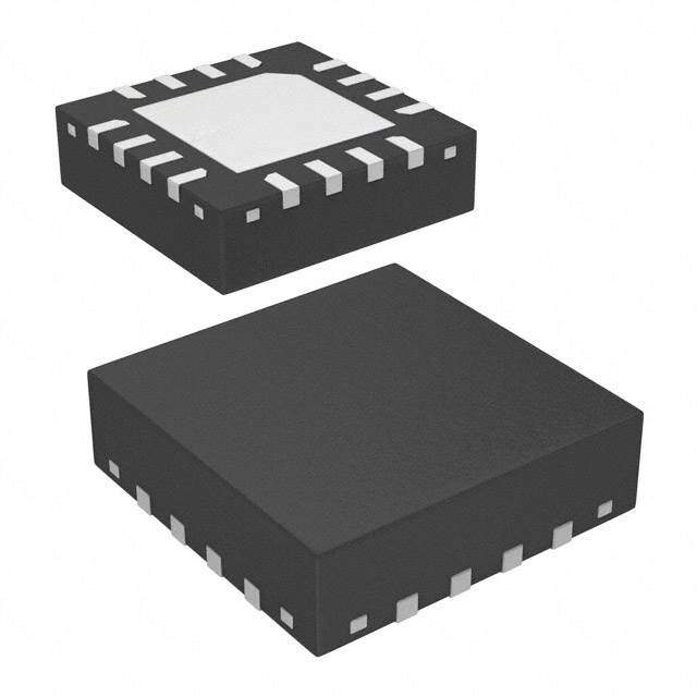
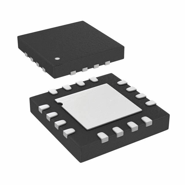
| 供应商器件封装 | 16-QFN(3x3) |
| 其它名称 | 1127-1479-2 |
| 包装 | 带卷 (TR) |
| 噪声系数 | 1.5dB |
| 增益 | 15dB |
| 封装/外壳 | 16-VQFN 裸露焊盘 |
| 标准包装 | 500 |
| 测试频率 | - |
| 电压-电源 | 2.7 V ~ 5.5 V |
| 电流-电源 | 42mA |
| 频率 | 4.8GHz ~ 6GHz |


- 商务部:美国ITC正式对集成电路等产品启动337调查
- 曝三星4nm工艺存在良率问题 高通将骁龙8 Gen1或转产台积电
- 太阳诱电将投资9.5亿元在常州建新厂生产MLCC 预计2023年完工
- 英特尔发布欧洲新工厂建设计划 深化IDM 2.0 战略
- 台积电先进制程称霸业界 有大客户加持明年业绩稳了
- 达到5530亿美元!SIA预计今年全球半导体销售额将创下新高
- 英特尔拟将自动驾驶子公司Mobileye上市 估值或超500亿美元
- 三星加码芯片和SET,合并消费电子和移动部门,撤换高东真等 CEO
- 三星电子宣布重大人事变动 还合并消费电子和移动部门
- 海关总署:前11个月进口集成电路产品价值2.52万亿元 增长14.8%


PDF Datasheet 数据手册内容提取
HMC604LP3 / 604LP3E v00.0308 GaAs PHEMT MMIC LOW NOISE AMPLIFIER w/ BYPASS MODE, 4.8 - 6.0 GHz 7 Typical Applications Features The HmC604lp3 / HmC604lp3e is ideal for: Noise figure: 1.5 dB T m • wimAX/C-band radio output ip3: +26 dBm s • fixed wireless Gain: 15 dB E - • Tower mounted Amplifiers integrated low loss lNA Bypass path e • public safety infrastructure single supply: +3V or +5V s oi • Telematics & DsrC 50 ohm matched outputT/input 16 lead 3x3mm QfN package: 9 mm2 N Functional Diagram General Description w The HmC604lEp3(e) is a versatile, high dynamic o range GaAs mmiC low Noise Amplifier that integrates l a low loss lNA bypass mode on the iC. The amplifier - is iLdeal for wimAX & C-band radio receivers s operating between 4.8 and 6.0 GHz and provides r 1.5 dB noise figure, 15 dB of gain and +26 dBm ip3 e O from a single supply of +5V @ 42mA. input and output i f return losses are 12 and 14 dB respectively with no i l external matching components required. A single p control line (0/Vdd) is used to switch between lNA m S mode and a low loss bypass mode which reduces the A current consumption to 10 µA. B Electrical Specifications, T = +25° C A Vdd = +3V Vdd = +5V O parameter lNA mode Bypass mode lNA mode Bypass mode Units min. Typ. max. min. Typ. max. min. Typ. max. min. Typ. max. frequency range 4.8 - 6.0 4.8 - 6.0 GHz Gain 10 12.5 -3 -2 13 15 -3 -2 dB Gain Variation over Temperature 0.026 0.002 0.026 0.002 dB / °C Noise figure 1.6 2.1 2 1.5 2 2 dB input return loss 14 20 12 20 dB output return loss 15 20 14 20 dB reverse isolation 28 - 30 - dB power for 1dB Compression (p1dB)* 10 24 14 24 dBm saturated output power (psat) 10.5 25 14.5 25 dBm Third order intercept (ip3)* (-20 dBm input power per tone, 21 23 26 23 dBm 1 mHz tone spacing) supply Current (idd) 17 25 0.01 42 55 0.01 mA switching lNA mode to Bypass mode 7 6 ns speed Bypass mode to lNA mode 50 150 ns * p1dB and ip3 for lNA mode are referenced to rfoUT while p1dB for Bypass mode is referenced to rfiN. InfoFrmoarti opn rfiucrneis,h edd eblyi vAenarlyog a Dnedvic etos isp blaelcieeve do trod beer asc:c uHraittet iatned Mreliiacbrleo. wHoawvevee r,C noo rpFoorra tpiroicne,, 2d0el iAvelrpyh, aan Rd otoa dpl,a cCeh oerldmerssf:o Arnda,l oMg AD e0v1ic8e2s4, Inc., responsibility is assumed by Analog Devices for its use, nor for any infringements of patents or other One Technology Way, P.O. Box 9106, Norwood, MA 02062-9106 7 - 1 rliicgehntss eo fi sth girrda nptaerdti ebsy t himatp mlicPaayht ioroens nuolret of:rto hm9er 7wits8is ue-s 2eu.n5 dS0epre- ca3infi3yc ap4tiao3tne sn ts ou rb Fjpeaactte xtno:t cr9higa7hnt8gs e-o 2wf Ai5thn0oaulo-t g3n oD3tiec7vei3.c eN s o. OPrhdoneer: O78n1--3li2n9e- 4a7t0 0w (cid:127)w Owrd.ehri totnitlein.ec aot mwww.analog.com Trademarks and registered trademarks aArep thpe lpircopaetrityo onf thSeiur rpesppeoctrivte: oPwhneorsn.e: 978-250-33A4p3p l icoart i oanp Spusp@pohrti:t Ptihteo.nceo: 1m-800-ANALOG-D
HMC604LP3 / 604LP3E v00.0308 GaAs PHEMT MMIC LOW NOISE AMPLIFIER w/ BYPASS MODE, 4.8 - 6.0 GHz 7 LNA Broadband Gain LNA Broadband Gain & Return Loss @ Vdd= 3V & Return Loss @ Vdd= 5V 20 20 T m 10 10 s B) B) E (d 0 SS2111 E (d 0 E SS2111 - S S22 S S22 ON ON e SP -10 SP -10 s E E R R T oi -20 -20 N -30 -30 w 4.0 4.5 5.0 5.5 6.0 6.5 7.0 4.0 4.5E5.0 5.5 6.0 6.5 7.0 FREQUENCY (GHz) FREQUENCY (GHz) o l - L s LNA Gain vs. Temperature LNA Noise Figure vs. Temperature r 17 2.5 e Vdd = 5V O T=+85C 16 fi 2 15 B) T=+25C li d GAIN (dB) 1134 S E FIGURE ( 1.51 T=-40C Amp S OI 12 N Vdd = 3V ++2855CC 0.5 VVdddd==35VV 11 B -40C 10 0 4.6 4.8 5 5.2 5.4 5.6 5.8 6 4.6 4.8 5 5.2 5.4 5.6 5.8 6 FREQUENCY (GHz) FREQUENCY (GHz) O LNA Gain vs. Vdd LNA Noise Figure vs. Vdd 16 2 15 2.7V 4.5V 3.0V 5.0V 14 B) 1.8 3.3V 5.5V d N (dB) 13 GURE ( 1.6 GAI 12 E FI S OI 11 2.7V 4.5V N 1.4 3.0V 5.0V 10 3.3V 5.5V 9 1.2 4.6 4.8 5 5.2 5.4 5.6 5.8 6 4.6 4.8 5 5.2 5.4 5.6 5.8 6 FREQUENCY (GHz) FREQUENCY (GHz) InfoFrmoarti opn rfiucrneis,h edd eblyi vAenarlyog a Dnedvic etos isp blaelcieeve do trod beer asc:c uHraittet iatned Mreliiacbrleo. wHoawvevee r,C noo rpFoorra tpiroicne,, 2d0el iAvelrpyh, aan Rd otoa dpl,a cCeh oerldmerssf:o Arnda,l oMg AD e0v1ic8e2s4, Inc., responsibility is assumed by Analog Devices for its use, nor for any infringements of patents or other One Technology Way, P.O. Box 9106, Norwood, MA 02062-9106 rights of third parties that mPayh roesnulet f:ro m9 7its8 u-s2e.5 S0pe-c3ifi3ca4tio3n s s u bFjeact xto: c9ha7n8ge- 2wi5th0ou-t 3no3tic7e3. N o OPrhdoneer: O78n1--3li2n9e- 4a7t0 0w (cid:127)w Owrd.ehri totnitlein.ec aot mwww.analog.com 7 - 2 license is granted by implication or otherwise under any patent or patent rights of Analog Devices. Trademarks and registered trademarks aArep thpe lpircopaetrityo onf thSeiur rpesppeoctrivte: oPwhneorsn.e: 978-250-33A4p3p l icoart i oanp Spusp@pohrti:t Ptihteo.nceo: 1m-800-ANALOG-D
HMC604LP3 / 604LP3E v00.0308 GaAs PHEMT MMIC LOW NOISE AMPLIFIER w/ BYPASS MODE, 4.8 - 6.0 GHz 7 LNA Input Return Loss LNA Input Return Loss vs. Temperature @ Vdd= 3V vs. Temperature @ Vdd= 5V 0 0 T m -5 -5 s B) B) S (d -10 S (d -10 E - S S O O e N L -15 N L -15 R R ois RETU -20 ++-428055CCC RETU -20 +25C T -25 -25 +85C N -40C w -30 -30 4.6 4.8 5 5.2 5.4 5.6 5.8 6 4.6 4.8 E5 5.2 5.4 5.6 5.8 6 o FREQUENCY (GHz) FREQUENCY (GHz) l - LNA Output Return Loss LNAL Output Return Loss s vs. Temperature @ Vdd= 3V vs. Temperature @ Vdd= 5V r 0 0 e O i f -5 -5 li B) B) p S (d -10 S (d -10 S S m N LO -15 S N LO -15 A RETUR -20 ++-428055CCC RETUR -20 ++-428055CCC -25 -25 B -30 -30 4.6 4.8 5 5.2 5.4 5.6 5.8 6 4.6 4.8 5 5.2 5.4 5.6 5.8 6 FREQUENCY (GHz) FREQUENCY (GHz) O LNA Output IP3 vs. Temperature LNA Output IP3 vs. Vdd 30 30 28 28 Vdd = 5V 26 26 24 Bm) 24 Bm) 22 d d P3 ( 22 P3 ( 20 I I 18 20 16 +25 C 2.7V 4.5V 18 +85 C 3.0V 5.0V Vdd = 3V -40 C 14 3.3V 5.5V 16 12 4.6 4.8 5 5.2 5.4 5.6 5.8 6 4.6 4.8 5 5.2 5.4 5.6 5.8 6 FREQUENCY (GHz) FREQUENCY (GHz) InfoFrmoarti opn rfiucrneis,h edd eblyi vAenarlyog a Dnedvic etos isp blaelcieeve do trod beer asc:c uHraittet iatned Mreliiacbrleo. wHoawvevee r,C noo rpFoorra tpiroicne,, 2d0el iAvelrpyh, aan Rd otoa dpl,a cCeh oerldmerssf:o Arnda,l oMg AD e0v1ic8e2s4, Inc., responsibility is assumed by Analog Devices for its use, nor for any infringements of patents or other One Technology Way, P.O. Box 9106, Norwood, MA 02062-9106 7 - 3 rliicgehntss eo fi sth girrda nptaerdti ebsy t himatp mlicPaayht ioroens nuolret of:rto hm9er 7wits8is ue-s 2eu.n5 dS0epre- ca3infi3yc ap4tiao3tne sn ts ou rb Fjpeaactte xtno:t cr9higa7hnt8gs e-o 2wf Ai5thn0oaulo-t g3n oD3tiec7vei3.c eN s o. OPrhdoneer: O78n1--3li2n9e- 4a7t0 0w (cid:127)w Owrd.ehri totnitlein.ec aot mwww.analog.com Trademarks and registered trademarks aArep thpe lpircopaetrityo onf thSeiur rpesppeoctrivte: oPwhneorsn.e: 978-250-33A4p3p l icoart i oanp Spusp@pohrti:t Ptihteo.nceo: 1m-800-ANALOG-D
HMC604LP3 / 604LP3E v00.0308 GaAs PHEMT MMIC LOW NOISE AMPLIFIER w/ BYPASS MODE, 4.8 - 6.0 GHz 7 LNA Psat vs. Temperature LNA Psat vs. Vdd 18 18 Vdd = 5V T 16 16 m 14 14 s 12 12 Psat (dBm) 180 Psat (dBm) 180 E se - 46 Vdd = 3V ++-428055 CCC 46 T2.7V 4.5V oi 3.0V 5.0V 2 2 3.3V 5.5V N 0 0 w 4.6 4.8 5 5.2 5.4 5.6 5.8 6 4.6 4.8 E5 5.2 5.4 5.6 5.8 6 FREQUENCY (GHz) FREQUENCY (GHz) o l - L s LNA Output P1dB vs. Temperature LNA Output P1dB vs. Vdd r 18 18 e 16 Vdd = 5V O 16 i f 14 14 i l 12 12 m) m) p B 10 B 10 dB (d 8 S dB (d 8 m P1 P1 A 6 +25 C 6 4 Vdd = 3V +-4805 CC 4 2.7V 4.5V 3.0V 5.0V 2 B 2 3.3V 5.5V 0 0 4.6 4.8 5 5.2 5.4 5.6 5.8 6 4.6 4.8 5 5.2 5.4 5.6 5.8 6 FREQUENCY (GHz) FREQUENCY (GHz) O LNA Reverse Isolation vs. Temperature -25 Vdd = 3V -30 B) d N ( -35 O Vdd = 5V TI A L -40 O S I +25 C -45 +85 C -40 C -50 4.6 4.8 5 5.2 5.4 5.6 5.8 6 FREQUENCY (GHz) InfoFrmoarti opn rfiucrneis,h edd eblyi vAenarlyog a Dnedvic etos isp blaelcieeve do trod beer asc:c uHraittet iatned Mreliiacbrleo. wHoawvevee r,C noo rpFoorra tpiroicne,, 2d0el iAvelrpyh, aan Rd otoa dpl,a cCeh oerldmerssf:o Arnda,l oMg AD e0v1ic8e2s4, Inc., responsibility is assumed by Analog Devices for its use, nor for any infringements of patents or other One Technology Way, P.O. Box 9106, Norwood, MA 02062-9106 rights of third parties that mPayh roesnulet f:ro m9 7its8 u-s2e.5 S0pe-c3ifi3ca4tio3n s s u bFjeact xto: c9ha7n8ge- 2wi5th0ou-t 3no3tic7e3. N o OPrhdoneer: O78n1--3li2n9e- 4a7t0 0w (cid:127)w Owrd.ehri totnitlein.ec aot mwww.analog.com 7 - 4 license is granted by implication or otherwise under any patent or patent rights of Analog Devices. Trademarks and registered trademarks aArep thpe lpircopaetrityo onf thSeiur rpesppeoctrivte: oPwhneorsn.e: 978-250-33A4p3p l icoart i oanp Spusp@pohrti:t Ptihteo.nceo: 1m-800-ANALOG-D
HMC604LP3 / 604LP3E v00.0308 GaAs PHEMT MMIC LOW NOISE AMPLIFIER w/ BYPASS MODE, 4.8 - 6.0 GHz 7 Bypass Mode Bypass Mode Broadband Gain & Return Loss [1] Broadband Gain & Return Loss [2] 0 0 T m -5 -5 s -10 -10 B) S21 B) S21 - E (d -15 SS1212 E (d -15 E SS1212 S S e ON ON P -20 P -20 s S S E E R R oi -25 -25 T N -30 -30 w -35 -35 4.0 4.5 5.0 5.5 6.0 6.5 7.0 4.0 4.5E5.0 5.5 6.0 6.5 7.0 o FREQUENCY (GHz) FREQUENCY (GHz) l - Bypass Mode BypLass Mode s Insertion Loss vs. Temperature [1] Insertion Loss vs. Temperature [2] r 0 0 e O i -0.5 -0.5 f i B) -1 B) -1 pl SS (d-1.5 SS (d-1.5 O O m ON L -2 S ON L -2 A RTI-2.5 RTI-2.5 E E S S IN -3 +25C IN -3 +25C +85C +85C -3.5 -40C B -3.5 -40C -4 -4 4.6 4.8 5 5.2 5.4 5.6 5.8 6 4.6 4.8 5 5.2 5.4 5.6 5.8 6 FREQUENCY (GHz) FREQUENCY (GHz) O [1] Vdd = 3V [2] Vdd = 5V InfoFrmoarti opn rfiucrneis,h edd eblyi vAenarlyog a Dnedvic etos isp blaelcieeve do trod beer asc:c uHraittet iatned Mreliiacbrleo. wHoawvevee r,C noo rpFoorra tpiroicne,, 2d0el iAvelrpyh, aan Rd otoa dpl,a cCeh oerldmerssf:o Arnda,l oMg AD e0v1ic8e2s4, Inc., responsibility is assumed by Analog Devices for its use, nor for any infringements of patents or other One Technology Way, P.O. Box 9106, Norwood, MA 02062-9106 7 - 5 rliicgehntss eo fi sth girrda nptaerdti ebsy t himatp mlicPaayht ioroens nuolret of:rto hm9er 7wits8is ue-s 2eu.n5 dS0epre- ca3infi3yc ap4tiao3tne sn ts ou rb Fjpeaactte xtno:t cr9higa7hnt8gs e-o 2wf Ai5thn0oaulo-t g3n oD3tiec7vei3.c eN s o. OPrhdoneer: O78n1--3li2n9e- 4a7t0 0w (cid:127)w Owrd.ehri totnitlein.ec aot mwww.analog.com Trademarks and registered trademarks aArep thpe lpircopaetrityo onf thSeiur rpesppeoctrivte: oPwhneorsn.e: 978-250-33A4p3p l icoart i oanp Spusp@pohrti:t Ptihteo.nceo: 1m-800-ANALOG-D
HMC604LP3 / 604LP3E v00.0308 GaAs PHEMT MMIC LOW NOISE AMPLIFIER w/ BYPASS MODE, 4.8 - 6.0 GHz 7 Bypass Mode Bypass Mode Input Return Loss vs. Temperature [1] Output Return Loss vs. Temperature [1] 0 0 T -5 -5 m S (dB) -10 ++-428055CCC S (dB) -10 ++-428055CCC E s S S - O O N L -15 N L -15 e R R U U s RET -20 RET -20 T oi -25 -25 N -30 -30 w 4.6 4.8 5 5.2 5.4 5.6 5.8 6 4.6 4.8 E5 5.2 5.4 5.6 5.8 6 FREQUENCY (GHz) FREQUENCY (GHz) o l Bypass Mode BypLass Mode - s Output IP3 vs. Temperature [1] Output P1dB vs. Temperature [1] r 30 30 e O 2268 ++-428055CCC 28 ++-428055CCC lifi m) 24 Bm) 26 p IP3 (dB 22 S P1dB (d 24 Am 20 22 18 B 16 20 4.6 4.8 5 5.2 5.4 5.6 5.8 6 4.6 4.8 5 5.2 5.4 5.6 5.8 6 FREQUENCY (GHz) FREQUENCY (GHz) O Bypass Mode Psat vs. Temperature [1] 30 28 m) 26 B d at ( Ps 24 22 ++2855CC -40C 20 4.6 4.8 5 5.2 5.4 5.6 5.8 6 FREQUENCY (GHz) [1] Vdd = 3V or Vdd = 5V InfoFrmoarti opn rfiucrneis,h edd eblyi vAenarlyog a Dnedvic etos isp blaelcieeve do trod beer asc:c uHraittet iatned Mreliiacbrleo. wHoawvevee r,C noo rpFoorra tpiroicne,, 2d0el iAvelrpyh, aan Rd otoa dpl,a cCeh oerldmerssf:o Arnda,l oMg AD e0v1ic8e2s4, Inc., responsibility is assumed by Analog Devices for its use, nor for any infringements of patents or other One Technology Way, P.O. Box 9106, Norwood, MA 02062-9106 rights of third parties that mPayh roesnulet f:ro m9 7its8 u-s2e.5 S0pe-c3ifi3ca4tio3n s s u bFjeact xto: c9ha7n8ge- 2wi5th0ou-t 3no3tic7e3. N o OPrhdoneer: O78n1--3li2n9e- 4a7t0 0w (cid:127)w Owrd.ehri totnitlein.ec aot mwww.analog.com 7 - 6 license is granted by implication or otherwise under any patent or patent rights of Analog Devices. Trademarks and registered trademarks aArep thpe lpircopaetrityo onf thSeiur rpesppeoctrivte: oPwhneorsn.e: 978-250-33A4p3p l icoart i oanp Spusp@pohrti:t Ptihteo.nceo: 1m-800-ANALOG-D
HMC604LP3 / 604LP3E v00.0308 GaAs PHEMT MMIC LOW NOISE AMPLIFIER w/ BYPASS MODE, 4.8 - 6.0 GHz 7 Absolute Maximum Ratings Typical Supply Current vs. Vdd Drain Bias Voltage (Vdd) +8 Vdc Vdd (Vdc) idd (mA) T m rf input power (rfiN) lNA mode +15 dBm +2.7 13 (Vdd = +5.0 Vdc) Bypass mode +30 dBm +3.0 17 s Channel Temperature 150 °C +3.3 E21 - Continuous pdiss (T = 85 °C) 850 mw +4.5 37 e (derate 13 mw/°C above 85 °C) +5.0 42 s Thermal resistance 76.9 °C/w oi (channel to ground paddle) +5.5 T 46 storage Temperature -65 to +150° C N operating Temperature -40 to +85° C w Truth Table E o eleCTrosTATiC seNsiTiVe DeViCe lNA mode Vctl= Vdd l oBserVe HANDliNG preCAUTioNs Bypass mode Vctl= 0V - L s r e O i f i l p m S A B O InfoFrmoarti opn rfiucrneis,h edd eblyi vAenarlyog a Dnedvic etos isp blaelcieeve do trod beer asc:c uHraittet iatned Mreliiacbrleo. wHoawvevee r,C noo rpFoorra tpiroicne,, 2d0el iAvelrpyh, aan Rd otoa dpl,a cCeh oerldmerssf:o Arnda,l oMg AD e0v1ic8e2s4, Inc., responsibility is assumed by Analog Devices for its use, nor for any infringements of patents or other One Technology Way, P.O. Box 9106, Norwood, MA 02062-9106 7 - 7 rliicgehntss eo fi sth girrda nptaerdti ebsy t himatp mlicPaayht ioroens nuolret of:rto hm9er 7wits8is ue-s 2eu.n5 dS0epre- ca3infi3yc ap4tiao3tne sn ts ou rb Fjpeaactte xtno:t cr9higa7hnt8gs e-o 2wf Ai5thn0oaulo-t g3n oD3tiec7vei3.c eN s o. OPrhdoneer: O78n1--3li2n9e- 4a7t0 0w (cid:127)w Owrd.ehri totnitlein.ec aot mwww.analog.com Trademarks and registered trademarks aArep thpe lpircopaetrityo onf thSeiur rpesppeoctrivte: oPwhneorsn.e: 978-250-33A4p3p l icoart i oanp Spusp@pohrti:t Ptihteo.nceo: 1m-800-ANALOG-D
HMC604LP3 / 604LP3E v00.0308 GaAs PHEMT MMIC LOW NOISE AMPLIFIER w/ BYPASS MODE, 4.8 - 6.0 GHz 7 Outline Drawing T m s E - e s T oi N w E o l - L s r e O i f NoTes: li 1. leADfrAme mATeriAl: Copper AlloY p 2. DimeNsioNs Are iN iNCHes [millimeTers] m S3. leAD spACiNG TolerANCe is NoN-CUmUlATiVe 4. pAD BUrr leNGTH sHAll Be 0.15mm mAXimUm. A pAD BUrr HeiGHT sHAll Be 0.05mm mAXimUm. 5. pACKAGe wArp sHAll NoT eXCeeD 0.05mm. 6. All GroUND leADs AND GroUND pADDle mUsT Be solDereD To pCB rf GroUND. B 7. refer To HiTTiTe AppliCATioN NoTe for sUGGesTeD lAND pATTerN. O Package Information part Number package Body material lead finish msl rating package marking [3] HmC604lp3 low stress injection molded plastic sn/pb solder msl1 [1] 604 XXXX HmC604lp3e roHs-compliant low stress injection molded plastic 100% matte sn msl1 [2] 604 XXXX [1] max peak reflow temperature of 235 °C [2] max peak reflow temperature of 260 °C [3] 4-Digit lot number XXXX InfoFrmoarti opn rfiucrneis,h edd eblyi vAenarlyog a Dnedvic etos isp blaelcieeve do trod beer asc:c uHraittet iatned Mreliiacbrleo. wHoawvevee r,C noo rpFoorra tpiroicne,, 2d0el iAvelrpyh, aan Rd otoa dpl,a cCeh oerldmerssf:o Arnda,l oMg AD e0v1ic8e2s4, Inc., responsibility is assumed by Analog Devices for its use, nor for any infringements of patents or other One Technology Way, P.O. Box 9106, Norwood, MA 02062-9106 rights of third parties that mPayh roesnulet f:ro m9 7its8 u-s2e.5 S0pe-c3ifi3ca4tio3n s s u bFjeact xto: c9ha7n8ge- 2wi5th0ou-t 3no3tic7e3. N o OPrhdoneer: O78n1--3li2n9e- 4a7t0 0w (cid:127)w Owrd.ehri totnitlein.ec aot mwww.analog.com 7 - 8 license is granted by implication or otherwise under any patent or patent rights of Analog Devices. Trademarks and registered trademarks aArep thpe lpircopaetrityo onf thSeiur rpesppeoctrivte: oPwhneorsn.e: 978-250-33A4p3p l icoart i oanp Spusp@pohrti:t Ptihteo.nceo: 1m-800-ANALOG-D
HMC604LP3 / 604LP3E v00.0308 GaAs PHEMT MMIC LOW NOISE AMPLIFIER w/ BYPASS MODE, 4.8 - 6.0 GHz 7 Pin Descriptions pin Number function Description interface schematic T 1, 2, 5, No connection necessary. m N/C 6, 8, 12 These pins may be connected to rf/DC ground. s This pin is AC coupled 3 rfiN and matched to 50 ohms. E - e 4, 7, 9, GND These pins must be connected to rf/DC ground. s 11, 15 oi This pin is AC coupled T 10 rfoUT N and matched to 50 ohms. w E o 14 Vdd power supply voltage. Bypass capacitors are required. see application circuit. l - L s r e O i f 16 Vctl lNA/Bypass mode Control Voltage. see truth table. i l p m S A Application Circuit B Components Value C1, C2 1O00pf C3 10Kpf InfoFrmoarti opn rfiucrneis,h edd eblyi vAenarlyog a Dnedvic etos isp blaelcieeve do trod beer asc:c uHraittet iatned Mreliiacbrleo. wHoawvevee r,C noo rpFoorra tpiroicne,, 2d0el iAvelrpyh, aan Rd otoa dpl,a cCeh oerldmerssf:o Arnda,l oMg AD e0v1ic8e2s4, Inc., responsibility is assumed by Analog Devices for its use, nor for any infringements of patents or other One Technology Way, P.O. Box 9106, Norwood, MA 02062-9106 7 - 9 rliicgehntss eo fi sth girrda nptaerdti ebsy t himatp mlicPaayht ioroens nuolret of:rto hm9er 7wits8is ue-s 2eu.n5 dS0epre- ca3infi3yc ap4tiao3tne sn ts ou rb Fjpeaactte xtno:t cr9higa7hnt8gs e-o 2wf Ai5thn0oaulo-t g3n oD3tiec7vei3.c eN s o. OPrhdoneer: O78n1--3li2n9e- 4a7t0 0w (cid:127)w Owrd.ehri totnitlein.ec aot mwww.analog.com Trademarks and registered trademarks aArep thpe lpircopaetrityo onf thSeiur rpesppeoctrivte: oPwhneorsn.e: 978-250-33A4p3p l icoart i oanp Spusp@pohrti:t Ptihteo.nceo: 1m-800-ANALOG-D
HMC604LP3 / 604LP3E v00.0308 GaAs PHEMT MMIC LOW NOISE AMPLIFIER w/ BYPASS MODE, 4.8 - 6.0 GHz 7 Evaluation PCB T m s E - e s T oi N w E o l - L s r e O i f i l p m S A B O List of Materials for Evaluation PCB 117160 [1] The circuit board used in the application should use item Description rf circuit design techniques. signal lines should J1 - J2 pCB mount smA rf Connector have 50 ohm impedance while the package ground J3 - J6 DC pin leads and exposed paddle should be connected C1, C2 100 pf Capacitor, 0402 pkg. directly to the ground plane similar to that shown. C3 10 Kpf Capacitor, 0402 pkg. A sufficient number of via holes should be used to U1 HmC604lp3 / HmC604lp3e Amplifier connect the top and bottom ground planes. The pCB [2] 117158 evaluation Board evaluation circuit board shown is available from [1] reference this number when ordering complete evaluation pCB Hittite upon request. [2] Circuit Board material: rogers 4350 InfoFrmoarti opn rfiucrneis,h edd eblyi vAenarlyog a Dnedvic etos isp blaelcieeve do trod beer asc:c uHraittet iatned Mreliiacbrleo. wHoawvevee r,C noo rpFoorra tpiroicne,, 2d0el iAvelrpyh, aan Rd otoa dpl,a cCeh oerldmerssf:o Arnda,l oMg AD e0v1ic8e2s4, Inc., responsibility is assumed by Analog Devices for its use, nor for any infringements of patents or other One Technology Way, P.O. Box 9106, Norwood, MA 02062-9106 rights of third parties that mPayh roesnulet f:ro m9 7its8 u-s2e.5 S0pe-c3ifi3ca4tio3n s s u bFjeact xto: c9ha7n8ge- 2wi5th0ou-t 3no3tic7e3. N o OPrhdoneer: O78n1--3li2n9e- 4a7t0 0w (cid:127)w Owrd.ehri totnitlein.ec aot mwww.analog.com 7 - 10 license is granted by implication or otherwise under any patent or patent rights of Analog Devices. Trademarks and registered trademarks aArep thpe lpircopaetrityo onf thSeiur rpesppeoctrivte: oPwhneorsn.e: 978-250-33A4p3p l icoart i oanp Spusp@pohrti:t Ptihteo.nceo: 1m-800-ANALOG-D