ICGOO在线商城 > 射频/IF 和 RFID > RF 放大器 > CMPA0060002F
 Datasheet下载
- 型号: CMPA0060002F
- 制造商: Cree
- 库位|库存: xxxx|xxxx
- 要求:
| 数量阶梯 | 香港交货 | 国内含税 |
| +xxxx | $xxxx | ¥xxxx |
查看当月历史价格
查看今年历史价格
CMPA0060002F产品简介:
ICGOO电子元器件商城为您提供CMPA0060002F由Cree设计生产,在icgoo商城现货销售,并且可以通过原厂、代理商等渠道进行代购。 CMPA0060002F价格参考¥1304.16-¥1337.63。CreeCMPA0060002F封装/规格:RF 放大器, RF Amplifier IC 20MHz ~ 6GHz 780019。您可以下载CMPA0060002F参考资料、Datasheet数据手册功能说明书,资料中有CMPA0060002F 详细功能的应用电路图电压和使用方法及教程。
Cree/Wolfspeed 的 CMPA0060002F 是一款基于氮化镓(GaN)高电子迁移率晶体管(HEMT)技术的射频(RF)功率放大器,工作频率范围为DC至6GHz,输出功率可达60W。该器件具有高效率、高增益和优异的热稳定性,适用于多种高性能射频应用场景。

主要应用场景包括:
1. 无线通信基础设施:用于4G LTE 和 5G 基站中的宏蜂窝与小基站功率放大器模块,支持多载波、高线性度信号放大,提升网络覆盖与容量。
2. 国防与雷达系统:适用于S波段和C波段的相控阵雷达、电子战(EW)系统和战术通信设备,发挥其高功率密度和宽带性能优势。
3. 航空与航天通信:在机载、舰载及卫星通信(SATCOM)系统中提供稳定可靠的射频放大能力。
4. 工业与科学设备:应用于射频加热、等离子生成、MRI 射频激励源等需要高功率射频能量的场合。

CMPA0060002F 采用先进的 GaN on SiC 工艺,具备良好的散热性能和可靠性,适合在高温、高功率环境下长期运行。其宽带特性使其能够支持多种调制格式和频段切换,广泛服务于军用与民用高端射频系统。
| 参数 | 数值 |
| 产品目录 | |
| 描述 | TRANS RF GAN HEMT MMIC 780019PKG |
| 产品分类 | |
| 品牌 | Cree Inc |
| 数据手册 | |
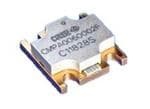
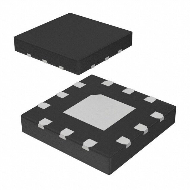
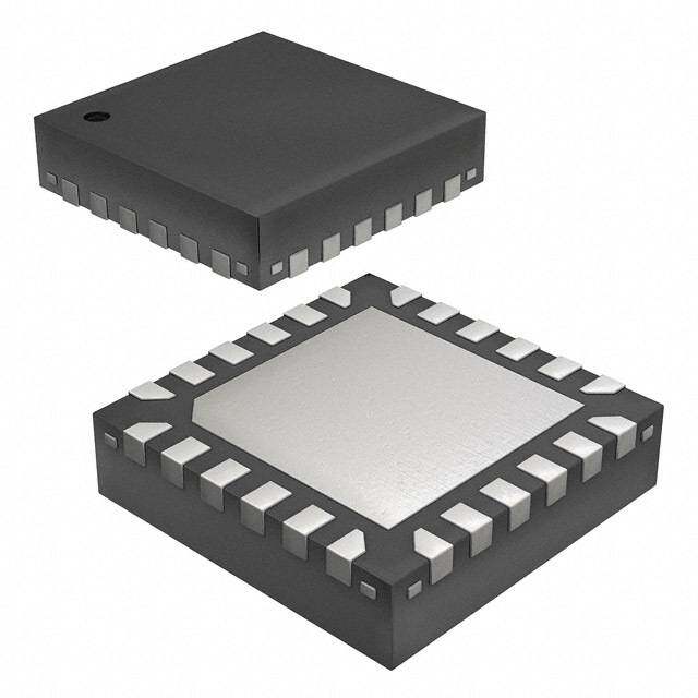
| 产品图片 |
|
| P1dB | - |
| 产品型号 | CMPA0060002F |
| RF类型 | - |
| rohs | 无铅 / 符合限制有害物质指令(RoHS)规范要求 |
| 产品系列 | GaN |
| 产品目录页面 | |
| 供应商器件封装 | 780019 |
| 包装 | 管件 |
| 噪声系数 | - |
| 增益 | 18.8dB |
| 封装/外壳 | 780019 |
| 标准包装 | 25 |
| 测试频率 | 500MHz |
| 电压-电源 | 2 V ~ 28 V |
| 电流-电源 | - |
| 频率 | 20MHz ~ 6GHz |


- 商务部:美国ITC正式对集成电路等产品启动337调查
- 曝三星4nm工艺存在良率问题 高通将骁龙8 Gen1或转产台积电
- 太阳诱电将投资9.5亿元在常州建新厂生产MLCC 预计2023年完工
- 英特尔发布欧洲新工厂建设计划 深化IDM 2.0 战略
- 台积电先进制程称霸业界 有大客户加持明年业绩稳了
- 达到5530亿美元!SIA预计今年全球半导体销售额将创下新高
- 英特尔拟将自动驾驶子公司Mobileye上市 估值或超500亿美元
- 三星加码芯片和SET,合并消费电子和移动部门,撤换高东真等 CEO
- 三星电子宣布重大人事变动 还合并消费电子和移动部门
- 海关总署:前11个月进口集成电路产品价值2.52万亿元 增长14.8%


PDF Datasheet 数据手册内容提取
CMPA0060002F 2 W, 20 MHz - 6000 MHz, GaN MMIC Power Amplifier Cree’s CMPA0060002F is a gallium nitride (GaN) High Electron Mobility Transistor (HEMT) based monolithic microwave integrated circuit (MMIC). GaN has superior properties compared to silicon or gallium arsenide, including higher breakdown voltage, higher saturated electron drift velocity and higher thermal conductivity. GaN HEMTs also offer greater power density and wider bandwidths compared to Si and GaAs transistors. This MMIC employs a distributed (traveling-wave) amplifier design approach, enabling extremely wide bandwidths to be achieved in a small footprint screw-down package featuring a copper-tungsten heat sink. PN: CMPA0060002F Package Type: 780019 Typical Performance Over 20 MHz - 6.0 GHz (T = 25˚C) C Parameter 20 MHz 0.5 GHz 1.0 GHz 2.0 GHz 3.0 GHz 4.0 GHz 5.0 GHz 6.0 GHz Units Gain 19.9 18.8 17.8 16.8 16.8 17.5 18.5 16.5 dB Saturated Output Power, P 1 4.3 4.1 4.5 4.2 3.7 3.9 4.8 3.7 W SAT Power Gain @ P 1 14.7 13.1 12.6 12.2 12.6 10.9 12.2 9.5 dB SAT PAE @ P 1 34 28 29 28 24 26 33 20 % SAT Note1: P is defined as the RF output power where the device starts to draw positive gate current in the range of 2-4 mA. SAT Note2: V = 28 V, I = 100 mA DD DQ Features Applications • 17 dB Small Signal Gain • Ultra Broadband Amplifiers • 3 W Typical P • Fiber Drivers SAT • Operation up to 28 V • Test Instrumentation • High Breakdown Voltage • EMC Amplifier Drivers • High Temperature Operation • 0.5” x 0.5” total product size 5 1 0 2 y a M – 0 .3 v eR Figure 1. Subject to change without notice. 1 www.cree.com/rf
Absolute Maximum Ratings (not simultaneous) at 25˚C Parameter Symbol Rating Units Drain-source Voltage V 84 VDC DSS Gate-source Voltage V -10, +2 VDC GS Storage Temperature T -65, +150 ˚C STG Operating Junction Temperature T 225 ˚C J Maximum Forward Gate Current I 4 mA GMAX Soldering Temperature1 T 245 ˚C S Screw Torque τ 40 in-oz Thermal Resistance, Junction to Case R 4.3 ˚C/W θJC Case Operating Temperature2,3 T -40, +150 ˚C C Note: 1 Refer to the Application Note on soldering at www.cree.com/RF/Document-Library 2 Measured for the CMPA0060002F at P = 2 W. DISS Electrical Characteristics (Frequency = 20 MHz to 6.0 GHz unless otherwise stated; T = 25˚C) C Characteristics Symbol Min. Typ. Max. Units Conditions DC Characteristics Gate Threshold Voltage1 V -3.8 -3.0 -2.7 V V = 20 V, ∆I = 2 mA (GS)TH DS D Gate Quiescent Voltage V – -2.7 – VDC V = 28 V, I = 100 mA (GS)Q DD DQ Saturated Drain Current I – 1.4 – A V = 6.0 V, V = 2.0 V DC DS GS RF Characteristics Small Signal Gain S21 13.5 17 21.5 dB V = 28 V, I = 100 mA DD DQ Input Return Loss S11 – -9 -5 dB V = 28 V, I = 100 mA DD DQ Output Return Loss S22 – -9 -5 dB V = 28 V, I = 100 mA DD DQ V = 28 V, I = 100 mA, Power Output P 2 3 – W DD DQ OUT Frequency = 4.0 GHz, P = 23 dBm IN V = 28 V, I = 100 mA, Power Added Efficiency PAE – 23 – % DD DQ Frequency = 4.0 GHz, P = 23 dBm IN V = 28 V, I = 100 mA, Power Gain G 10 – – dB DD DQ P Frequency = 4.0 GHz, P = 23 dBm IN No damage at all phase angles, Output Mismatch Stress VSWR – – 5 : 1 Y V = 28 V, I = 100 mA, DD DQ P = 23 dBm IN Notes: 1 The device will draw approximately 20-25 mA at pinch off due to the internal circuit structure. Cree, Inc. Copyright © 2009-2015 Cree, Inc. All rights reserved. The information in this document is subject to change without notice. Cree and the Cree logo are 4600 Silicon Drive registered trademarks of Cree, Inc. Other trademarks, product and company names are the property of their respective owners and do not imply specific Durham, North Carolina, USA 27703 product and/or vendor endorsement, sponsorship or association. USA Tel: +1.919.313.5300 Fax: +1.919.869.2733 2 CMPA0060002F Rev 3.0 www.cree.com/rf
Typical Performance Small Signal Gain and Return Losses vs Frequency at 28 V S21_28V 24 0 22 S21_28V S11_28V S22_28V -2 20 -4 18 -6 B) d ( 16 -8 s s o L B)14 -10 n d ur ain(12 -12 Ret G10 -14 ut p u O 8 -16 ut/ p 6 -18 n I 4 -20 2 -22 0 -24 0 1 2 3 4 5 6 Frequency(GHz) Power Gain vs Frequency at 28V 20 18 16 14 12 B) d n(10 ai G 8 6 Gain(OutputPower=34dBm,28V) 4 Gain(OutputPower=33dBm,28V) 2 0 0.0 1.0 2.0 3.0 4.0 5.0 6.0 Frequency(GHz) Cree, Inc. Copyright © 2009-2015 Cree, Inc. All rights reserved. The information in this document is subject to change without notice. Cree and the Cree logo are 4600 Silicon Drive registered trademarks of Cree, Inc. Other trademarks, product and company names are the property of their respective owners and do not imply specific Durham, North Carolina, USA 27703 product and/or vendor endorsement, sponsorship or association. USA Tel: +1.919.313.5300 Fax: +1.919.869.2733 3 CMPA0060002F Rev 3.0 www.cree.com/rf
Typical Performance Saturated Output Power Performance (P ) vs Frequency SAT Psat_28V Frequency P at 28V P at 28V 40.0 SAT SAT (GHz) (dBm) (W) 39.0 0.02 36.6 4.3 m)m)38.0 0.5 36.2 4.1 BB dd37.0 1.0 36.5 4.5 (( erer ww 1.5 36.8 4.7 oo36.0 PP utut 2.0 36.3 4.2 pp35.0 utut 2.5 35.1 3.3 OO dd34.0 ee 3.0 35.7 3.7 atat aturatur33.0 3.5 34.6 2.9 SS 32.0 4.0 35.9 3.9 4.5 35.7 3.8 31.0 5.0 36.8 4.8 30.0 0.0 1.0 2.0 3.0 4.0 5.0 6.0 5.5 34.8 3.0 Frequency(GHz) 6.0 34.3 2.7 Note: P is defined as the RF output power where the device starts to draw positive gate current in the range of 2-4 mA. SAT PAE at 33 & 34 dBm Output Power vs Frequency at 28 V PAEvsFreq.28V 30% 25% %) ( cy20% n e ci Effi 15% d e d d A r e10% w o P 5% PAEat34dBm,28V PAEat33dBm,28V 0% 0.0 1.0 2.0 3.0 4.0 5.0 6.0 Frequency(GHz) Cree, Inc. Copyright © 2009-2015 Cree, Inc. All rights reserved. The information in this document is subject to change without notice. Cree and the Cree logo are 4600 Silicon Drive registered trademarks of Cree, Inc. Other trademarks, product and company names are the property of their respective owners and do not imply specific Durham, North Carolina, USA 27703 product and/or vendor endorsement, sponsorship or association. USA Tel: +1.919.313.5300 Fax: +1.919.869.2733 4 CMPA0060002F Rev 3.0 www.cree.com/rf
General Device Information The CMPA0060002F is a GaN HEMT MMIC Distributed Driver Amplifier, which operates between 20 MHz - 6.0 GHz. The ampli- fier typically provides 17 dB of small signal gain and 2 W saturated output power with an associated power added efficiency of better than 20 %. The wideband amplifier’s input and output are internally matched to 50 Ohm. The amplifier requires bias from appropriate Bias-T’s, through the RF input and output ports. The CMPA0060002F is provided in a flange package format. The input and output connections are gold plated to enable gold bond wire attach at the next level assembly. The measurements in this data sheet were taken on devices wire-bonded to the test fixture with 2 mil gold bond wires. The CMPA0060002F-AMP and the device were then measured using external Bias-T’s, (Aeroflex: 8800, SMF3-12; TECDIA: AMPT-06M20 or similar), as shown in Figure 2. The Bias-T’s were included in the calibration of the test system. All other losses associated with the test fixture are included in the measurements. VGG VDD RF Out RF In Input Bias T Output Bias T CCMMPPAA20506600000022FF mounted in the test fixture Figure 2. Typical test system setup required for measuring CMPA0060002F-AMP Electrostatic Discharge (ESD) Classifications Parameter Symbol Class Test Methodology Human Body Model HBM 1A (> 250 V) JEDEC JESD22 A114-D Charge Device Model CDM II (200 < 500 V) JEDEC JESD22 C101-C Cree, Inc. Copyright © 2009-2015 Cree, Inc. All rights reserved. The information in this document is subject to change without notice. Cree and the Cree logo are 4600 Silicon Drive registered trademarks of Cree, Inc. Other trademarks, product and company names are the property of their respective owners and do not imply specific Durham, North Carolina, USA 27703 product and/or vendor endorsement, sponsorship or association. USA Tel: +1.919.313.5300 Fax: +1.919.869.2733 5 CMPA0060002F Rev 3.0 www.cree.com/rf
CMPA0060002F-TB Demonstration Amplifier Circuit CMPA0060002F-TB Demonstration Amplifier Circuit Outline Cree, Inc. Copyright © 2009-2015 Cree, Inc. All rights reserved. The information in this document is subject to change without notice. Cree and the Cree logo are 4600 Silicon Drive registered trademarks of Cree, Inc. Other trademarks, product and company names are the property of their respective owners and do not imply specific Durham, North Carolina, USA 27703 product and/or vendor endorsement, sponsorship or association. USA Tel: +1.919.313.5300 Fax: +1.919.869.2733 6 CMPA0060002F Rev 3.0 www.cree.com/rf
CMPA0060002F-AMP Demonstration Amplifier Circuit Bill of Materials Designator Description Qty J1,J2 CONNECTOR, SMA, AMP1052901-1 2 - PCB, TACONIC, RF-35-0100-CH/CH 1 Q1 CMPA0060002F 1 Notes 1 The CMPA0060002F is connected to the PCB with 2.0 mil Au bond wires. 2 An external bias T is required. Product Dimensions CMPA0060002F (Package Type — 780019) Cree, Inc. Copyright © 2009-2015 Cree, Inc. All rights reserved. The information in this document is subject to change without notice. Cree and the Cree logo are 4600 Silicon Drive registered trademarks of Cree, Inc. Other trademarks, product and company names are the property of their respective owners and do not imply specific Durham, North Carolina, USA 27703 product and/or vendor endorsement, sponsorship or association. USA Tel: +1.919.313.5300 Fax: +1.919.869.2733 7 CMPA0060002F Rev 3.0 www.cree.com/rf
Product Ordering Information Order Number Description Unit of Measure Image CMPA0060002F GaN MMIC Each CMPA0060002F-TB Test board without GaN MMIC Each CMPA0060002F-AMP Test board with GaN MMIC installed Each Cree, Inc. Copyright © 2009-2015 Cree, Inc. All rights reserved. The information in this document is subject to change without notice. Cree and the Cree logo are 4600 Silicon Drive registered trademarks of Cree, Inc. Other trademarks, product and company names are the property of their respective owners and do not imply specific Durham, North Carolina, USA 27703 product and/or vendor endorsement, sponsorship or association. USA Tel: +1.919.313.5300 Fax: +1.919.869.2733 8 CMPA0060002F Rev 3.0 www.cree.com/rf
Disclaimer Specifications are subject to change without notice. Cree, Inc. believes the information contained within this data sheet to be accurate and reliable. However, no responsibility is assumed by Cree for its use or for any infringement of patents or other rights of third parties which may result from its use. No license is granted by implication or otherwise under any patent or patent rights of Cree. Cree makes no warranty, representation or guarantee regarding the suitability of its products for any particular purpose. “Typical” parameters are the average values expected by Cree in large quantities and are provided for information purposes only. These values can and do vary in different applications, and actual performance can vary over time. All operating parameters should be validated by customer’s technical experts for each application. Cree products are not designed, intended, or authorized for use as components in applications intended for surgical implant into the body or to support or sustain life, in applications in which the failure of the Cree product could result in personal injury or death, or in applications for the planning, construction, maintenance or direct operation of a nuclear facility. CREE and the CREE logo are registered trademarks of Cree, Inc. For more information, please contact: Cree, Inc. 4600 Silicon Drive Durham, North Carolina, USA 27703 www.cree.com/RF Sarah Miller Marketing Cree, RF Components 1.919.407.5302 Ryan Baker Marketing & Sales Cree, RF Components 1.919.407.7816 Tom Dekker Sales Director Cree, RF Components 1.919.407.5639 Cree, Inc. Copyright © 2009-2015 Cree, Inc. All rights reserved. The information in this document is subject to change without notice. Cree and the Cree logo are 4600 Silicon Drive registered trademarks of Cree, Inc. Other trademarks, product and company names are the property of their respective owners and do not imply specific Durham, North Carolina, USA 27703 product and/or vendor endorsement, sponsorship or association. USA Tel: +1.919.313.5300 Fax: +1.919.869.2733 9 CMPA0060002F Rev 3.0 www.cree.com/rf
Mouser Electronics Authorized Distributor Click to View Pricing, Inventory, Delivery & Lifecycle Information: C ree, Inc.: CMPA0060002F CMPA0060002F-TB