ICGOO在线商城 > 射频/IF 和 RFID > RF 放大器 > BGA3015,115

 Datasheet下载
- 型号: BGA3015,115
- 制造商: NXP Semiconductors
- 库位|库存: xxxx|xxxx
- 要求:
| 数量阶梯 | 香港交货 | 国内含税 |
| +xxxx | $xxxx | ¥xxxx |
查看当月历史价格
查看今年历史价格
BGA3015,115产品简介:
ICGOO电子元器件商城为您提供BGA3015,115由NXP Semiconductors设计生产,在icgoo商城现货销售,并且可以通过原厂、代理商等渠道进行代购。 BGA3015,115价格参考。NXP SemiconductorsBGA3015,115封装/规格:RF 放大器, 射频放大器 IC CATV 5MHz ~ 1GHz SOT-89-3。您可以下载BGA3015,115参考资料、Datasheet数据手册功能说明书,资料中有BGA3015,115 详细功能的应用电路图电压和使用方法及教程。
NXP USA Inc.生产的RF放大器型号BGA3015,115主要应用于高频射频(RF)信号的放大场景,其性能和特性使其适用于以下领域:

1. 无线通信:该型号可用于基站、中继站以及其他无线通信设备中。它能够高效放大射频信号,确保信号传输的质量和覆盖范围。

2. 雷达系统:在军事或民用雷达应用中,BGA3015,115可以作为功率放大器的一部分,提升雷达系统的探测能力和精度。

3. 卫星通信:在卫星地面站或卫星终端设备中,这款放大器可以帮助增强上行链路信号的强度,从而提高数据传输效率。

4. 测试与测量设备:在实验室环境中,该型号可被用于射频信号发生器或其他测试仪器中,以提供稳定且高增益的信号输出。

5. 工业、科学与医疗(ISM)领域:例如微波加热、等离子体生成等需要高频能量的应用场合,此放大器能发挥重要作用。

6. 物联网(IoT)设备:对于需要长距离通信的IoT节点,使用此类高性能RF放大器可以扩展网络覆盖范围并改善连接可靠性。

总之,BGA3015,115凭借其卓越的射频放大能力,在众多需要处理高频信号的技术领域有着广泛的应用前景。
| 参数 | 数值 |
| 产品目录 | |
| 描述 | IC MMIC AMP HI EFF 1.5V SOT89 |
| 产品分类 | |
| 品牌 | NXP Semiconductors |
| 数据手册 | |
| 产品图片 |
|
| P1dB | 18dBm |
| 产品型号 | BGA3015,115 |
| PCN封装 | |
| PCN设计/规格 | |
| RF类型 | CATV |
| rohs | 无铅 / 符合限制有害物质指令(RoHS)规范要求 |
| 产品系列 | - |
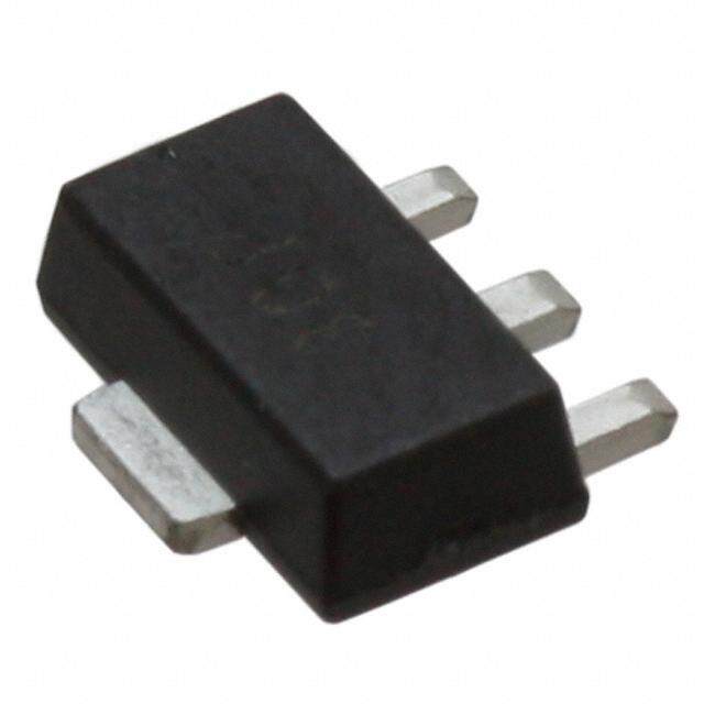
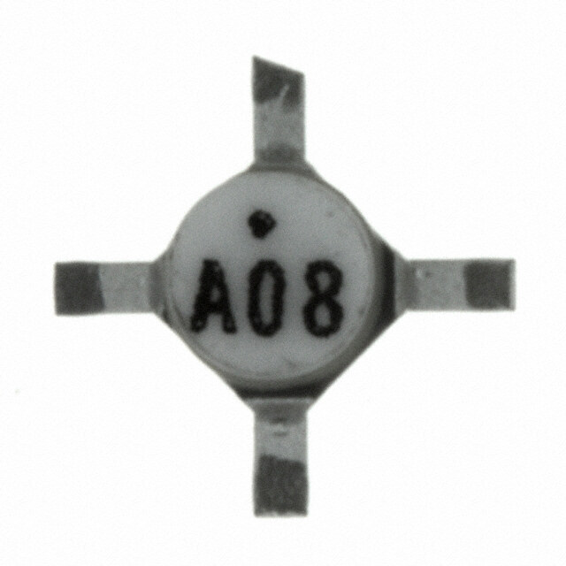
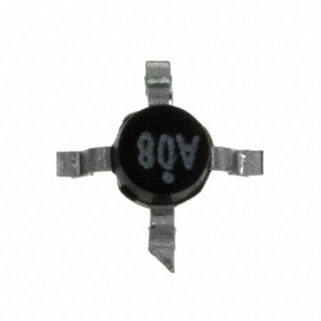
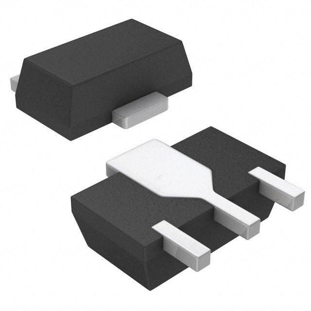
| 供应商器件封装 | SOT-89-3 |
| 其它名称 | 568-10189-2 |
| 包装 | 带卷 (TR) |
| 噪声系数 | 2.6dB |
| 增益 | 15dB |
| 封装/外壳 | TO-243AA |
| 应用说明 | |
| 标准包装 | 1,000 |
| 测试频率 | 1GHz |
| 特色产品 | http://www.digikey.cn/product-highlights/cn/zh/nxp-semiconductors-bga301x-amplifiers/3529 |
| 电压-电源 | 5 V ~ 8 V |
| 电流-电源 | 70mA |
| 频率 | 5MHz ~ 1GHz |
SOT89.jpg)


- 商务部:美国ITC正式对集成电路等产品启动337调查
- 曝三星4nm工艺存在良率问题 高通将骁龙8 Gen1或转产台积电
- 太阳诱电将投资9.5亿元在常州建新厂生产MLCC 预计2023年完工
- 英特尔发布欧洲新工厂建设计划 深化IDM 2.0 战略
- 台积电先进制程称霸业界 有大客户加持明年业绩稳了
- 达到5530亿美元!SIA预计今年全球半导体销售额将创下新高
- 英特尔拟将自动驾驶子公司Mobileye上市 估值或超500亿美元
- 三星加码芯片和SET,合并消费电子和移动部门,撤换高东真等 CEO
- 三星电子宣布重大人事变动 还合并消费电子和移动部门
- 海关总署:前11个月进口集成电路产品价值2.52万亿元 增长14.8%


PDF Datasheet 数据手册内容提取
BGA3018 T89 O S 1 GHz 18 dB gain wideband amplifier MMIC Rev. 3 — 26 September 2013 Product data sheet 1. Product profile 1.1 General description The BGA3018 MMIC is a wideband amplifier with internal biasing. It is designed specifically for high linearity CATV line extenders and drop amplifiers over a frequency range of 5MHz to 1006MHz. The LNA is housed in a lead free 3-pin SOT89 package. 1.2 Features and benefits Internally biased Noise figure of 2.1 dB Flat gain 75 input and output impedance High linearity with an IP3 of 40 dBm and Operating from 5 V to 8 V supply O an IP2 of 60 dBm O 1.3 Applications General wideband amplifiers. CATV return amplifier; frequency ranges of 5 MHz to 300 MHz. CATV infrastructure network driver in optical nodes (FTTx), distribution amplifiers, trunk amplifiers and line extenders in the frequency range from 40 MHz to 1006 MHz. The product is ideally suited for applications as drop amplifiers in CATV distribution systems such as FTTH 1.4 Quick reference data Table 1. Quick refere nce data Bandwidth 40 MHz to 1006 MHz; T =25 C; typical values at V = 8V; Z =Z =75; R1=470; R2=300. amb CC S L Symbol Parameter Conditions Min Typ Max Unit V supply voltage RF input AC coupled 7.6 8 8.4 V CC I total supply current - 120 135 mA CC(tot) T ambient temperature 40 - +85 C amb NF noise figure f = 500 MHz - 2.1 2.6 dB P output power at 1dB gain compression 23.5 25 - dBm L(1dB) IP3 output third-order intercept point [1] 36 40 - dBm O IP2 output second-order intercept point [2] - 60 - dBm O [1] The fundamental frequencies (f1) and (f2) lay between 40 MHz and 1006 MHz. The intermodulation product (IM3) is 2f2f1, where f2=f16MHz. Input power Pi=20dBm. [2] The fundamental frequencies (f1) and (f2) lay between 40 MHz and 1006 MHz. The intermodulation product (IM2) isf2f1, with 40MHz< f1-f2 < 1006MHz. Input power Pi=20dBm.
BGA3018 NXP Semiconductors 1 GHz 18 dB gain wideband amplifier MMIC 2. Pinning information Table 2. Pinning Pin Description Simplified outline Graphic symbol 1 RF_OUT and biasing [1] 2 GND [2] 3 1 3 RF_IN [1] 2 3 2 1 sym130 [1] This pin is DC-coupled and requires an external DC-blocking capacitor. [2] The center metal base of the SOT89 also functions as heatsink for the power amplifier. 3. Ordering information Table 3. Ordering information Type number Package Name Description Version BGA3018 - plastic surface-mounted package; exposed die pad SOT89 for good heattransfer; 3 leads OM7860 EVB 1 GHz 18 dB gain wideband amplifier application - OM7864 EVB 5 MHz to 300 MHz 18 dB reverse amplifier application - OM7868 EVB 40 MHz to 1006 MHz push-pull amplifier application - OM7861 EVB BGA301x wideband variable gain amplifier application - 4. Marking Table 4. Marking codes Type number Marking code Description BGA3018 *6Y * = W : made in China 5. Limiting values Table 5. Limiting values In accordance with the Absolute Maximum Rating System (IEC 60134). Symbol Parameter Conditions Min Max Unit V supply voltage RF input AC coupled 0.6 +15 V CC P input power single tone - 20 dBm i T storage temperature 65 +150 C stg T junction temperature - 150 C j T ambient temperature 40 +85 C amb V electrostatic discharge HumanBodyModel(HBM); 2 - kV ESD voltage AccordingJEDECstandard22-A114E Charged DeviceModel(CDM); 2 - kV AccordingJEDECstandard22-C101B BGA3018 All information provided in this document is subject to legal disclaimers. © NXP B.V. 2013. All rights reserved. Product data sheet Rev. 3 — 26 September 2013 2 of 15
BGA3018 NXP Semiconductors 1 GHz 18 dB gain wideband amplifier MMIC 6. Thermal characteristics Table 6. Thermal characteristics Symbol Parameter Conditions Typ Unit R thermal resistance from junction to solder point 40 K/W th(j-sp) 7. Characteristics 7.1 Forward application Table 7. Characteristics at V = 8 V CC Bandwidth 40 MHz to 1006 MHz; T =25 C; typical values at V = 8 V; Z =Z =75; amb CC S L R1=470; R2=300. Symbol Parameter Conditions Min Typ Max Unit V supply voltage RF input AC coupled 7.6 8 8.4 V CC I total supply current - 120 135 mA CC(tot) s 2 insertion power gain 17 18 19 dB 21 SL slope straight line - 0.5 - dB sl FL flatness of frequency response - 0.5 - dB NF noise figure f = 50 MHz - 1.9 2.4 dB f = 500 MHz - 2.1 2.6 dB f = 1000 MHz - 2.5 3.0 dB RL input return loss f = 50 MHz - 18.5 - dB in f = 500 MHz - 20 - dB f = 1000 MHz - 28 - dB RL output return loss f = 50 MHz - 24 - dB out f = 500 MHz - 28 - dB f = 1000 MHz - 16 - dB P output power at 1dB 23.5 25 - dBm L(1dB) gaincompression IP3 output third-order intercept point [1] 36 40 - dBm O IP2 output second-order intercept point [2] - 60 - dBm O CTB composite triple beat [3] - 75 - dBc CSO composite second-order distortion [3] - 60 - dBc [1] The fundamental frequencies (f ) and (f ) lay between 40 MHz and 1006 MHz. The intermodulation product 1 2 (IM3) is 2f2f1, where f2=f16MHz. Input power Pi=20dBm. [2] The fundamental frequencies (f ) and (f ) lay between 40 MHz and 1006 MHz. The intermodulation product 1 2 (IM2) isf2f1, with 40MHz< f1-f2 < 1006MHz. Input power Pi=20dBm. [3] Measured with 132 NTSC channels V = 30dBmV. O BGA3018 All information provided in this document is subject to legal disclaimers. © NXP B.V. 2013. All rights reserved. Product data sheet Rev. 3 — 26 September 2013 3 of 15
BGA3018 NXP Semiconductors 1 GHz 18 dB gain wideband amplifier MMIC Table 8. Characteristics at V = 5 V CC Bandwidth 40 MHz to 1006 MHz; T =25 C; typical values at V = 5 V; Z =Z =75; amb CC S L R1=470; R2=300. Symbol Parameter Conditions Min Typ Max Unit V supply voltage RF input AC coupled 4.75 5 5.25 V CC I total supply current - 75 85 mA CC(tot) s 2 insertion power gain - 18 - dB 21 SL slope straight line - 0.5 - dB sl FL flatness of frequency response - 0.5 - dB NF noise figure f = 50 MHz - 1.9 - dB f = 500 MHz - 2.2 - dB f = 1000 MHz - 2.5 - dB RL input return loss f = 50 MHz - 18.5 - dB in f = 500 MHz - 18.5 - dB f = 1000 MHz - 28 - dB RL output return loss f = 50 MHz - 26 - dB out f = 500 MHz - 28 - dB f = 1000 MHz - 16 - dB P output power at 1dB - 18 - dBm L(1dB) gaincompression IP3 output third-order intercept point [1] - 36 - dBm O IP2 output second-order intercept point [2] - 54 - dBm O CTB composite triple beat [3] - 70 - dBc CSO composite second-order distortion [3] - 54 - dBc [1] The fundamental frequencies (f ) and (f ) lay between 40 MHz and 1006 MHz. The intermodulation product 1 2 (IM3) is 2f2f1, where f2=f16MHz. Input power Pi=20dBm. [2] The fundamental frequencies (f ) and (f ) lay between 40 MHz and 1006 MHz. The intermodulation product 1 2 (IM2) isf2f1, with 40MHz< f1-f2 < 1006MHz. Input power Pi=20dBm. [3] Measured with 132 NTSC channels V = 30dBmV. O BGA3018 All information provided in this document is subject to legal disclaimers. © NXP B.V. 2013. All rights reserved. Product data sheet Rev. 3 — 26 September 2013 4 of 15
BGA3018 NXP Semiconductors 1 GHz 18 dB gain wideband amplifier MMIC 7.2 Return application Table 9. Characteristics at V = 8 V CC Bandwidth 5 MHz to 300 MHz; T =25 C; typical values at V = 8 V; Z =Z =75; amb CC S L R1=470; R2=300. Symbol Parameter Conditions Min Typ Max Unit V supply voltage RF input AC coupled 7.6 8 8.4 V CC I total supply current - 120 135 mA CC(tot) s 2 insertion power gain - 18 - dB 21 SL slope straight line - 0.5 - dB sl FL flatness of frequency response - 0.5 - dB NF noise figure f = 50 MHz - 1.9 - dB RL input return loss f = 5 MHz - 18.5 - dB in f = 100 MHz - 18.5 - dB f = 200 MHz - 18.5 - dB f = 300 MHz - 18.5 - dB RL output return loss f = 5 MHz - 18.5 - dB out f = 100 MHz - 18.5 - dB f = 200 MHz - 18.5 - dB f = 300 MHz - 18.5 - dB P output power at 1dB - 25 - dBm L(1dB) gaincompression IP3 output third-order intercept point [1] - 40 - dBm O IP2 output second-order intercept point [2] - 60 - dBm O [1] The fundamental frequencies (f ) and (f ) lay between 5 MHz and 300 MHz. The intermodulation product 1 2 (IM3) is 2f2f1, where f2=f16MHz. Input power Pi=20dBm. [2] The fundamental frequencies (f ) and (f ) lay between 5 MHz and 300 MHz. The intermodulation product 1 2 (IM2) isf2f1, with 40MHz<f1-f2<300MHz. Input power Pi=20dBm. BGA3018 All information provided in this document is subject to legal disclaimers. © NXP B.V. 2013. All rights reserved. Product data sheet Rev. 3 — 26 September 2013 5 of 15
BGA3018 NXP Semiconductors 1 GHz 18 dB gain wideband amplifier MMIC Table 10. Characteristics at V = 5 V CC Bandwidth 5 MHz to 300 MHz; T =25 C; typical values at V = 5 V; Z =Z =75; amb CC S L R1=470; R2=300. Symbol Parameter Conditions Min Typ Max Unit V supply voltage RF input AC coupled 4.75 5 5.25 V CC I total supply current - 75 85 mA CC(tot) s 2 insertion power gain - 18 - dB 21 SL slope straight line - 0.5 - dB sl FL flatness of frequency response - 0.5 - dB NF noise figure f = 50 MHz - 1.9 - dB RL input return loss f = 5 MHz - 18.5 - dB in f = 100 MHz - 18.5 - dB f = 200 MHz - 18.5 - dB f = 300 MHz - 18.5 - dB RL output return loss f = 5 MHz - 18.5 - dB out f = 100 MHz - 18.5 - dB f = 200 MHz - 18.5 - dB f = 300 MHz - 18.5 - dB P output power at 1dB - 20 - dBm L(1dB) gaincompression IP3 output third-order intercept point [1] - 36 - dBm O IP2 output second-order intercept point [2] - 54 - dBm O [1] The fundamental frequencies (f ) and (f ) lay between 5 MHz and 300 MHz. The intermodulation product 1 2 (IM3) is 2f2f1, where f2=f16MHz. Input power Pi=20dBm. [2] The fundamental frequencies (f ) and (f ) lay between 5 MHz and 300 MHz. The intermodulation product 1 2 (IM2) isf2f1, with 40MHz<f1-f2<300MHz. Input power Pi=20dBm. BGA3018 All information provided in this document is subject to legal disclaimers. © NXP B.V. 2013. All rights reserved. Product data sheet Rev. 3 — 26 September 2013 6 of 15
BGA3018 NXP Semiconductors 1 GHz 18 dB gain wideband amplifier MMIC 8. Application information 8.1 Forward application 40 MHz to 1006 MHz The BGA3018 can be used in other applications. Please contact your local sales representative for more information. Application notes are available on the NXP website. 8.1.1 Forward application circuit (cid:45)(cid:22) (cid:57)(cid:38)(cid:38) (cid:38)(cid:23) (cid:38)(cid:24) (cid:47)(cid:23) (cid:47)(cid:21) (cid:53)(cid:20) (cid:38)(cid:21) (cid:53)(cid:21) (cid:45)(cid:20) (cid:38)(cid:20) (cid:56)(cid:20) (cid:38)(cid:22) (cid:45)(cid:21) (cid:47)(cid:20) (cid:22) (cid:20) (cid:47)(cid:22) (cid:53)(cid:41)(cid:66)(cid:76)(cid:81) (cid:53)(cid:41)(cid:66)(cid:82)(cid:88)(cid:87) (cid:21) (cid:68)(cid:68)(cid:68)(cid:16)(cid:19)(cid:19)(cid:25)(cid:25)(cid:24)(cid:25) Components are listed in Table11. Fig 1. BGA3018 application circuit All control and supply lines must be decoupled properly. The decoupling capacitors must be placed as close to the device as possible. BGA3018 All information provided in this document is subject to legal disclaimers. © NXP B.V. 2013. All rights reserved. Product data sheet Rev. 3 — 26 September 2013 7 of 15
BGA3018 NXP Semiconductors 1 GHz 18 dB gain wideband amplifier MMIC 8.1.2 Forward application circuit board layout (cid:39) (cid:38) (cid:39) (cid:37)(cid:42)(cid:36)(cid:22)(cid:19)(cid:91)(cid:91)(cid:3)(cid:40)(cid:57)(cid:37) (cid:49) (cid:38) (cid:49) (cid:42) (cid:57) (cid:42) (cid:89)(cid:72)(cid:85)(cid:86)(cid:76)(cid:82)(cid:81)(cid:3)(cid:19)(cid:17)(cid:21) (cid:49)(cid:82)(cid:89)(cid:72)(cid:80)(cid:69)(cid:72)(cid:85)(cid:3)(cid:21)(cid:19)(cid:20)(cid:21) (cid:45)(cid:22) (cid:23)(cid:19)(cid:3)(cid:48)(cid:43)(cid:93)(cid:3)(cid:16)(cid:3)(cid:20)(cid:19)(cid:19)(cid:25)(cid:3)(cid:48)(cid:43)(cid:93) (cid:51)(cid:38)(cid:37)(cid:3)(cid:54)(cid:83)(cid:72)(cid:70)(cid:29)(cid:3)(cid:41)(cid:53)(cid:23)(cid:29)(cid:3)(cid:40)(cid:85)(cid:3)(cid:32)(cid:3)(cid:23)(cid:17)(cid:25) (cid:53)(cid:41)(cid:3)(cid:79)(cid:68)(cid:92)(cid:72)(cid:85)(cid:3)(cid:32)(cid:3)(cid:20)(cid:17)(cid:24)(cid:3)(cid:80)(cid:80)(cid:3)(cid:29)(cid:3)(cid:26)(cid:24)(cid:3)(cid:50)(cid:75)(cid:80) (cid:38)(cid:23) (cid:38)(cid:24) (cid:45)(cid:20) (cid:45)(cid:21) (cid:47)(cid:23) (cid:56)(cid:20) (cid:38)(cid:20) (cid:47)(cid:20) (cid:47)(cid:21) (cid:47)(cid:22) (cid:38)(cid:22) (cid:53)(cid:20) (cid:38)(cid:21) (cid:53)(cid:21) (cid:53)(cid:41)(cid:3)(cid:44)(cid:49) (cid:54)(cid:72)(cid:80)(cid:76)(cid:70)(cid:82)(cid:81)(cid:71)(cid:88)(cid:70)(cid:87)(cid:82)(cid:85)(cid:86) (cid:53)(cid:41)(cid:3)(cid:50)(cid:56)(cid:55) (cid:68)(cid:68)(cid:68)(cid:16)(cid:19)(cid:19)(cid:25)(cid:25)(cid:24)(cid:26) PCB (Printed-Circuit Board) material = FR4; thickness = 1.5mm; size = 40mm40mm; r = 4.6; thickness of copper layer=35 m; Components are listed in Table11. Fig 2. BGA3018 application circuit board layout Table 11. List of comp onents See Figure1 and Figure2. Component Description Value Size Remarks C1, C2, C3, C4 capacitor 10 nF SMD 0402 Murata GRM155R71E103KA01D or capacitor of same quality C5 capacitor 100 pF SMD 0402 Murata GRM1555C1H101JZ01D or capacitor of same quality J1, J2 F-connector 75 - Bomar 861V509ER6 or F-connector of same quality J3 header 3-way - - Molex 90121-0763 or header of the same quality L1, L3 inductor 3.9 nH SMD 0402 Murata LQG15HS3N9S02D or inductor of same quality L2 choke - SMD 0603 Murata BLM18HD182SN1D or choke of same quality L4 inductor 880 nH SMD 1206 Murata LQH31HNR88K03L or inductor of same quality R1 resistor 470 SMD 0402 Yageo RC0402FR-07470RL or resistor of same quality R2 resistor 300 SMD 0402 Yageo RC0402FR-07300RL or resistor of same quality U1 BGA3018 - - NXP BGA3018 All information provided in this document is subject to legal disclaimers. © NXP B.V. 2013. All rights reserved. Product data sheet Rev. 3 — 26 September 2013 8 of 15
BGA3018 NXP Semiconductors 1 GHz 18 dB gain wideband amplifier MMIC 8.2 Return application 5 MHz to 300 MHz The BGA3018 can be used in other applications. Please contact your local sales representative for more information. Application notes are available on the NXP website. 8.2.1 Return application circuit (cid:45)(cid:22) (cid:57)(cid:38)(cid:38) (cid:38)(cid:23) (cid:38)(cid:24) (cid:47)(cid:21) (cid:53)(cid:20) (cid:38)(cid:21) (cid:53)(cid:21) (cid:45)(cid:20) (cid:38)(cid:20) (cid:56)(cid:20) (cid:38)(cid:22) (cid:45)(cid:21) (cid:22) (cid:20) (cid:53)(cid:41)(cid:66)(cid:76)(cid:81) (cid:53)(cid:41)(cid:66)(cid:82)(cid:88)(cid:87) (cid:21) (cid:68)(cid:68)(cid:68)(cid:16)(cid:19)(cid:19)(cid:25)(cid:25)(cid:24)(cid:27) Components are listed in Table11. Fig 3. BGA3018 application circuit All control and supply lines must be decoupled properly. The decoupling capacitors must be placed as close to the device as possible. BGA3018 All information provided in this document is subject to legal disclaimers. © NXP B.V. 2013. All rights reserved. Product data sheet Rev. 3 — 26 September 2013 9 of 15
BGA3018 NXP Semiconductors 1 GHz 18 dB gain wideband amplifier MMIC 8.2.2 Return application circuit board layout (cid:39) (cid:38) (cid:39) (cid:37)(cid:42)(cid:36)(cid:22)(cid:19)(cid:91)(cid:91)(cid:3)(cid:40)(cid:57)(cid:37) (cid:49) (cid:38) (cid:49) (cid:42) (cid:57) (cid:42) (cid:89)(cid:72)(cid:85)(cid:86)(cid:76)(cid:82)(cid:81)(cid:3)(cid:19)(cid:17)(cid:22) (cid:49)(cid:82)(cid:89)(cid:72)(cid:80)(cid:69)(cid:72)(cid:85)(cid:3)(cid:21)(cid:19)(cid:20)(cid:21) (cid:45)(cid:22) (cid:24)(cid:3)(cid:48)(cid:43)(cid:93)(cid:3)(cid:16)(cid:3)(cid:22)(cid:19)(cid:19)(cid:3)(cid:48)(cid:43)(cid:93) (cid:51)(cid:38)(cid:37)(cid:3)(cid:54)(cid:83)(cid:72)(cid:70)(cid:29)(cid:3)(cid:41)(cid:53)(cid:23)(cid:29)(cid:3)(cid:40)(cid:85)(cid:3)(cid:32)(cid:3)(cid:23)(cid:17)(cid:25) (cid:53)(cid:41)(cid:3)(cid:79)(cid:68)(cid:92)(cid:72)(cid:85)(cid:3)(cid:32)(cid:3)(cid:20)(cid:17)(cid:24)(cid:3)(cid:80)(cid:80)(cid:3)(cid:29)(cid:3)(cid:26)(cid:24)(cid:3)(cid:50)(cid:75)(cid:80) (cid:45)(cid:20) (cid:38)(cid:23) (cid:45)(cid:21) (cid:38)(cid:24) (cid:56)(cid:20) (cid:47)(cid:21) (cid:38)(cid:20) (cid:38)(cid:22) (cid:53)(cid:20) (cid:38)(cid:21) (cid:53)(cid:21) (cid:53)(cid:41)(cid:3)(cid:44)(cid:49) (cid:54)(cid:72)(cid:80)(cid:76)(cid:70)(cid:82)(cid:81)(cid:71)(cid:88)(cid:70)(cid:87)(cid:82)(cid:85)(cid:86) (cid:53)(cid:41)(cid:3)(cid:50)(cid:56)(cid:55) (cid:68)(cid:68)(cid:68)(cid:16)(cid:19)(cid:19)(cid:25)(cid:25)(cid:24)(cid:28) PCB (Printed-Circuit Board) material = FR4; thickness = 1.5mm; size = 40mm40mm; r = 4.6; thickness of copper layer=35 m; Components are listed in Table11. Fig 4. BGA3018 application circuit board layout Table 12. List of comp onents See Figure1 and Figure2. Component Description Value Size Remarks C1, C2, C3, C4 capacitor 10 nF SMD 0402 Murata GRM155R71E103KA01D or capacitor of same quality C5 capacitor 100 pF SMD 0402 Murata GRM1555C1H101JZ01D or capacitor of same quality J1, J2 F-connector 75 - Bomar 861V509ER6 or F-connector of same quality J3 header 3-way - - Molex 90121-0763 or header of the same quality L2 inductor 22 H SMD 1206 Murata LQH31CN220K03L or inductor of same quality R1 resistor 470 SMD 0402 Yageo RC0402FR-07470RL or resistor of same quality R2 resistor 300 SMD 0402 Yageo RC0402FR-07300RL or resistor of same quality U1 BGA3018 - - NXP BGA3018 All information provided in this document is subject to legal disclaimers. © NXP B.V. 2013. All rights reserved. Product data sheet Rev. 3 — 26 September 2013 10 of 15
BGA3018 NXP Semiconductors 1 GHz 18 dB gain wideband amplifier MMIC 9. Package outline Plastic surface-mounted package; exposed die pad for good heat transfer; 3 leads SOT89 D B A bp3 E HE Lp 1 2 3 bp2 c w M B bp1 e1 e 0 2 4 mm scale DIMENSIONS (mm are the original dimensions) UNIT A bp1 bp2 bp3 c D E e e1 HE Lp w 1.6 0.48 0.53 1.8 0.44 4.6 2.6 4.25 1.2 mm 3.0 1.5 0.13 1.4 0.35 0.40 1.4 0.23 4.4 2.4 3.75 0.8 OUTLINE REFERENCES EUROPEAN ISSUE DATE VERSION IEC JEDEC JEITA PROJECTION 06-03-16 SOT89 TO-243 SC-62 06-08-29 Fig 5. Package outline SOT89 (SC-62) BGA3018 All information provided in this document is subject to legal disclaimers. © NXP B.V. 2013. All rights reserved. Product data sheet Rev. 3 — 26 September 2013 11 of 15
BGA3018 NXP Semiconductors 1 GHz 18 dB gain wideband amplifier MMIC 10. Abbreviations Table 13. Abbreviations Acronym Description CATV Community Antenna TeleVision FTTH Fiber To The Home FTTx Fiber To The “x” LNA Low-Noise Amplifier MMIC Monolithic Microwave Integrated Circuit 11. Revision history Table 14. Revision history Document ID Release date Data sheet status Change notice Supersedes BGA3018 v.3 20130926 Product data sheet - BGA3018 v.2 Modifications: • Table3 on page2: Evaluation boards have been added. BGA3018 v.2 20130415 Product data sheet - BGA3018 v.1 BGA3018 v.1 20130319 Preliminary data sheet - - BGA3018 All information provided in this document is subject to legal disclaimers. © NXP B.V. 2013. All rights reserved. Product data sheet Rev. 3 — 26 September 2013 12 of 15
BGA3018 NXP Semiconductors 1 GHz 18 dB gain wideband amplifier MMIC 12. Legal information 12.1 Data sheet status Document status[1][2] Product status[3] Definition Objective [short] data sheet Development This document contains data from the objective specification for product development. Preliminary [short] data sheet Qualification This document contains data from the preliminary specification. Product [short] data sheet Production This document contains the product specification. [1] Please consult the most recently issued document before initiating or completing a design. [2] The term ‘short data sheet’ is explained in section “Definitions”. [3] The product status of device(s) described in this document may have changed since this document was published and may differ in case of multiple devices. The latest product status information is available on the Internet at URLhttp://www.nxp.com. 12.2 Definitions Suitability for use — NXP Semiconductors products are not designed, authorized or warranted to be suitable for use in life support, life-critical or safety-critical systems or equipment, nor in applications where failure or Draft — The document is a draft version only. The content is still under malfunction of an NXP Semiconductors product can reasonably be expected internal review and subject to formal approval, which may result in to result in personal injury, death or severe property or environmental modifications or additions. NXP Semiconductors does not give any damage. NXP Semiconductors and its suppliers accept no liability for representations or warranties as to the accuracy or completeness of inclusion and/or use of NXP Semiconductors products in such equipment or information included herein and shall have no liability for the consequences of applications and therefore such inclusion and/or use is at the customer’s own use of such information. risk. Short data sheet — A short data sheet is an extract from a full data sheet Applications — Applications that are described herein for any of these with the same product type number(s) and title. A short data sheet is intended products are for illustrative purposes only. NXP Semiconductors makes no for quick reference only and should not be relied upon to contain detailed and representation or warranty that such applications will be suitable for the full information. For detailed and full information see the relevant full data specified use without further testing or modification. sheet, which is available on request via the local NXP Semiconductors sales office. In case of any inconsistency or conflict with the short data sheet, the Customers are responsible for the design and operation of their applications full data sheet shall prevail. and products using NXP Semiconductors products, and NXP Semiconductors accepts no liability for any assistance with applications or customer product Product specification — The information and data provided in a Product design. It is customer’s sole responsibility to determine whether the NXP data sheet shall define the specification of the product as agreed between Semiconductors product is suitable and fit for the customer’s applications and NXP Semiconductors and its customer, unless NXP Semiconductors and products planned, as well as for the planned application and use of customer have explicitly agreed otherwise in writing. In no event however, customer’s third party customer(s). Customers should provide appropriate shall an agreement be valid in which the NXP Semiconductors product is design and operating safeguards to minimize the risks associated with their deemed to offer functions and qualities beyond those described in the applications and products. Product data sheet. NXP Semiconductors does not accept any liability related to any default, damage, costs or problem which is based on any weakness or default in the 12.3 Disclaimers customer’s applications or products, or the application or use by customer’s third party customer(s). Customer is responsible for doing all necessary testing for the customer’s applications and products using NXP Limited warranty and liability — Information in this document is believed to Semiconductors products in order to avoid a default of the applications and be accurate and reliable. However, NXP Semiconductors does not give any the products or of the application or use by customer’s third party representations or warranties, expressed or implied, as to the accuracy or customer(s). NXP does not accept any liability in this respect. completeness of such information and shall have no liability for the consequences of use of such information. NXP Semiconductors takes no Limiting values — Stress above one or more limiting values (as defined in responsibility for the content in this document if provided by an information the Absolute Maximum Ratings System of IEC60134) will cause permanent source outside of NXP Semiconductors. damage to the device. Limiting values are stress ratings only and (proper) operation of the device at these or any other conditions above those given in In no event shall NXP Semiconductors be liable for any indirect, incidental, the Recommended operating conditions section (if present) or the punitive, special or consequential damages (including - without limitation - lost Characteristics sections of this document is not warranted. Constant or profits, lost savings, business interruption, costs related to the removal or repeated exposure to limiting values will permanently and irreversibly affect replacement of any products or rework charges) whether or not such the quality and reliability of the device. damages are based on tort (including negligence), warranty, breach of contract or any other legal theory. Terms and conditions of commercial sale — NXP Semiconductors products are sold subject to the general terms and conditions of commercial Notwithstanding any damages that customer might incur for any reason whatsoever, NXP Semiconductors’ aggregate and cumulative liability towards sale, as published at http://www.nxp.com/profile/terms, unless otherwise customer for the products described herein shall be limited in accordance agreed in a valid written individual agreement. In case an individual with the Terms and conditions of commercial sale of NXP Semiconductors. agreement is concluded only the terms and conditions of the respective agreement shall apply. NXP Semiconductors hereby expressly objects to Right to make changes — NXP Semiconductors reserves the right to make applying the customer’s general terms and conditions with regard to the changes to information published in this document, including without purchase of NXP Semiconductors products by customer. limitation specifications and product descriptions, at any time and without notice. This document supersedes and replaces all information supplied prior No offer to sell or license — Nothing in this document may be interpreted or to the publication hereof. construed as an offer to sell products that is open for acceptance or the grant, conveyance or implication of any license under any copyrights, patents or other industrial or intellectual property rights. BGA3018 All information provided in this document is subject to legal disclaimers. © NXP B.V. 2013. All rights reserved. Product data sheet Rev. 3 — 26 September 2013 13 of 15
BGA3018 NXP Semiconductors 1 GHz 18 dB gain wideband amplifier MMIC Export control — This document as well as the item(s) described herein product for such automotive applications, use and specifications, and (b) may be subject to export control regulations. Export might require a prior whenever customer uses the product for automotive applications beyond authorization from competent authorities. NXP Semiconductors’ specifications such use shall be solely at customer’s own risk, and (c) customer fully indemnifies NXP Semiconductors for any Quick reference data — The Quick reference data is an extract of the liability, damages or failed product claims resulting from customer design and product data given in the Limiting values and Characteristics sections of this use of the product for automotive applications beyond NXP Semiconductors’ document, and as such is not complete, exhaustive or legally binding. standard warranty and NXP Semiconductors’ product specifications. Non-automotive qualified products — Unless this data sheet expressly Translations — A non-English (translated) version of a document is for states that this specific NXP Semiconductors product is automotive qualified, reference only. The English version shall prevail in case of any discrepancy the product is not suitable for automotive use. It is neither qualified nor tested between the translated and English versions. in accordance with automotive testing or application requirements. NXP Semiconductors accepts no liability for inclusion and/or use of non-automotive qualified products in automotive equipment or applications. 12.4 Trademarks In the event that customer uses the product for design-in and use in automotive applications to automotive specifications and standards, customer Notice: All referenced brands, product names, service names and trademarks (a) shall use the product without NXP Semiconductors’ warranty of the are the property of their respective owners. 13. Contact information For more information, please visit: http://www.nxp.com For sales office addresses, please send an email to: salesaddresses@nxp.com BGA3018 All information provided in this document is subject to legal disclaimers. © NXP B.V. 2013. All rights reserved. Product data sheet Rev. 3 — 26 September 2013 14 of 15
BGA3018 NXP Semiconductors 1 GHz 18 dB gain wideband amplifier MMIC 14. Contents 1 Product profile. . . . . . . . . . . . . . . . . . . . . . . . . . 1 1.1 General description . . . . . . . . . . . . . . . . . . . . . 1 1.2 Features and benefits. . . . . . . . . . . . . . . . . . . . 1 1.3 Applications . . . . . . . . . . . . . . . . . . . . . . . . . . . 1 1.4 Quick reference data . . . . . . . . . . . . . . . . . . . . 1 2 Pinning information. . . . . . . . . . . . . . . . . . . . . . 2 3 Ordering information. . . . . . . . . . . . . . . . . . . . . 2 4 Marking. . . . . . . . . . . . . . . . . . . . . . . . . . . . . . . . 2 5 Limiting values. . . . . . . . . . . . . . . . . . . . . . . . . . 2 6 Thermal characteristics . . . . . . . . . . . . . . . . . . 3 7 Characteristics. . . . . . . . . . . . . . . . . . . . . . . . . . 3 7.1 Forward application . . . . . . . . . . . . . . . . . . . . . 3 7.2 Return application. . . . . . . . . . . . . . . . . . . . . . . 5 8 Application information. . . . . . . . . . . . . . . . . . . 7 8.1 Forward application 40 MHz to 1006 MHz . . . . 7 8.1.1 Forward application circuit . . . . . . . . . . . . . . . . 7 8.1.2 Forward application circuit board layout. . . . . . 8 8.2 Return application 5 MHz to 300 MHz . . . . . . . 9 8.2.1 Return application circuit . . . . . . . . . . . . . . . . . 9 8.2.2 Return application circuit board layout . . . . . . 10 9 Package outline. . . . . . . . . . . . . . . . . . . . . . . . 11 10 Abbreviations. . . . . . . . . . . . . . . . . . . . . . . . . . 12 11 Revision history. . . . . . . . . . . . . . . . . . . . . . . . 12 12 Legal information. . . . . . . . . . . . . . . . . . . . . . . 13 12.1 Data sheet status . . . . . . . . . . . . . . . . . . . . . . 13 12.2 Definitions. . . . . . . . . . . . . . . . . . . . . . . . . . . . 13 12.3 Disclaimers. . . . . . . . . . . . . . . . . . . . . . . . . . . 13 12.4 Trademarks. . . . . . . . . . . . . . . . . . . . . . . . . . . 14 13 Contact information. . . . . . . . . . . . . . . . . . . . . 14 14 Contents. . . . . . . . . . . . . . . . . . . . . . . . . . . . . . 15 Please be aware that important notices concerning this document and the product(s) described herein, have been included in section ‘Legal information’. © NXP B.V. 2013. All rights reserved. For more information, please visit: http://www.nxp.com For sales office addresses, please send an email to: salesaddresses@nxp.com Date of release: 26 September 2013 Document identifier: BGA3018
Mouser Electronics Authorized Distributor Click to View Pricing, Inventory, Delivery & Lifecycle Information: N XP: BGA3018,115 BGA3015,115