ICGOO在线商城 > 射频/IF 和 RFID > RF 放大器 > HMC789ST89E

 Datasheet下载
- 型号: HMC789ST89E
- 制造商: Hittite
- 库位|库存: xxxx|xxxx
- 要求:
| 数量阶梯 | 香港交货 | 国内含税 |
| +xxxx | $xxxx | ¥xxxx |
查看当月历史价格
查看今年历史价格
HMC789ST89E产品简介:
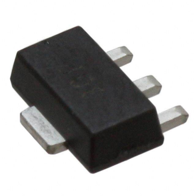
ICGOO电子元器件商城为您提供HMC789ST89E由Hittite设计生产,在icgoo商城现货销售,并且可以通过原厂、代理商等渠道进行代购。 HMC789ST89E价格参考¥42.15-¥71.03。HittiteHMC789ST89E封装/规格:RF 放大器, RF Amplifier IC General Purpose 700MHz ~ 2.8GHz SOT-89。您可以下载HMC789ST89E参考资料、Datasheet数据手册功能说明书,资料中有HMC789ST89E 详细功能的应用电路图电压和使用方法及教程。
HMC789ST89E是Analog Devices Inc.(亚德诺半导体)推出的一款高性能RF放大器,属于宽频带、高线性度的增益模块,主要工作在射频和微波频段。该器件典型工作频率范围为10 MHz至6 GHz,适用于需要宽频带放大能力的系统。

其主要应用场景包括:
1. 无线通信系统:广泛用于蜂窝基站、微波回传链路及5G基础设施中的信号放大,支持多频段操作,有助于提升系统灵活性与性能。
2. 测试与测量设备:作为信号链中的中频或射频增益级,应用于频谱分析仪、信号发生器等精密仪器,提供低噪声和高线性度的信号放大。
3. 国防与航空航天电子系统:适用于雷达、电子战(EW)和通信对抗系统,满足高可靠性与宽温工作的严苛要求。
4. 宽带接收机前端:在软件定义无线电(SDR)和多模式接收机中,作为低失真放大器,保障信号完整性。

HMC789ST89E采用8引脚贴片封装,便于集成于紧凑型高频电路中,具备良好的稳定性和抗干扰能力。其内部集成了匹配网络,简化了设计流程,降低了外围元件需求。此外,该器件具有较高的输出三阶交调点(OIP3),适合处理高动态范围信号,有效减少非线性失真。

综上,HMC789ST89E是一款适用于通信、测试、军工等领域的高性能宽频带RF放大器,特别适合对线性度、带宽和稳定性有较高要求的应用场景。
| 参数 | 数值 |
| 产品目录 | |
| 描述 | IC MMIC AMP HBT DVR AMP SOT-89 |
| 产品分类 | |
| 品牌 | Hittite Microwave Corporation |
| 数据手册 | |
| 产品图片 |
|
| P1dB | 25dBm |
| 产品型号 | HMC789ST89E |
| RF类型 | 通用 |
| rohs | 无铅 / 符合限制有害物质指令(RoHS)规范要求 |
| 产品系列 | - |
| 供应商器件封装 | SOT-89 |
| 其它名称 | 1127-1568 |
| 包装 | 剪切带 (CT) |
| 噪声系数 | 3.8dB |
| 增益 | 18dB |
| 封装/外壳 | TO-243AA |
| 标准包装 | 1 |
| 测试频率 | - |
| 电压-电源 | 5V |
| 电流-电源 | 125mA |
| 频率 | 700MHz ~ 2.8GHz |


- 商务部:美国ITC正式对集成电路等产品启动337调查
- 曝三星4nm工艺存在良率问题 高通将骁龙8 Gen1或转产台积电
- 太阳诱电将投资9.5亿元在常州建新厂生产MLCC 预计2023年完工
- 英特尔发布欧洲新工厂建设计划 深化IDM 2.0 战略
- 台积电先进制程称霸业界 有大客户加持明年业绩稳了
- 达到5530亿美元!SIA预计今年全球半导体销售额将创下新高
- 英特尔拟将自动驾驶子公司Mobileye上市 估值或超500亿美元
- 三星加码芯片和SET,合并消费电子和移动部门,撤换高东真等 CEO
- 三星电子宣布重大人事变动 还合并消费电子和移动部门
- 海关总署:前11个月进口集成电路产品价值2.52万亿元 增长14.8%


PDF Datasheet 数据手册内容提取
HMC789ST89E v02.0314 InGaP HBT GAIN BLOCK MMIC AMPLIFIER, 0.7 -2.8 GHz Typical Applications Features The HMC789ST89E is ideal for: High Output IP3: +42 dBm T • Cellular/4G High Output P1dB: +25 dBm M • Fixed Wireless & WLAN High Gain: 18 dB S • CATV, Cable Modem & DBS Single Supply: +5V - K • Microwave Radio & Test Equipment 45% PAE @ +25 dBm Pout C • IF & RF Applications Industry Standard SOT89 Package O L B Functional Diagram General Description N The HMC789ST89E is a high linearity GaAs InGaP I A HBT gain block MMIC operating from 0.7 to 2.8 GHz G and packaged in an industry standard SOT89 package. Utilizing a minimum number of external components & and a single +5V supply, the amplifier output IP3 can R be optimized to +45 dBm. The high output IP3 and E high gain make the HMC789ST89E ideal for use in V PA driver & pre-driver applications in Cellular/4G and I R Fixed Wireless. D - S R E I F I L P M Electrical Specifications, T = +25°C, Vs= +5V [1] A A Parameter Min. Typ. Max. Min. Typ. Max. Min. Typ. Max. Units Frequency Range 810 - 960 1710 - 1990 2420 - 2700 MHz Gain 17 18 12 13.5 10 11 dB Gain Variation Over Temperature 0.01 0.01 0.01 dB / °C Input Return Loss 12 12 10 dB Output Return Loss 20 15 10 dB Output Power for 1dB Compression (P1dB) 21 23.5 23 25 22 24 dBm Saturated Output Power (Psat) 25.5 27 26 dBm Output Third Order Intercept (IP3) [2] 42 42 42 dBm Noise Figure 3.8 3.8 3.8 dB Supply Current (Icq) 125 150 125 150 125 150 mA [1] Specifications and data reflect HMC789ST89E measured using the respective application circuits for each designated frequency band found herein. Contact the HMC Applications Group for assistance in optimizing performance for your application. [2] Two-tone output power of +10 dBm per tone, 1 MHz spacing. InFfoormra tpiorni cfuern,is hdeed lbivy eArnyal oag nDdev itcoes pisl abcelieev eodr dto ebres a: cHcuirtatteit ean dM reicliarbolew. Haovweev eCr, onor poFroart ipornic,e 2, dEelliivzearby,e atnhd D tor ivpela,c eC horedlemrss: fAonradlo, gM DAe v0ic1e8s2, 4Inc., responsibility is assumed by Analog Devices for its use, nor for any infringements of patents or other One Technology Way, P.O. Box 9106, Norwood, MA 02062-9106 1 rliicgehntss eo fi sth girrda nptaerdti ebsy t himatp mlicPaayht ioroens nuolret of:rto hm9er 7wits8is ue-s 2eu.n5 dS0epre- ca3infi3yc ap4tiao3tne sn ts ou rb Fjpeaactte xtno:t cr9higa7hnt8gs e-o 2wf Ai5thn0oaulo-t g3n oD3tiec7vei3.c eN s o. OPrhdoneer: O78n1--3li2n9e- 4a7t0 0w (cid:127)w Owrd.ehri totnitlein.ec aot mwww.analog.com Trademarks and registered trademarks aArep thpe lpircopaetrityo onf thSeiur rpesppeoctrivte: oPwhneorsn.e: 978-250-33A4p3p l icoart i oanp Spusp@pohrti:t Ptihteon.ceo: 1m-800-ANALOG-D
HMC789ST89E v02.0314 InGaP HBT GAIN BLOCK MMIC AMPLIFIER, 0.7 -2.8 GHz Broadband Gain & Return Loss @ 900 MHz Gain vs. Temperature @ 900 MHz 25 24 22 T 15 M dB) S21 20 S NSE ( 5 SS1212 N (dB) 18 - SPO -5 GAI 16 K E R +25 C C 14 +85 C -15 - 40 C O 12 L -25 10 B 0.4 0.6 0.8 1 1.2 1.4 0.7 0.8 0.9 1 1.1 N FREQUENCY (GHz) FREQUENCY (GHz) I A G Input Return Loss vs. Output Return Loss vs. Temperature @ 900 MHz Temperature @ 900 MHz & 0 0 R E +25 C -5 B) -5 -+ 4805 CC B) V S (d S (d-10 RI S S O O D N L-10 N L-15 R R U U +25 C - RET RET-20 -+ 4805 CC S -15 R -25 E -20 -30 I F 0.7 0.8 0.9 1 1.1 0.7 0.8 0.9 1 1.1 I FREQUENCY (GHz) FREQUENCY (GHz) L P M A P1dB vs. Temperature @ 900 MHz Psat vs. Temperature @ 900 MHz 26 28 25 27 24 26 m) m) P1dB (dB 2223 ++2855 CC Psat (dB 2245 ++2855 CC - 40 C - 40 C 21 23 20 22 0.7 0.8 0.9 1 1.1 0.7 0.8 0.9 1 1.1 FREQUENCY (GHz) FREQUENCY (GHz) InFfoormra tpiorni cfuern,is hdeed lbivy eArnyal oag nDdev itcoes pisl abcelieev eodr dto ebres a: cHcuirtatteit ean dM reicliarbolew. Haovweev eCr, onor poFroart ipornic,e 2, dEelliivzearby,e atnhd D tor ivpela,c eC horedlemrss: fAonradlo, gM DAe v0ic1e8s2, 4Inc., responsibility is assumed by Analog Devices for its use, nor for any infringements of patents or other One Technology Way, P.O. Box 9106, Norwood, MA 02062-9106 rights of third parties that mPayh roesnulet f:ro m9 7its8 u-s2e.5 S0pe-c3ifi3ca4tio3n s s u bFjeact xto: c9ha7n8ge- 2wi5th0ou-t 3no3tic7e3. N o OPrhdoneer: O78n1--3li2n9e- 4a7t0 0w (cid:127)w Owrd.ehri totnitlein.ec aot mwww.analog.com 2 license is granted by implication or otherwise under any patent or patent rights of Analog Devices. Trademarks and registered trademarks aArep thpe lpircopaetrityo onf thSeiur rpesppeoctrivte: oPwhneorsn.e: 978-250-33A4p3p l icoart i oanp Spusp@pohrti:t Ptihteon.ceo: 1m-800-ANALOG-D
HMC789ST89E v02.0314 InGaP HBT GAIN BLOCK MMIC AMPLIFIER, 0.7 -2.8 GHz Output IP3 vs. Temperature @ 900 MHz Output IP3 vs. Pout = 10 dBm Each Tone Output Power @ 900 MHz 50 50 T M 45 45 S K - IP3 (dB) 40 IP3 (dB) 40 C O 35 ++2855 CC 35 -++ 428055 CCC - 40 C L B 30 30 0.7 0.8 0.9 1 1.1 0 2 4 6 8 10 12 14 16 18 N FREQUENCY (GHz) SINGLE TONE POUT (dBm) I A G Reverse Isolation vs. & Noise Figure vs. Temperature @ 900 MHz Temperature @ 900 MHz R 8 0 E +25 C V 6 -+ 4805 CC -10 ++2855 CC RI dB) - 40 C B) N ( D d O - NF ( 4 OLATI-20 S S I 2 -30 R E I 0 -40 F 0.75 0.8 0.85 0.9 0.95 1 0.7 0.8 0.9 1 1.1 I L FREQUENCY (GHz) FREQUENCY (GHz) P M Gain, Power & IP3 vs. A Supply Voltage @ 900 MHz Power Compression @ 900 MHz 50 50 m) B %) P3 (d 40 AE ( 40 GPoauint m), OI Gain dB), P 30 PAE AIN (dB), P1dB (dB 2300 PO1IdPB3 Pout (dBm), GAIN ( 1200 G 10 0 4.5 5 5.5 -8 -4 0 4 8 12 SUPPLY VOLTAGE INPUT POWER (dBm) InFfoormra tpiorni cfuern,is hdeed lbivy eArnyal oag nDdev itcoes pisl abcelieev eodr dto ebres a: cHcuirtatteit ean dM reicliarbolew. Haovweev eCr, onor poFroart ipornic,e 2, dEelliivzearby,e atnhd D tor ivpela,c eC horedlemrss: fAonradlo, gM DAe v0ic1e8s2, 4Inc., responsibility is assumed by Analog Devices for its use, nor for any infringements of patents or other One Technology Way, P.O. Box 9106, Norwood, MA 02062-9106 3 rliicgehntss eo fi sth girrda nptaerdti ebsy t himatp mlicPaayht ioroens nuolret of:rto hm9er 7wits8is ue-s 2eu.n5 dS0epre- ca3infi3yc ap4tiao3tne sn ts ou rb Fjpeaactte xtno:t cr9higa7hnt8gs e-o 2wf Ai5thn0oaulo-t g3n oD3tiec7vei3.c eN s o. OPrhdoneer: O78n1--3li2n9e- 4a7t0 0w (cid:127)w Owrd.ehri totnitlein.ec aot mwww.analog.com Trademarks and registered trademarks aArep thpe lpircopaetrityo onf thSeiur rpesppeoctrivte: oPwhneorsn.e: 978-250-33A4p3p l icoart i oanp Spusp@pohrti:t Ptihteon.ceo: 1m-800-ANALOG-D
HMC789ST89E v02.0314 InGaP HBT GAIN BLOCK MMIC AMPLIFIER, 0.7 -2.8 GHz ACPR vs. Supply Voltage @ 880 MHz CDMA IS95, 9 Channels Forward -20 T -30 M CDMA IS95 -40 FInrteeqguraetniocny: B8W80: 1M.2H2z8 MHz 4.5V S dBc)-50 Forward Link, 9 Channels 5V - CPR (-60 5.5V K A C -70 O -80 L Source ACPR B -90 0 2 4 6 8 10 12 14 16 18 20 22 N CHANNEL POWER (dBm) I A G Broadband Gain & Return Loss @ 1900 MHz Gain vs. Temperature @ 1900 MHz & 20 16 R E V 10 NSE (dB) 0 SSS212112 N (dB) 14 DRI SPO GAI - RE 12 +25 C S -10 +85 C - 40 C R E -20 10 I F 1.2 1.4 1.6 1.8 2 2.2 2.4 2.6 1.7 1.8 1.9 2 2.1 I FREQUENCY (GHz) FREQUENCY (GHz) L P M Input Return Loss vs. Output Return Loss vs. A Temperature @ 1900 MHz Temperature @ 1900 MHz 0 0 S (dB) -4 -++ 428055 CCC S (dB) -5 -++ 428055 CCC S S O O N L -8 N L-10 R R U U ET ET R-12 R-15 -16 -20 1.7 1.8 1.9 2 2.1 1.7 1.8 1.9 2 2.1 FREQUENCY (GHz) FREQUENCY (GHz) InFfoormra tpiorni cfuern,is hdeed lbivy eArnyal oag nDdev itcoes pisl abcelieev eodr dto ebres a: cHcuirtatteit ean dM reicliarbolew. Haovweev eCr, onor poFroart ipornic,e 2, dEelliivzearby,e atnhd D tor ivpela,c eC horedlemrss: fAonradlo, gM DAe v0ic1e8s2, 4Inc., responsibility is assumed by Analog Devices for its use, nor for any infringements of patents or other One Technology Way, P.O. Box 9106, Norwood, MA 02062-9106 rights of third parties that mPayh roesnulet f:ro m9 7its8 u-s2e.5 S0pe-c3ifi3ca4tio3n s s u bFjeact xto: c9ha7n8ge- 2wi5th0ou-t 3no3tic7e3. N o OPrhdoneer: O78n1--3li2n9e- 4a7t0 0w (cid:127)w Owrd.ehri totnitlein.ec aot mwww.analog.com 4 license is granted by implication or otherwise under any patent or patent rights of Analog Devices. Trademarks and registered trademarks aArep thpe lpircopaetrityo onf thSeiur rpesppeoctrivte: oPwhneorsn.e: 978-250-33A4p3p l icoart i oanp Spusp@pohrti:t Ptihteon.ceo: 1m-800-ANALOG-D
HMC789ST89E v02.0314 InGaP HBT GAIN BLOCK MMIC AMPLIFIER, 0.7 -2.8 GHz P1dB vs. Temperature @ 1900 MHz Psat vs. Temperature @ 1900 MHz 28 30 T 27 29 M S m) 26 m) 28 K - P1dB (dB 25 Psat (dB 27 C 24 ++2855 CC 26 ++2855 CC - 40 C - 40 C O 23 25 L B 22 24 1.7 1.8 1.9 2 2.1 1.7 1.8 1.9 2 2.1 N FREQUENCY (GHz) FREQUENCY (GHz) I A G & Output IP3 vs. Temperature @ 1900 MHz Output IP3 vs. Output Power @ 1900 MHz R 50 50 E V 45 45 I R B) B) D d d 3 ( 40 3 ( 40 - IP IP S 35 +25 C 35 +25 C R -+ 4805 CC -+ 4805 CC E I 30 30 F 1.7 1.8 1.9 2 2.1 0 2 4 6 8 10 12 14 16 18 I L FREQUENCY (GHz) SINGLE TONE POUT (dBm) P M Reverse Isolation vs. A Noise Figure vs. Temperature @ 1900 MHz Temperature @ 1900 MHz 8 -10 +25 C 6 -+ 4805 CC -15 ++2855 CC B) - 40 C d B) N ( d O NF ( 4 LATI-20 O S I 2 -25 0 -30 1.7 1.8 1.9 2 2.1 1.7 1.8 1.9 2 2.1 FREQUENCY (GHz) FREQUENCY (GHz) InFfoormra tpiorni cfuern,is hdeed lbivy eArnyal oag nDdev itcoes pisl abcelieev eodr dto ebres a: cHcuirtatteit ean dM reicliarbolew. Haovweev eCr, onor poFroart ipornic,e 2, dEelliivzearby,e atnhd D tor ivpela,c eC horedlemrss: fAonradlo, gM DAe v0ic1e8s2, 4Inc., responsibility is assumed by Analog Devices for its use, nor for any infringements of patents or other One Technology Way, P.O. Box 9106, Norwood, MA 02062-9106 5 rliicgehntss eo fi sth girrda nptaerdti ebsy t himatp mlicPaayht ioroens nuolret of:rto hm9er 7wits8is ue-s 2eu.n5 dS0epre- ca3infi3yc ap4tiao3tne sn ts ou rb Fjpeaactte xtno:t cr9higa7hnt8gs e-o 2wf Ai5thn0oaulo-t g3n oD3tiec7vei3.c eN s o. OPrhdoneer: O78n1--3li2n9e- 4a7t0 0w (cid:127)w Owrd.ehri totnitlein.ec aot mwww.analog.com Trademarks and registered trademarks aArep thpe lpircopaetrityo onf thSeiur rpesppeoctrivte: oPwhneorsn.e: 978-250-33A4p3p l icoart i oanp Spusp@pohrti:t Ptihteon.ceo: 1m-800-ANALOG-D
HMC789ST89E v02.0314 InGaP HBT GAIN BLOCK MMIC AMPLIFIER, 0.7 -2.8 GHz Gain, Power & IP3 vs. Supply Voltage @ 1900 MHz Power Compression @ 1900 MHz 50 50 m) B %) T P3 (d 40 AE ( 40 GPoauint M m), OI Gain dB), P 30 PAE S AIN (dB), P1dB (dB 2300 PO1IdPB3 Pout (dBm), GAIN ( 1200 OCK - G L 10 0 B 4.5 5 5.5 -1 3 7 11 15 19 N SUPPLY VOLTAGE INPUT POWER (dBm) I A G ACPR vs. Supply Voltage @ 1960 MHz ACPR vs. Supply Voltage @ 2140 MHz CDMA 2000, 9 Channels Forward W-CDMA, 64 DPCH & -20 -20 R E -30 -30 CDMA 2000 V CPR (dBc)---654000 FIFnroteerqwguaraerdtnio cLnyin: Bk1W,9 96: 0C1 .Mh2a2Hn8zn MelHsz 4.55VV5.5V CPR (dBc)--5400 WFI6n4rt-ee CDqgDuPraeMCtniHAocny: B2W14: 03 .M84H zMHz 4.5V5V5.5V - DRI A A -60 S -70 Source ACPR R -80 Source ACPR -70 E -90 -80 I F 1 3 5 7 9 11 13 15 17 19 21 0 2 4 6 8 10 12 14 16 18 20 I CHANNEL POWER (dBm) CHANNEL POWER (dBm) L P M Broadband Gain & A Return Loss @ 2600 MHz Gain vs. Temperature @ 2600 MHz 20 14 13 10 B) 12 d NSE ( 0 SSS212112 N (dB) 11 SPO GAI RE 10 +25 C -10 +85 C 9 - 40 C -20 8 2.2 2.3 2.4 2.5 2.6 2.7 2.8 2.9 2.3 2.4 2.5 2.6 2.7 2.8 FREQUENCY (GHz) FREQUENCY (GHz) InFfoormra tpiorni cfuern,is hdeed lbivy eArnyal oag nDdev itcoes pisl abcelieev eodr dto ebres a: cHcuirtatteit ean dM reicliarbolew. Haovweev eCr, onor poFroart ipornic,e 2, dEelliivzearby,e atnhd D tor ivpela,c eC horedlemrss: fAonradlo, gM DAe v0ic1e8s2, 4Inc., responsibility is assumed by Analog Devices for its use, nor for any infringements of patents or other One Technology Way, P.O. Box 9106, Norwood, MA 02062-9106 rights of third parties that mPayh roesnulet f:ro m9 7its8 u-s2e.5 S0pe-c3ifi3ca4tio3n s s u bFjeact xto: c9ha7n8ge- 2wi5th0ou-t 3no3tic7e3. N o OPrhdoneer: O78n1--3li2n9e- 4a7t0 0w (cid:127)w Owrd.ehri totnitlein.ec aot mwww.analog.com 6 license is granted by implication or otherwise under any patent or patent rights of Analog Devices. Trademarks and registered trademarks aArep thpe lpircopaetrityo onf thSeiur rpesppeoctrivte: oPwhneorsn.e: 978-250-33A4p3p l icoart i oanp Spusp@pohrti:t Ptihteon.ceo: 1m-800-ANALOG-D
HMC789ST89E v02.0314 InGaP HBT GAIN BLOCK MMIC AMPLIFIER, 0.7 -2.8 GHz Input Return Loss vs. Output Return Loss vs. Temperature @ 2600 MHz Temperature @ 2600 MHz 0 0 T M dB) -5 -++ 428055 CCC dB) -5 -++ 428055 CCC S OSS (-10 OSS ( - L L-10 N N K UR-15 UR C ET ET R R-15 O -20 L B -25 -20 2.3 2.4 2.5 2.6 2.7 2.8 2.3 2.4 2.5 2.6 2.7 2.8 N FREQUENCY (GHz) FREQUENCY (GHz) I A G & P1dB vs. Temperature @ 2600 MHz Psat vs. Temperature @ 2600 MHz R 26 28 E 27 V 25 RI m) m) 26 S - D P1dB (dB 24 Psat (dB 2245 ++2855 CC 23 +25 C - 40 C R -+ 4805 CC 23 E I 22 22 F 2.3 2.4 2.5 2.6 2.7 2.8 2.3 2.4 2.5 2.6 2.7 2.8 I L FREQUENCY (GHz) FREQUENCY (GHz) P M A Output IP3 vs. Temperature @ 2600 MHz Output IP3 vs. Output Power @ 2600 MHz 50 50 45 45 B) B) d d 3 ( 40 3 ( 40 P P I I 35 +25 C 35 +25 C +85 C +85 C - 40 C - 40 C 30 30 2.3 2.4 2.5 2.6 2.7 2.8 0 2 4 6 8 10 12 14 16 18 FREQUENCY (GHz) SINGLE TONE POUT (dBm) InFfoormra tpiorni cfuern,is hdeed lbivy eArnyal oag nDdev itcoes pisl abcelieev eodr dto ebres a: cHcuirtatteit ean dM reicliarbolew. Haovweev eCr, onor poFroart ipornic,e 2, dEelliivzearby,e atnhd D tor ivpela,c eC horedlemrss: fAonradlo, gM DAe v0ic1e8s2, 4Inc., responsibility is assumed by Analog Devices for its use, nor for any infringements of patents or other One Technology Way, P.O. Box 9106, Norwood, MA 02062-9106 7 rliicgehntss eo fi sth girrda nptaerdti ebsy t himatp mlicPaayht ioroens nuolret of:rto hm9er 7wits8is ue-s 2eu.n5 dS0epre- ca3infi3yc ap4tiao3tne sn ts ou rb Fjpeaactte xtno:t cr9higa7hnt8gs e-o 2wf Ai5thn0oaulo-t g3n oD3tiec7vei3.c eN s o. OPrhdoneer: O78n1--3li2n9e- 4a7t0 0w (cid:127)w Owrd.ehri totnitlein.ec aot mwww.analog.com Trademarks and registered trademarks aArep thpe lpircopaetrityo onf thSeiur rpesppeoctrivte: oPwhneorsn.e: 978-250-33A4p3p l icoart i oanp Spusp@pohrti:t Ptihteon.ceo: 1m-800-ANALOG-D
HMC789ST89E v02.0314 InGaP HBT GAIN BLOCK MMIC AMPLIFIER, 0.7 -2.8 GHz Reverse Isolation vs. Noise Figure vs. Temperature @ 2600 MHz Temperature @ 2600 MHz 8 -10 T +25 C NF (dB) 46 -+ 4805 CC LATION (dB)-15 -++ 428055 CCC K - SM O IS-20 C 2 O L 0 -25 B 2.3 2.4 2.5 2.6 2.7 2.8 2.3 2.4 2.5 2.6 2.7 2.8 N FREQUENCY (GHz) FREQUENCY (GHz) I A G Gain, Power & IP3 vs. Supply Voltage @ 2600 MHz Power Compression @ 2600 MHz & 50 40 R m) B %) E P3 (d 40 AE ( 30 GPoauint V AIN (dB), P1dB (dBm), OI 2300 GPO1aIdPinB3 Pout (dBm), GAIN (dB), P 1200 PAE RS - DRI G E 10 0 I F 4.5 5 5.5 0 5 10 15 20 SUPPLY VOLTAGE INPUT POWER (dBm) LI P M A InFfoormra tpiorni cfuern,is hdeed lbivy eArnyal oag nDdev itcoes pisl abcelieev eodr dto ebres a: cHcuirtatteit ean dM reicliarbolew. Haovweev eCr, onor poFroart ipornic,e 2, dEelliivzearby,e atnhd D tor ivpela,c eC horedlemrss: fAonradlo, gM DAe v0ic1e8s2, 4Inc., responsibility is assumed by Analog Devices for its use, nor for any infringements of patents or other One Technology Way, P.O. Box 9106, Norwood, MA 02062-9106 rights of third parties that mPayh roesnulet f:ro m9 7its8 u-s2e.5 S0pe-c3ifi3ca4tio3n s s u bFjeact xto: c9ha7n8ge- 2wi5th0ou-t 3no3tic7e3. N o OPrhdoneer: O78n1--3li2n9e- 4a7t0 0w (cid:127)w Owrd.ehri totnitlein.ec aot mwww.analog.com 8 license is granted by implication or otherwise under any patent or patent rights of Analog Devices. Trademarks and registered trademarks aArep thpe lpircopaetrityo onf thSeiur rpesppeoctrivte: oPwhneorsn.e: 978-250-33A4p3p l icoart i oanp Spusp@pohrti:t Ptihteon.ceo: 1m-800-ANALOG-D
HMC789ST89E v02.0314 InGaP HBT GAIN BLOCK MMIC AMPLIFIER, 0.7 -2.8 GHz Absolute Maximum Ratings Collector Bias Voltage (Vcc) +6.0 V T RF Input Power (RFIN)(Vs +5Vdc) +18 dBm M Junction Temperature 150 °C S Continuous Pdiss (T = 85 °C) 0.85 W (derate 13.0 mW/°C above 85 °C) - Thermal Resistance K 77 °C/W (junction to ground paddle) C Storage Temperature -65 to +150 °C O Operating Temperature -40 to +85 °C L B N ELECTROSTATIC SENSITIVE DEVICE I OBSERVE HANDLING PRECAUTIONS A G Outline Drawing & R E V I R D - S R E I F I NOTES: L 1. PACKAGE BODY MATERIAL: P MOLDING COMPOUND MP-180S OR EQUIVALENT. M 2. LEAD MATERIAL: Cu w/ Ag SPOT PLATING. 3. LEAD PLATING: 100% MATTE TIN. A 4. DIMENSIONS ARE IN INCHES [MILLIMETERS] 5. DIMENSION DOES NOT INCLUDE MOLDFLASH OF 0.15mm PER SIDE. 6. DIMENSION DOES NOT INCLUDE MOLDFLASH OF 0.25mm PER SIDE. 7. ALL GROUND LEADS MUST BE SOLDERED TO PCB RF GROUND. Package Information Part Number Package Body Material Lead Finish MSL Rating Package Marking [1] HMC789ST89E RoHS-compliant Low Stress Injection Molded Plastic 100% matte Sn MSL1 [2] H789 XXXX [1] 4-Digit lot number XXXX [2] Max peak reflow temperature of 260 °C InFfoormra tpiorni cfuern,is hdeed lbivy eArnyal oag nDdev itcoes pisl abcelieev eodr dto ebres a: cHcuirtatteit ean dM reicliarbolew. Haovweev eCr, onor poFroart ipornic,e 2, dEelliivzearby,e atnhd D tor ivpela,c eC horedlemrss: fAonradlo, gM DAe v0ic1e8s2, 4Inc., responsibility is assumed by Analog Devices for its use, nor for any infringements of patents or other One Technology Way, P.O. Box 9106, Norwood, MA 02062-9106 9 rliicgehntss eo fi sth girrda nptaerdti ebsy t himatp mlicPaayht ioroens nuolret of:rto hm9er 7wits8is ue-s 2eu.n5 dS0epre- ca3infi3yc ap4tiao3tne sn ts ou rb Fjpeaactte xtno:t cr9higa7hnt8gs e-o 2wf Ai5thn0oaulo-t g3n oD3tiec7vei3.c eN s o. OPrhdoneer: O78n1--3li2n9e- 4a7t0 0w (cid:127)w Owrd.ehri totnitlein.ec aot mwww.analog.com Trademarks and registered trademarks aArep thpe lpircopaetrityo onf thSeiur rpesppeoctrivte: oPwhneorsn.e: 978-250-33A4p3p l icoart i oanp Spusp@pohrti:t Ptihteon.ceo: 1m-800-ANALOG-D
HMC789ST89E v02.0314 InGaP HBT GAIN BLOCK MMIC AMPLIFIER, 0.7 -2.8 GHz Pin Descriptions Pin Number Function Description Interface Schematic T This pin is DC coupled. M 1 RFIN Off chip matching components are required. S See Application Circuit herein. - K RF output and DC Bias input for the amplifier. 3 RFOUT Off chip matching components are required. C See Application Circuit herein. O L B These pins & package bottom must be connected to 2, 4 GND RF/DC ground. N I A G & R E V I R D - S R E I F I L P M A InFfoormra tpiorni cfuern,is hdeed lbivy eArnyal oag nDdev itcoes pisl abcelieev eodr dto ebres a: cHcuirtatteit ean dM reicliarbolew. Haovweev eCr, onor poFroart ipornic,e 2, dEelliivzearby,e atnhd D tor ivpela,c eC horedlemrss: fAonradlo, gM DAe v0ic1e8s2, 4Inc., responsibility is assumed by Analog Devices for its use, nor for any infringements of patents or other One Technology Way, P.O. Box 9106, Norwood, MA 02062-9106 rights of third parties that mPayh roesnulet f:ro m9 7its8 u-s2e.5 S0pe-c3ifi3ca4tio3n s s u bFjeact xto: c9ha7n8ge- 2wi5th0ou-t 3no3tic7e3. N o OPrhdoneer: O78n1--3li2n9e- 4a7t0 0w (cid:127)w Owrd.ehri totnitlein.ec aot mwww.analog.com 10 license is granted by implication or otherwise under any patent or patent rights of Analog Devices. Trademarks and registered trademarks aArep thpe lpircopaetrityo onf thSeiur rpesppeoctrivte: oPwhneorsn.e: 978-250-33A4p3p l icoart i oanp Spusp@pohrti:t Ptihteon.ceo: 1m-800-ANALOG-D
HMC789ST89E v02.0314 InGaP HBT GAIN BLOCK MMIC AMPLIFIER, 0.7 -2.8 GHz 900 MHz Application Circuit This circuit was used to specify the performance for 810-960 MHz operation. Contact the HMC Applications Group for assistance in optimizing performance for your application. T M S - K C O L B N I A G & R E V I R D - Recommended Component Values S C1 10 pF R C2 100 pF E C3 100 pF I F C4 1000 pF LI C5 2.2 μF P C6 100 pF M C7 1.2 pF A L1 18 nH L2 3.8 nH InFfoormra tpiorni cfuern,is hdeed lbivy eArnyal oag nDdev itcoes pisl abcelieev eodr dto ebres a: cHcuirtatteit ean dM reicliarbolew. Haovweev eCr, onor poFroart ipornic,e 2, dEelliivzearby,e atnhd D tor ivpela,c eC horedlemrss: fAonradlo, gM DAe v0ic1e8s2, 4Inc., responsibility is assumed by Analog Devices for its use, nor for any infringements of patents or other One Technology Way, P.O. Box 9106, Norwood, MA 02062-9106 11 rliicgehntss eo fi sth girrda nptaerdti ebsy t himatp mlicPaayht ioroens nuolret of:rto hm9er 7wits8is ue-s 2eu.n5 dS0epre- ca3infi3yc ap4tiao3tne sn ts ou rb Fjpeaactte xtno:t cr9higa7hnt8gs e-o 2wf Ai5thn0oaulo-t g3n oD3tiec7vei3.c eN s o. OPrhdoneer: O78n1--3li2n9e- 4a7t0 0w (cid:127)w Owrd.ehri totnitlein.ec aot mwww.analog.com Trademarks and registered trademarks aArep thpe lpircopaetrityo onf thSeiur rpesppeoctrivte: oPwhneorsn.e: 978-250-33A4p3p l icoart i oanp Spusp@pohrti:t Ptihteon.ceo: 1m-800-ANALOG-D
HMC789ST89E v02.0314 InGaP HBT GAIN BLOCK MMIC AMPLIFIER, 0.7 -2.8 GHz 900 MHz Evaluation PCB T M S - K C O L B N I A G & R E V I R D - S R E List of Materials for 900 MHz Evaluation PCB 126222 [1] I F Item Description The circuit board used in this application should use LI RF circuit design techniques. Signal lines should J1 - J2 PCB Mount SMA Connector P J3 2 mm DC Header have 50 Ohm impedance while the package ground M leads and exposed paddle should be connected C1 10 pF Capacitor, 0402 Pkg. A directly to the ground plane similar to that shown. C2 100 pF Capacitor, 0402 Pkg. A sufficient number of via holes should be used C3 100 pF Capacitor, 0402 Pkg. to connect the top and bottom ground planes. C4 1000 pF Capacitor, 0402 Pkg. The evaluation board should be mounted to an C5 2.2 µF Capacitor, Tantalum appropriate heat sink. The evaluation circuit board C6 100 pF Capacitor, 0402 Pkg. shown is available from Hittite upon request. C7 1.2 pF Capacitor, 0402 Pkg. L1 18 nH Inductor, 0402 Pkg. L2 3.8 nH Inductor, 0402 Pkg. U1 HMC789ST89E Linear Amplifier PCB [2] 126220 Evaluation PCB [1] Reference this number when ordering complete evaluation PCB [2] Circuit Board Material: FR4 InFfoormra tpiorni cfuern,is hdeed lbivy eArnyal oag nDdev itcoes pisl abcelieev eodr dto ebres a: cHcuirtatteit ean dM reicliarbolew. Haovweev eCr, onor poFroart ipornic,e 2, dEelliivzearby,e atnhd D tor ivpela,c eC horedlemrss: fAonradlo, gM DAe v0ic1e8s2, 4Inc., responsibility is assumed by Analog Devices for its use, nor for any infringements of patents or other One Technology Way, P.O. Box 9106, Norwood, MA 02062-9106 rights of third parties that mPayh roesnulet f:ro m9 7its8 u-s2e.5 S0pe-c3ifi3ca4tio3n s s u bFjeact xto: c9ha7n8ge- 2wi5th0ou-t 3no3tic7e3. N o OPrhdoneer: O78n1--3li2n9e- 4a7t0 0w (cid:127)w Owrd.ehri totnitlein.ec aot mwww.analog.com 12 license is granted by implication or otherwise under any patent or patent rights of Analog Devices. Trademarks and registered trademarks aArep thpe lpircopaetrityo onf thSeiur rpesppeoctrivte: oPwhneorsn.e: 978-250-33A4p3p l icoart i oanp Spusp@pohrti:t Ptihteon.ceo: 1m-800-ANALOG-D
HMC789ST89E v02.0314 InGaP HBT GAIN BLOCK MMIC AMPLIFIER, 0.7 -2.8 GHz 1900 MHz Application Circuit This circuit was used to specify the performance for 1710-1990 MHz operation. Contact the HMC Applications Group for assistance in optimizing performance for your application. T M S - K C O L B N I A G & R E V I R D Recommended Component Values C1 2.2 pF - C2 5.0 pF S C3 100 pF R C4 1000 pF E I C5 2.2 µF F C6 20 pF I L C7 1.1 pF P L1 20 nH M R1 0.0 Ohm A InFfoormra tpiorni cfuern,is hdeed lbivy eArnyal oag nDdev itcoes pisl abcelieev eodr dto ebres a: cHcuirtatteit ean dM reicliarbolew. Haovweev eCr, onor poFroart ipornic,e 2, dEelliivzearby,e atnhd D tor ivpela,c eC horedlemrss: fAonradlo, gM DAe v0ic1e8s2, 4Inc., responsibility is assumed by Analog Devices for its use, nor for any infringements of patents or other One Technology Way, P.O. Box 9106, Norwood, MA 02062-9106 13 rliicgehntss eo fi sth girrda nptaerdti ebsy t himatp mlicPaayht ioroens nuolret of:rto hm9er 7wits8is ue-s 2eu.n5 dS0epre- ca3infi3yc ap4tiao3tne sn ts ou rb Fjpeaactte xtno:t cr9higa7hnt8gs e-o 2wf Ai5thn0oaulo-t g3n oD3tiec7vei3.c eN s o. OPrhdoneer: O78n1--3li2n9e- 4a7t0 0w (cid:127)w Owrd.ehri totnitlein.ec aot mwww.analog.com Trademarks and registered trademarks aArep thpe lpircopaetrityo onf thSeiur rpesppeoctrivte: oPwhneorsn.e: 978-250-33A4p3p l icoart i oanp Spusp@pohrti:t Ptihteon.ceo: 1m-800-ANALOG-D
HMC789ST89E v02.0314 InGaP HBT GAIN BLOCK MMIC AMPLIFIER, 0.7 -2.8 GHz 1900 MHz Evaluation PCB T M S - K C O L B N I A G & R E V I R D - S R E I F I List of Materials for 1900 MHz Evaluation PCB 126223 [1] L P The circuit board used in this application should use Item Description M RF circuit design techniques. Signal lines should J1 - J2 PCB Mount SMA Connector A have 50 Ohm impedance while the package ground J3 2 mm DC Header leads and exposed paddle should be connected C1 2.2 pF Capacitor, 0402 Pkg. directly to the ground plane similar to that shown. C2 5.0 pF Capacitor, 0402 Pkg. A sufficient number of via holes should be used C3 100 pF Capacitor, 0402 Pkg. to connect the top and bottom ground planes. C4 1000 pF Capacitor, 0402 Pkg. The evaluation board should be mounted to an C5 2.2 µF Capacitor, Tantalum appropriate heat sink. The evaluation circuit board C6 20 pF Capacitor, 0402 Pkg. shown is available from Hittite upon request. C7 1.1 pF Capacitor, 0402 Pkg. L1 18 nH Inductor, 0402 Pkg. R1 0.0 Ohm Resistor, 0402 Pkg. U1 HMC789ST89E Linear Amplifier PCB [2] 126220 Evaluation PCB [1] Reference this number when ordering complete evaluation PCB [2] Circuit Board Material: FR4 InFfoormra tpiorni cfuern,is hdeed lbivy eArnyal oag nDdev itcoes pisl abcelieev eodr dto ebres a: cHcuirtatteit ean dM reicliarbolew. Haovweev eCr, onor poFroart ipornic,e 2, dEelliivzearby,e atnhd D tor ivpela,c eC horedlemrss: fAonradlo, gM DAe v0ic1e8s2, 4Inc., responsibility is assumed by Analog Devices for its use, nor for any infringements of patents or other One Technology Way, P.O. Box 9106, Norwood, MA 02062-9106 rights of third parties that mPayh roesnulet f:ro m9 7its8 u-s2e.5 S0pe-c3ifi3ca4tio3n s s u bFjeact xto: c9ha7n8ge- 2wi5th0ou-t 3no3tic7e3. N o OPrhdoneer: O78n1--3li2n9e- 4a7t0 0w (cid:127)w Owrd.ehri totnitlein.ec aot mwww.analog.com 14 license is granted by implication or otherwise under any patent or patent rights of Analog Devices. Trademarks and registered trademarks aArep thpe lpircopaetrityo onf thSeiur rpesppeoctrivte: oPwhneorsn.e: 978-250-33A4p3p l icoart i oanp Spusp@pohrti:t Ptihteon.ceo: 1m-800-ANALOG-D
HMC789ST89E v02.0314 InGaP HBT GAIN BLOCK MMIC AMPLIFIER, 0.7 -2.8 GHz 2600 MHz Application Circuit This circuit was used to specify the performance for 2420-2700 MHz operation. Contact the HMC Applications Group T for assistance in optimizing performance for your application. M S - K C O L B N I A G & R E V I R D - S R E Recommended Component Values I C1 1.5 pF F I C2 1.5 pF L P C3 100 pF M C4 1000 pF A C5 2.2 µF C6 20 pF C7 0.3 pF L1 18 nH L2 12 nH R1 0.0 Ohm InFfoormra tpiorni cfuern,is hdeed lbivy eArnyal oag nDdev itcoes pisl abcelieev eodr dto ebres a: cHcuirtatteit ean dM reicliarbolew. Haovweev eCr, onor poFroart ipornic,e 2, dEelliivzearby,e atnhd D tor ivpela,c eC horedlemrss: fAonradlo, gM DAe v0ic1e8s2, 4Inc., responsibility is assumed by Analog Devices for its use, nor for any infringements of patents or other One Technology Way, P.O. Box 9106, Norwood, MA 02062-9106 15 rliicgehntss eo fi sth girrda nptaerdti ebsy t himatp mlicPaayht ioroens nuolret of:rto hm9er 7wits8is ue-s 2eu.n5 dS0epre- ca3infi3yc ap4tiao3tne sn ts ou rb Fjpeaactte xtno:t cr9higa7hnt8gs e-o 2wf Ai5thn0oaulo-t g3n oD3tiec7vei3.c eN s o. OPrhdoneer: O78n1--3li2n9e- 4a7t0 0w (cid:127)w Owrd.ehri totnitlein.ec aot mwww.analog.com Trademarks and registered trademarks aArep thpe lpircopaetrityo onf thSeiur rpesppeoctrivte: oPwhneorsn.e: 978-250-33A4p3p l icoart i oanp Spusp@pohrti:t Ptihteon.ceo: 1m-800-ANALOG-D
HMC789ST89E v02.0314 InGaP HBT GAIN BLOCK MMIC AMPLIFIER, 0.7 -2.8 GHz 2600 MHz Evaluation PCB T M S - K C O L B N I A G & R E V I R D - S R E I List of Materials for 2600 MHz Evaluation PCB 125682 [1] F I L The circuit board used in this application should use Item Description P RF circuit design techniques. Signal lines should J1 - J2 PCB Mount SMA Connector M have 50 Ohm impedance while the package ground J3 2 mm DC Header A leads and exposed paddle should be connected C1 1.5 pF Capacitor, 0402 Pkg. directly to the ground plane similar to that shown. C2 1.5 pF Capacitor, 0402 Pkg. A sufficient number of via holes should be used C3 100 pF Capacitor, 0402 Pkg. to connect the top and bottom ground planes. C4 1000 pF Capacitor, 0402 Pkg. The evaluation board should be mounted to an C5 2.2 µF Capacitor, Tantalum appropriate heat sink. The evaluation circuit board C6 20 pF Capacitor, 0402 Pkg. shown is available from Hittite upon request. C7 0.3 pF Capacitor, 0402 Pkg. L1 18 nH Inductor, 0402 Pkg. R1 0.0 Ohm Resistor, 0402 Pkg. U1 HMC789ST89E Linear Amplifier PCB [2] 125220 Evaluation PCB [1] Reference this number when ordering complete evaluation PCB [2] Circuit Board Material: FR4 InFfoormra tpiorni cfuern,is hdeed lbivy eArnyal oag nDdev itcoes pisl abcelieev eodr dto ebres a: cHcuirtatteit ean dM reicliarbolew. Haovweev eCr, onor poFroart ipornic,e 2, dEelliivzearby,e atnhd D tor ivpela,c eC horedlemrss: fAonradlo, gM DAe v0ic1e8s2, 4Inc., responsibility is assumed by Analog Devices for its use, nor for any infringements of patents or other One Technology Way, P.O. Box 9106, Norwood, MA 02062-9106 rights of third parties that mPayh roesnulet f:ro m9 7its8 u-s2e.5 S0pe-c3ifi3ca4tio3n s s u bFjeact xto: c9ha7n8ge- 2wi5th0ou-t 3no3tic7e3. N o OPrhdoneer: O78n1--3li2n9e- 4a7t0 0w (cid:127)w Owrd.ehri totnitlein.ec aot mwww.analog.com 16 license is granted by implication or otherwise under any patent or patent rights of Analog Devices. Trademarks and registered trademarks aArep thpe lpircopaetrityo onf thSeiur rpesppeoctrivte: oPwhneorsn.e: 978-250-33A4p3p l icoart i oanp Spusp@pohrti:t Ptihteon.ceo: 1m-800-ANALOG-D