ICGOO在线商城 > 射频/IF 和 RFID > RF 放大器 > MAX2644EXT+T

 Datasheet下载
- 型号: MAX2644EXT+T
- 制造商: Maxim
- 库位|库存: xxxx|xxxx
- 要求:
| 数量阶梯 | 香港交货 | 国内含税 |
| +xxxx | $xxxx | ¥xxxx |
查看当月历史价格
查看今年历史价格
MAX2644EXT+T产品简介:
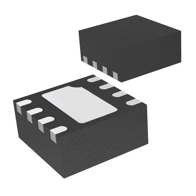
ICGOO电子元器件商城为您提供MAX2644EXT+T由Maxim设计生产,在icgoo商城现货销售,并且可以通过原厂、代理商等渠道进行代购。 MAX2644EXT+T价格参考¥19.08-¥19.08。MaximMAX2644EXT+T封装/规格:RF 放大器, RF Amplifier IC Bluetooth, WLAN 2.4GHz ~ 2.5GHz SC-70-6。您可以下载MAX2644EXT+T参考资料、Datasheet数据手册功能说明书,资料中有MAX2644EXT+T 详细功能的应用电路图电压和使用方法及教程。
MAX2644EXT+T是Maxim Integrated推出的一款高性能RF放大器,主要应用于无线通信系统中的低噪声放大(LNA)。该器件工作频率范围覆盖4.9GHz至5.9GHz,特别适用于5GHz频段的无线局域网(WLAN)系统,如IEEE 802.11a/n/ac标准的Wi-Fi设备。

其典型应用场景包括无线接入点(AP)、路由器、客户端适配器、网卡以及小型蜂窝基站等。MAX2642EXT+T具有高增益(典型值17dB)、低噪声系数(约1.6dB)和优异的线性度(高OIP3),可在保持信号清晰的同时有效增强微弱射频信号,提升接收灵敏度和系统整体性能。

该器件采用紧凑的6引脚SC-70封装,集成输出匹配网络,简化了PCB布局设计,有助于减小终端产品尺寸,适合对空间敏感的便携式或高密度部署设备。此外,它支持单电源供电(通常为3.3V),功耗较低,兼顾性能与能效。

综上所述,MAX2644EXT+T广泛用于需要高性能5GHz频段信号接收的无线通信设备中,是现代高速Wi-Fi系统中关键的前端射频组件之一。
| 参数 | 数值 |
| 产品目录 | |
| 描述 | IC LNA 2.4GHZ SIGE HI-IP3 SC70-6射频放大器 2.4GHz SiGe High Variable IP3 |
| 产品分类 | |
| 品牌 | Maxim Integrated |
| 产品手册 | |
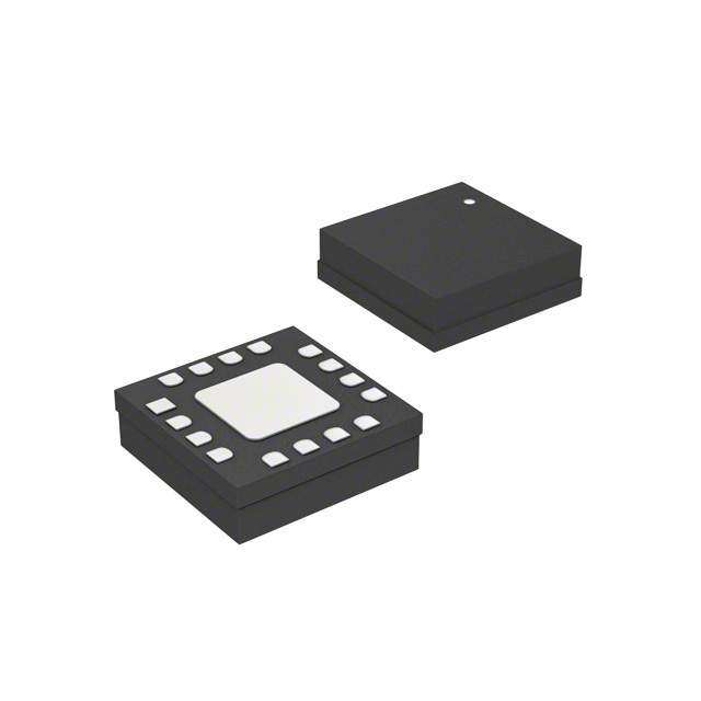
| 产品图片 |
|
| rohs | 符合RoHS无铅 / 符合限制有害物质指令(RoHS)规范要求 |
| 产品系列 | RF集成电路,射频放大器,Maxim Integrated MAX2644EXT+T- |
| 数据手册 | |
| P1dB | -13dBm |
| 产品型号 | MAX2644EXT+T |
| RF类型 | Bluetooth,WLAN |
| 产品培训模块 | http://www.digikey.cn/PTM/IndividualPTM.page?site=cn&lang=zhs&ptm=25703http://www.digikey.cn/PTM/IndividualPTM.page?site=cn&lang=zhs&ptm=25705 |
| 产品种类 | 射频放大器 |
| 供应商器件封装 | SC-70-6 |
| 其它名称 | MAX2644EXT+T-ND |
| 功率增益类型 | 16 dB |
| 包装 | 带卷 (TR) |
| 商标 | Maxim Integrated |
| 噪声系数 | 2dB |
| 增益 | 17dB |
| 安装风格 | SMD/SMT |
| 封装 | Reel |
| 封装/外壳 | 6-TSSOP,SC-88,SOT-363 |
| 封装/箱体 | SOT-70-6 |
| 工作电源电压 | 3 V |
| 工作频率 | 2.4 GHz to 2.5 GHz |
| 工厂包装数量 | 2500 |
| 应用说明 | 点击此处下载产品Datasheet点击此处下载产品Datasheet点击此处下载产品Datasheet点击此处下载产品Datasheet点击此处下载产品Datasheet点击此处下载产品Datasheet点击此处下载产品Datasheet |
| 最大功率耗散 | 245 mW |
| 最大工作温度 | + 85 C |
| 最小工作温度 | - 40 C |
| 标准包装 | 2,500 |
| 测试频率 | 2.45GHz |
| 电压-电源 | 2.7 V ~ 5.5 V |
| 电流-电源 | 2.7mA ~ 7mA |
| 电源电流 | 7 mA |
| 类型 | Low Noise Amplifier |
| 系列 | MAX2644 |
| 输入返回损失 | 15 dB |
| 输出截获点 | - 3 dBm |
| 通道数量 | 1 Channel |
| 隔离分贝 | 30 dB |
| 零件号别名 | MAX2644 |
| 频率 | 2.4GHz ~ 2.5GHz |


- 商务部:美国ITC正式对集成电路等产品启动337调查
- 曝三星4nm工艺存在良率问题 高通将骁龙8 Gen1或转产台积电
- 太阳诱电将投资9.5亿元在常州建新厂生产MLCC 预计2023年完工
- 英特尔发布欧洲新工厂建设计划 深化IDM 2.0 战略
- 台积电先进制程称霸业界 有大客户加持明年业绩稳了
- 达到5530亿美元!SIA预计今年全球半导体销售额将创下新高
- 英特尔拟将自动驾驶子公司Mobileye上市 估值或超500亿美元
- 三星加码芯片和SET,合并消费电子和移动部门,撤换高东真等 CEO
- 三星电子宣布重大人事变动 还合并消费电子和移动部门
- 海关总署:前11个月进口集成电路产品价值2.52万亿元 增长14.8%


PDF Datasheet 数据手册内容提取
EVALUATION KIT AVAILABLE MAX2644 2.4GHz SiGe, High IP3 Low-Noise Amplifier General Description Features The MAX2644 low-cost, high third-order intercept point ● Low Noise Figure (2.0dB at 2450MHz) (IP3) low-noise amplifier (LNA) is designed for applications ● High Gain: 16dB in 2.4GHz WLAN, ISM, and Bluetooth radio systems. It ● Adjustable IP3 and Bias Current features a programmable bias, allowing the input IP3 and supply current to be optimized for specific applications. ● Low-Power Standby Mode The LNA provides up to +1dBm input IP3 while maintaining ● On-Chip Output Matching a low noise figure of 2.0dB and a typical gain of 16dB. ● +2.7V to +5.5V Single-Supply Operation The MAX2644 is designed on a low-noise, advanced ● Ultra-Small 6-Pin SC70 Package silicon-germanium (SiGe) technology. It operates with a +2.7V to +5.5V single supply and is available in an ultra- small 6-pin SC70 package. Applications Ordering Information ● Bluetooth ● 802.11 WLAN PIN- TOP ● Home RF PART TEMP RANGE PACKAGE MARK ● Satellite CD Radio MAX2644EXT+ -40°C to +85°C 6 SC70 AAG ● 2.4GHz ISM Band Radios ● 2.4GHz Cordless Phones MAX2644EXT-T -40°C to +85°C 6 SC70 AAG ● Wireless Local Loop (WLL) MAX2644EXT+T -40°C to +85°C 6 SC70 AAG Typical Operating Circuit Pin Configuration RBIAS VCC 1.2kΩ BIAS VCC TOP VIEW BIAS C1 33pF BIAS 1 6 RFOUT RFIN RFOUT RF INPUT RF OUTPUT MAX2644 GND 2 5 GND L1 3.3nH MAX2644 RFIN 3 4 VCC GND SC70-6 19-1786; Rev 2; 2/17
MAX2644 2.4GHz SiGe, High IP3 Low-Noise Amplifier Absolute Maximum Ratings VCC to GND ............................................................-0.3V to +6V Continuous Power Dissipation (TA = +70°C) RFIN, RFOUT to GND........................................................±0.3V 6-Pin SC70 (derate 3.1mW/°C above +70°C) .............245mW RFIN Power (50Ω source) ................................................+5dBm Storage Temperature ........................................-65°C to +150°C BIAS to GND ..............................................................0 to +0.3V Lead Temperature (soldering, 10s) .................................+300°C Operating Temperature Range ...........................-40°C to +85°C Maximum Junction Temperature .....................................+150°C Stresses beyond those listed under “Absolute Maximum Ratings” may cause permanent damage to the device. These are stress ratings only, and functional operation of the device at these or any other conditions beyond those indicated in the operational sections of the specifications is not implied. Exposure to absolute maximum rating conditions for extended periods may affect device reliability. DC Electrical Characteristics (VCC = +2.7V to +5.5V, RBIAS = 1.2kΩ, no RF signal applied, RFIN and RFOUT are AC-coupled and terminated to 50Ω, TA = -40°C to +85°C. Typical values are at VCC = +3.0V, TA = +25 °C, unless otherwise noted.) (Note 1) PARAMETER CONDITIONS MIN TYP MAX UNITS Supply Voltage 2.7 5.5 V RBIAS = 3.9kΩ 2.7 RBIAS = 1.2kΩ, TA = +25°C 7.0 9.7 Operating Supply Current mA RBIAS = 1.2kΩ, TA = -40°C to +85°C 11.0 RBIAS = 750Ω 10.2 Standby Supply Current RBIAS is unconnected, TA = +25°C, VCC = 3.3V 100 µA AC ELECTRICAL CHARACTERISTICS (MAX2644 EV kit, VCC = +3.0V, fRFIN = 2450MHz, PRFIN = -30dBm, input and output are terminated to 50Ω, RBIAS = 1.2kΩ, TA = +25°C, unless otherwise noted.) (Note 2) PARAMETER CONDITIONS MIN TYP MAX UNITS Operating Frequency (Note 3) 2400 2500 MHz Gain (Note 4) 15 17 dB Gain Variation Over Temperature TA = -40°C to +85°C ±0.7 ±1.0 dB RBIAS = 750Ω -4 Input Third-Order Intercept Point (Note 5) RBIAS = 1.2kΩ -3 dBm RBIAS = 3.9kΩ -8 Input 1dB Compression Point -13 dBm Noise Figure (Note 6) 2.0 2.5 dB Input Return Loss -15 dB Output Return Loss -10 dB Reverse Isolation -30 dB Note 1: Devices are production tested at TA = +25°C. Minimum and maximum values are guaranteed by design and characteriza- tion over temperature and supply voltages. Note 2: Min/Max limits are guaranteed by design and characterization. Note 3: The part has been characterized at the specified frequency range. Operation outside this range is possible but not guaranteed. Note 4: Excluding PC board losses (0.3dB at the input and 0.3dB at the output of the MAX2644 EV kit). Note 5: Measured with two input tones (f1 = 2445MHz, f2 = 2455MHz) both at -30dBm per tone. Input IP3 can be improved to +1dBm with circuit shown in Figure 2. Note 6: Excluding PC board losses (0.3dB typical at the input of the MAX2644 EV kit). www.maximintegrated.com Maxim Integrated │ 2
MAX2644 2.4GHz SiGe, High IP3 Low-Noise Amplifier Typical Operating Characteristics (PRFIN = -30dBm, ZS = ZL = 50Ω, VCC = +3.0V, fRFIN = 2450MHz, RBIAS = 1.2kΩ, TA = +25°C, unless otherwise noted.) SUPPLY CURRENT vs. SUPPLY VOLTAGE SUPPLY CURRENT vs. RBIAS GAIN vs. SUPPLY VOLTAGE SUPPLY CURRENT (mA) 111486204 RBIAST =A 1=. 2+k2Ω5T°AC = +85°C TA = -40°C MAX2644 toc01 SUPPLY CURRENT (mA) 1159713 TA = +85°CTA = +25°C MAX2644 toc02 GAIN (dB) 1111122256789012 RBIAST =A 1=. 2+k2Ω5°CTA = -40°C TA = +85°C MAX2644 toc03 14 2 3 TA = -40°C 13 0 1 12 2.5 3.0 3.5 4.0 4.5 5.0 5.5 0.5 1.0 1.5 2.0 2.5 3.0 3.5 4.0 2.5 3.0 3.5 4.0 4.5 5.0 5.5 SUPPLY VOLTAGE (V) RBIAS (kΩ) SUPPLY VOLTAGE (V) INPUT AND OUTPUT RETURN LOSS GAIN vs. FREQUENCY GAIN vs. RBIAS vs. FREQUENCY 112890 RBIAS = 1.2kΩ TA = -40°C MAX2644 toc04 1189 TA = -40°C MAX2644 toc05 B) --420 RBIAS = 1.2kΩ MAX2644 toc06 17 17 N (d -6 OUTPUT RETURN LOSS O GAIN (dB) 111456 TA = +25°C TA = +85°C GAIN (dB) 16 TA = +25°C SE ISOLATI --11-208 15 ER 13 V -14 E R 12 14 TA = +85°C -16 INPUT RETURN LOSS 11 -18 10 13 -20 2200 2300 2400 2500 2600 2700 0.5 1.0 1.5 2.0 2.5 3.0 3.5 4.0 2200 2300 2400 2500 2600 2700 FREQUENCY (MHz) RBIAS (kΩ) FREQUENCY (MHz) NOISE FIGURE vs. TEMPERATURE REVERSE ISOLATION vs. FREQUENCY NOISE FIGURE vs. FREQUENCY REVERSE ISOLATION (dB) -----4332200550 RTBAIA =S +=2 15.°2TCkAΩ = +85°C TA = -40°C MAX2644 toc07 NOSIE FIGURE (dB) 1122334.......0505050 RBIAS = 1.2kΩ MAX2644 toc08 NOSIE FIGURE (dB) 1122334.......0505050 RBIAS = 1.2kΩ MAX2644 toc09 -45 0.5 0.5 -50 0 0 2200 2300 2400 2500 2600 2700 2350 2400 2450 2500 2550 -40 -15 10 35 60 85 FREQUENCY (MHz) FREQUENCY (MHz) TEMPERATURE (°C) www.maximintegrated.com Maxim Integrated │ 3
MAX2644 2.4GHz SiGe, High IP3 Low-Noise Amplifier Typical Operating Characteristics (continued) (PRFIN = -30dBm, ZS = ZL = 50Ω, VCC = +3.0V, fRFIN = 2450MHz, RBIAS = 1.2kΩ, TA = +25°C, unless otherwise noted.) OUTPUT POWER vs. INPUT POWER IIP3 vs. RBIAS INPUT P1dB vs. RBIAS 150 RBIAS = 750Ω MAX2644 toc10 --21 TA = +85°C MAX2644 toc11 --1121 TA = +85°C MAX2644 toc12 Bm) -3 TA = +25°C -13 R (d 0 RBIAS = 1.2kΩ -4 Bm) -14 WE Bm) (dB PUT PO -5 RBIAS = 3.9kΩ IIP3 (d --65 PUT P1d--1165 TA = +25°C OUT -10 TA = -40°C IN -7 -17 -15 TA = -40°C -8 -18 -20 -9 -19 -30 -25 -20 -15 -10 -5 0 0.5 1.0 1.5 2.0 2.5 3.0 3.5 4.0 0.5 1.0 1.5 2.0 2.5 3.0 3.5 4.0 INPUT POWER (dBm) RBIAS (kΩ) RBIAS (kΩ) Pin Descriptions PIN NAME DESCRIPTION 1 BIAS Resistor Bias Control. Connect a resistor, RBIAS, from BIAS to ground. RBIAS sets IP3 and supply current. The current through this pin is approximately 60mV divided by RBIAS (see Applications Information). 2, 5 GND Ground. For optimum performance, provide a low-inductance connection to the ground plane. Amplifier Input. AC-couple to this pin with a DC blocking capacitor. External matching network is required 3 RFIN for optimum performance. 4 VCC sSeucptpiolyn Vfoorl tmagoere. Binyfpoarmssa twioitnh. a capacitor directly to ground at the supply pin. Refer to VCC Line Bypassing 6 RFOUT Amplifier Output. AC-coupled internally. R1 1.2kΩ RFOUT 1 6 BIAS RFOUT SMA U1 MAX2644 GND 2 5 GND GND C1 RFIN 33pF Length = 400mils VCC 3 4 SMA RFIN VCC L1 C3 C2 3.3nH 2.2pF 33pF GAIN: 17dB IIP3: -3dBm Figure 1. High Gain Design www.maximintegrated.com Maxim Integrated │ 4
MAX2644 2.4GHz SiGe, High IP3 Low-Noise Amplifier R1 L2 1.2kΩ 3.9nH RFOUT 1 6 BIAS RFOUT SMA U1 MAX2644 GND 2 5 GND GND C1 RFIN 33pF Length = 400mils VCC 3 4 SMA RFIN VCC L1 C3 C2 3.3nH 15pF 33pF GAIN: 16dB IIP3: +1dBm Figure 2. High Linearity Design BIAS BIAS MAX2644 MAX2644 (a) (b) Figure 3. Recommended MAX2644 Standby Configurations Applications Information VCC Line Bypassing Input Matching Bypassing the VCC line is necessary for optimum gain/ linearity performance. A transmission line and two capacitors Input matching is required for optimum performance. The are required, as shown in the schematics in Figures 1 and 2. MAX2644 requires a simple LC matching network, as The optimum dimensions and positions of the components shown in the Typical Operating Circuit. To further reduce are as follows: the output transmission line dimension is cost and external component count, replace the external 0.532in (length) x 0.012in (width); the distance from C2 to the inductor with a microstrip transmission line. The Typical IC is 0.352in; and the distance from C3 to the IC is 0.041in. Operating Circuit shows the recommended input matching Please refer to Figures 1 and 2 for component values. network for the MAX2644 at 2450MHz. These values are optimized for best simultaneous gain, noise figure, and return loss performance. www.maximintegrated.com Maxim Integrated │ 5
MAX2644 2.4GHz SiGe, High IP3 Low-Noise Amplifier Table 1. MAX2644 Typical Scattering Parameters (R = 750Ω, V = +3.0V, T = +25°C.) BIAS CC A FREQ. S11 S11 PHASE S21 S21 PHASE S12 S12 PHASE S22 S22 PHASE (MHz) MAG (°) MAG (°) MAG (°) MAG (°) 2200 0.3372 -79.36 5.1940 170.97 0.0414 157.19 0.2818 -73.71 2250 0.3098 -70.09 5.3156 166.79 0.0445 146.70 0.2204 -67.13 2300 0.3283 -57.20 5.4281 159.22 0.0469 130.62 0.1566 -50.26 2350 0.4005 -50.46 5.4175 150.70 0.0441 108.72 0.1480 -3.96 2400 0.4839 -50.28 5.3346 143.93 0.0349 85.67 0.2795 15.12 2450 0.5443 -56.33 5.0687 136.45 0.0233 58.80 0.4179 11.12 2500 0.5758 -60.09 4.9556 132.16 0.0113 27.74 0.5135 3.28 2550 0.5784 -63.61 4.5952 127.68 0.0041 -38.98 0.5622 -2.66 2600 0.5698 -66.56 4.2364 126.58 0.0063 -110.49 0.5986 -7.45 2650 0.5600 -68.51 4.1376 126.51 0.0103 -128.93 0.6208 -10.43 2700 0.5533 -69.86 4.0729 120.60 0.0133 -140.21 0.6425 -12.93 Table 2. MAX2644 Typical Scattering Parameters (R = 1.2kΩ, V = +3.0V, T = +25°C.) BIAS CC A FREQ. S11 S11 PHASE S21 S21 PHASE S12 S12 PHASE S22 S22 PHASE (MHz) MAG (°) MAG (°) MAG (°) MAG (°) 2200 0.3482 -67.06 5.2390 -177.33 0.0402 161.53 0.2873 -76.58 2250 0.3121 -58.60 5.3790 178.72 0.0435 151.97 0.2305 -69.42 2300 0.3051 -43.64 5.5982 173.43 0.0452 136.90 0.1735 -54.22 2350 0.3693 -30.34 5.8137 166.48 0.0427 116.57 0.1582 -16.42 2400 0.4769 -29.48 5.8063 158.29 0.0341 95.13 0.2687 6.52 2450 0.5619 -35.54 5.6624 150.06 0.0236 68.36 0.4043 5.00 2500 0.5948 -42.64 5.3015 142.37 0.0117 41.34 0.5030 -2.19 2550 0.5939 -47.58 4.7813 136.67 0.0034 -13.74 0.5602 -8.04 2600 0.5825 -50.94 4.3271 134.58 0.0056 -104.09 0.5952 -12.76 2650 0.5708 -53.14 4.1961 133.48 0.0096 -124.80 0.6215 -15.97 2700 0.5604 -54.35 4.1068 128.01 0.0125 -134.75 0.6434 -18.83 Standby long VCC lines, it may be necessary to add additional decoupling capacitors. These additional capacitors can Standby mode is achieved by disconnecting BIAS as be located farther away from the device package. Proper shown in Figure 1. Avoid capacitance at the BIAS pin by grounding of the GND pins is essential. If the PC board connecting the bias resistor from BIAS to the switch. uses a topside RF ground, connect it directly to all GND Layout Issues pins. For a board where the ground plane is not on the A properly designed PC board is essential to any RF/ component layer, the best technique is to connect the microwave circuit. Use controlled impedance lines on all GND pins to the board with a plated through-hole located high-frequency inputs and outputs. Bypass with decou- close to the package. pling capacitors located close to the device VCC pin. For www.maximintegrated.com Maxim Integrated │ 6
MAX2644 2.4GHz SiGe, High IP3 Low-Noise Amplifier Table 3. MAX2644 Typical Scattering Parameters (R = 3.9kΩ, V = +3.0V, T = +25°C.) BIAS CC A FREQ. S11 S11 PHASE S21 S21 PHASE S12 S12 PHASE S22 S22 PHASE (MHz) MAG (°) MAG (°) MAG (°) MAG (°) 2200 0.4894 -75.32 3.7368 -173.73 0.0348 156.35 0.2729 -62.97 2250 0.4566 -72.73 3.7718 -177.51 0.0363 147.30 0.2459 -53.68 2300 0.4335 -68.17 3.8855 177.43 0.0369 132.32 0.2211 -41.12 2350 0.4343 -61.46 3.9783 171.34 0.0344 116.21 0.2177 -21.15 2400 0.4695 -57.00 4.0230 165.15 0.0272 95.31 0.2823 -2.41 2450 0.5156 -57.52 4.0087 157.68 0.0179 70.07 0.3924 1.25 2500 0.5403 -61.04 3.8380 149.58 0.0079 42.40 0.4849 -2.71 2550 0.5423 -63.93 3.5140 143.30 0.0018 -46.47 0.5476 -7.30 2600 0.5361 -66.30 3.2048 140.25 0.0055 -112.91 0.5881 -11.35 2650 0.5280 -68.08 3.1204 138.55 0.0100 -132.25 0.6170 -14.57 2700 0.5217 -69.29 3.0860 132.16 0.0121 -133.97 0.6418 -17.44 Table 4. MAX2644 Typical Noise Table 5. MAX2644 Typical Noise Parameters at V = +3.0V, T = +25°C, Parameters at V = +3.0V, T = +25°C, CC A CC A R = 750Ω R = 1.2kΩ BIAS BIAS FRE(QMUHEz)NCY F(dMBIN) │Γopt│ AΓNoGpLt E (RΩN) FRE(QMUHEz)NCY F(dMBIN) │Γopt│ AΓNoGpLt E (RΩN) 2400 1.725 0.361 66.13 24.38 2400 1.570 0.409 69.84 21.77 2450 1.747 0.360 66.93 24.76 2450 1.589 0.408 70.63 21.94 2500 1.769 0.358 67.72 25.14 2500 1.609 0.406 71.63 22.42 Table 6. MAX2644 Typical Noise Chip Information Parameters at V = +3.0V, T = +25°C, TRANSISTOR COUNT: 87 CC A R = 3.9kΩ BIAS FRE(QMUHEz)NCY F(dMBIN) │Γopt│ AΓNoGpLt E (RΩN) 2400 1.497 0.510 86.55 20.58 2450 1.517 0.507 86.50 20.90 2500 1.538 0.504 88.18 21.25 www.maximintegrated.com Maxim Integrated │ 7
MAX2644 2.4GHz SiGe, High IP3 Low-Noise Amplifier Package Information For the latest package outline information and land patterns (footprints), go to www.maximintegrated.com/packages. Note that a “+”, “#”, or “-” in the package code indicates RoHS status only. Package drawings may show a different suffix character, but the drawing pertains to the package regardless of RoHS status. www.maximintegrated.com Maxim Integrated │ 8
MAX2644 2.4GHz SiGe, High IP3 Low-Noise Amplifier Revision History REVISION REVISION PAGES DESCRIPTION NUMBER DATE CHANGED Added MAX2644EXT+, MAX2644EXT-T, and MAX2644EXT-T to Ordering 2 2/17 1 Information table For pricing, delivery, and ordering information, please contact Maxim Direct at 1-888-629-4642, or visit Maxim Integrated’s website at www.maximintegrated.com. Maxim Integrated cannot assume responsibility for use of any circuitry other than circuitry entirely embodied in a Maxim Integrated product. No circuit patent licenses are implied. Maxim Integrated reserves the right to change the circuitry and specifications without notice at any time. The parametric values (min and max limits) shown in the Electrical Characteristics table are guaranteed. Other parametric values quoted in this data sheet are provided for guidance. Maxim Integrated and the Maxim Integrated logo are trademarks of Maxim Integrated Products, Inc. © 2017 Maxim Integrated Products, Inc. │ 9