ICGOO在线商城 > 射频/IF 和 RFID > RF 放大器 > BGU7004,115
 Datasheet下载
- 型号: BGU7004,115
- 制造商: NXP Semiconductors
- 库位|库存: xxxx|xxxx
- 要求:
| 数量阶梯 | 香港交货 | 国内含税 |
| +xxxx | $xxxx | ¥xxxx |
查看当月历史价格
查看今年历史价格
BGU7004,115产品简介:
ICGOO电子元器件商城为您提供BGU7004,115由NXP Semiconductors设计生产,在icgoo商城现货销售,并且可以通过原厂、代理商等渠道进行代购。 BGU7004,115价格参考。NXP SemiconductorsBGU7004,115封装/规格:RF 放大器, 射频放大器 IC Galileo,GLONASS,GPS 1575.42MHz 6-XSON,SOT886(1.45x1)。您可以下载BGU7004,115参考资料、Datasheet数据手册功能说明书,资料中有BGU7004,115 详细功能的应用电路图电压和使用方法及教程。
BGU7004,115 是恩智浦半导体(NXP USA Inc.)生产的一款射频(RF)放大器,主要用于无线通信系统中的信号增强。该器件是一款高线性度、低噪声放大器(LNA),适用于需要高性能射频前端的场景。

其主要应用场景包括:

1. 无线基础设施:如蜂窝基站、微波回传系统等,用于增强接收到的微弱射频信号,提高通信质量和覆盖范围。

2. 工业通信设备:如工业物联网(IIoT)设备、远程监控系统等,适用于需要稳定射频信号传输的工业环境。

3. 测试与测量设备:在射频测试仪器中作为前端放大器,提高测量精度和灵敏度。

4. 广播与多媒体传输:如数字广播、视频传输系统中,用于提升接收灵敏度,确保信号清晰稳定。

5. 汽车通信模块:应用于车载通信系统,如V2X(车联网)设备,以增强无线信号接收能力。

该器件采用先进的硅工艺制造,具有良好的线性性能和低功耗特性,适合在高频段(如GHz级别)工作,广泛应用于现代通信系统中的射频前端模块。
| 参数 | 数值 |
| 产品目录 | |
| 描述 | IC AMP MMIC GPS LNA 6XSON射频放大器 Low Noise Amplifier |
| 产品分类 | |
| 品牌 | NXP Semiconductors |
| 产品手册 | |
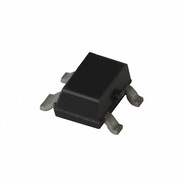
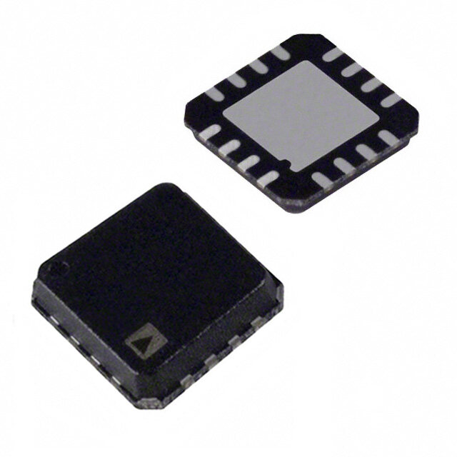
| 产品图片 |
|
| rohs | 符合RoHS无铅 / 符合限制有害物质指令(RoHS)规范要求 |
| 产品系列 | RF集成电路,射频放大器,NXP Semiconductors BGU7004,115- |
| 数据手册 | |
| P1dB | -8dBm |
| 产品型号 | BGU7004,115 |
| PCN封装 | |
| PCN组件/产地 | |
| RF类型 | Galileo,GLONASS,GPS |
| 产品培训模块 | http://www.digikey.cn/PTM/IndividualPTM.page?site=cn&lang=zhs&ptm=25761 |
| 产品种类 | 射频放大器 |
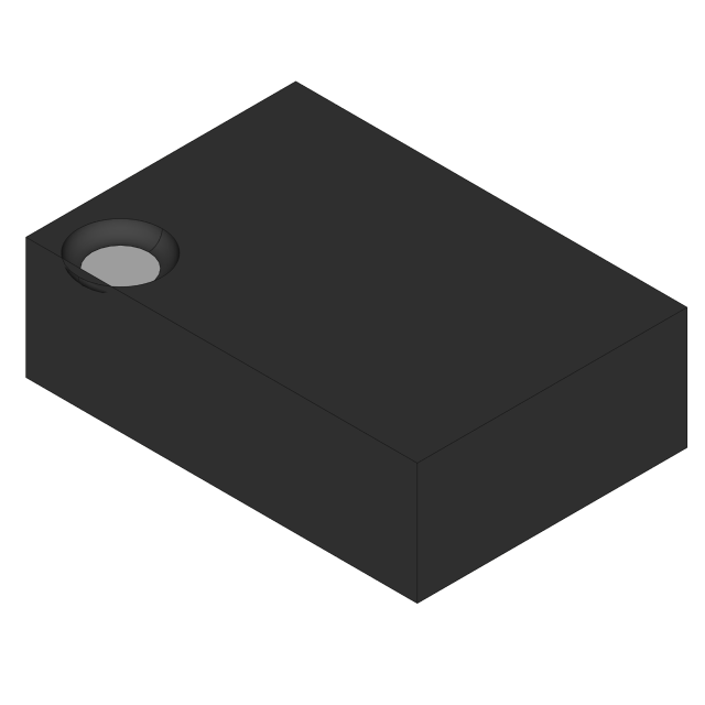
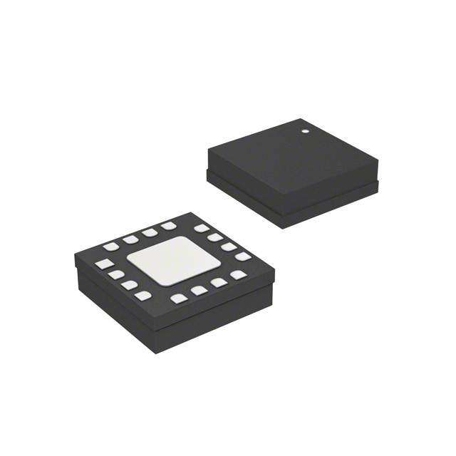
| 供应商器件封装 | 6-XSON,SOT886(1.45x1) |
| 其它名称 | 568-8589-6 |
| 功率增益类型 | 16.5 dB |
| 包装 | Digi-Reel® |
| 商标 | NXP Semiconductors |
| 噪声系数 | 1.3dB |
| 增益 | 21dB |
| 安装风格 | SMD/SMT |
| 封装 | Reel |
| 封装/外壳 | 6-XFDFN |
| 封装/箱体 | XSON-6 |
| 工作电源电压 | 1.8 V |
| 工作频率 | 1.559 GHz to 1.61 GHz |
| 工厂包装数量 | 5000 |
| 最大工作温度 | + 150 C |
| 标准包装 | 1 |
| 测试频率 | 1.85GHz |
| 电压-电源 | 1.5 V ~ 2.85 V |
| 电流-电源 | 11.6mA |
| 电源电流 | 4.5 mA |
| 类型 | Low Noise Amplifier |
| 输出截获点 | 25.5 dBm |
| 频率 | 1575.42MHz |


PDF Datasheet 数据手册内容提取
BGU7004 (cid:59)(cid:54)(cid:50)(cid:49)(cid:25) SiGe:C Low Noise Amplifier MMIC for GPS, GLONASS, Galileo and Compass Rev. 3 — 18 January 2017 Product data sheet 1. Product profile 1.1 General description The BGU7004 is, also known as the GPS1103M, an AEC-Q100 qualified Low Noise Amplifier (LNA) for GNSS receiver applications in a plastic leadless 6-pin, extremely small SOT886 package. The BGU7004 requires only one external matching inductor and one external decoupling capacitor. The BGU7004 adapts itself to the changing environment resulting from co-habitation of different radio systems in modern cellular handsets. It has been designed for low power consumption and optimal performance when jamming signals from co-existing cellular transmitters are present. At low jamming power levels it delivers 16.5 dB gain at a noise figure of 0.85 dB. During high jamming power levels, resulting for example from a cellular transmit burst, it temporarily increases its bias current to improve sensitivity. 1.2 Features and benefits AEC-Q100 qualified (see Section 9.1) Covers full GNSS L1 band, from 1559 MHz to 1610 MHz Noise figure (NF) = 0.85 dB and gain (G ) = 16.5 dB p High input 1 dB compression point P (1dB) of 11 dBm i High out of band IP3 of 9 dBm i Supply voltage 1.5 V to 2.85 V Power-down mode current consumption < 1 A Optimized performance at low supply current of 4.5 mA Integrated matching for the output Requires only one input matching inductor and one supply decoupling capacitor Input and output DC decoupled ESD protection on all pins (HBM > 2 kV) Integrated temperature stabilized bias for easy design Small 6-pin leadless package 1 mm 1.45 mm 0.5 mm 110 GHz transit frequency - SiGe:C technology 1.3 Applications LNA for GPS, GLONASS, Galileo and Compass (BeiDou) in automotive applications like Toll Collection and Emergency Call.
BGU7004 NXP Semiconductors SiGe:C LNA MMIC for GPS, GLONASS, Galileo and Compass LNA for GPS, GLONASS, Galileo and Compass (BeiDou) in smart phones, feature phones, tablet PCs, Personal Navigation Devices, Digital Still Cameras, Digital Video Cameras, RF Front End modules, complete GPS chipset modules and theft protection (laptop, ATM). 1.4 Quick reference data Table 1. Quick reference data f = 1559 MHz to 1610 MHz; V = 1.8 V; P < 40 dBm; T = 25 C; input matched to 50 using CC i amb a 5.6 nH inductor; unless otherwise specified. Symbo Parameter Conditions Min Typ Max Unit l V supply voltage RF input AC coupled 1.5 - 2.85 V CC I supply current V 0.8 V CC ENABLE P < 40 dBm 3.2 4.5 5.7 mA i P = 20 dBm 8.1 11.6 14.4 mA i G power gain P < 40 dBm, no jammer 14 16.5 19 dB p i P = 20 dBm, no jammer 15 17.5 20 dB i NF noise figure P < 40 dBm, no jammer [1] - 0.85 1.2 dB i P < 40 dBm, no jammer [2] - 0.9 1.3 dB i P = 20 dBm, no jammer - 1.2 1.6 dB i P input power at 1 dB f = 1559 MHz to 1610 MHz i(1dB) gain compression V = 1.5 V 15 12 - dBm CC V = 1.8 V 14 11 - dBm CC V = 2.85 V 11 8 - dBm CC IP3 input third-order intercept point f = 1.575 GHz i V = 1.5 V [3] 5 8 - dBm CC V = 1.8 V [3] 5 9 - dBm CC V = 2.85 V [3] 5 12 - dBm CC [1] PCB losses are substracted. [2] Including PCB losses. [3] f1 = 1713 MHz; f2 = 1851 MHz; P1 = P2 = 30 dBm. 2. Pinning information Table 2. Pinning Pin Description Simplified outline Graphic symbol 1 GND (cid:25) (cid:24) (cid:23) (cid:23) (cid:24) 2 GND 3 RF_IN (cid:22) (cid:25) 4 V CC 5 ENABLE (cid:21) (cid:20) (cid:20) (cid:21) (cid:22) (cid:86)(cid:92)(cid:80)(cid:20)(cid:21)(cid:28) 6 RF_OUT (cid:55)(cid:85)(cid:68)(cid:81)(cid:86)(cid:83)(cid:68)(cid:85)(cid:72)(cid:81)(cid:87) (cid:87)(cid:82)(cid:83)(cid:3)(cid:89)(cid:76)(cid:72)(cid:90) BGU7004 All information provided in this document is subject to legal disclaimers. © NXP Semiconductors N.V. 2017. All rights reserved. Product data sheet Rev. 3 — 18 January 2017 2 of 20
BGU7004 NXP Semiconductors SiGe:C LNA MMIC for GPS, GLONASS, Galileo and Compass 3. Ordering information Table 3. Ordering information Type number Package Name Description Version BGU7004 XSON6 plastic extremely thin small outline package; no leads; SOT886 6 terminals; body 1 1.45 0.5 mm 4. Marking Table 4. Marking codes Type number Marking code BGU7004 UY 5. Limiting values Table 5. Limiting values In accordance with the Absolute Maximum Rating System (IEC 60134). Symbol Parameter Conditions Min Max Unit V supply voltage RF input AC coupled 0.5 3.1 V CC V voltage on pin ENABLE V 2.5 V 0.5 3.1 V ENABLE CC V < 2.5 V [2] 0.5 V + 0.6 V CC CC V voltage on pin RF_IN DC RF_IN V 3.0 V [3] 0.5 3.6 V CC V < 3.0 V [2][3] 0.5 V + 0.6 V CC CC V voltage on pin RF_OUT DC RF_OUT V 1.8 V [3] 0.5 3.6 V CC V < 1.8 V [2][3] 0.5 V + 1.8 V CC CC P input power - 0 dBm i P total power dissipation T 130 C [1] 55 mW tot sp T storage temperature 65 150 C stg T junction temperature - 150 C j [1] T is the temperature at the soldering point of the emitter lead. sp [2] Due to internal ESD diode protection, the applied voltage should not exceed the specified maximum in order to avoid excess current. [3] The RF input and RF output are AC coupled through internal DC blocking capacitors. 6. Thermal characteristics Table 6. Thermal characteristics Symbol Parameter Conditions Typ Unit R thermal resistance from junction to solder point 225 K/W th(j-sp) BGU7004 All information provided in this document is subject to legal disclaimers. © NXP Semiconductors N.V. 2017. All rights reserved. Product data sheet Rev. 3 — 18 January 2017 3 of 20
BGU7004 NXP Semiconductors SiGe:C LNA MMIC for GPS, GLONASS, Galileo and Compass 7. Characteristics Table 7. Characterist ics f = 1559 MHz to 1610 MHz; V = 1.8 V; V 0.8 V; P < 40 dBm; T = 25 C; input matched to 50 using a 5.6 nH CC ENABLE i amb inductor; unless otherwise specified. Symbol Parameter Conditions Min Typ Max Unit V supply voltage RF input AC coupled 1.5 - 2.85 V CC I supply current V 0.8 V CC ENABLE P < 40 dBm 3.2 4.5 5.7 mA i P = 20 dBm 8.1 11.6 14.4 mA i V 0.3 V - - 1 A ENABLE T ambient temperature 40 +25 +125 C amb G power gain T = 25 C p amb P < 40 dBm, no jammer 14 16.5 19 dB i P = 20 dBm, no jammer 15 17.5 20 dB i P = 20 dBm; f = 850 MHz 15 17.5 20 dB jam jam P = 20 dBm; f = 1850 MHz 15 17.5 20 dB jam jam 40 C T +125 C amb P < 40 dBm, no jammer 13 - 20 dB i P = 20 dBm, no jammer 14 - 21 dB i P = 20 dBm; f = 850 MHz 14 - 21 dB jam jam P = 20 dBm; f = 1850 MHz 14 - 21 dB jam jam RL input return loss P < 40 dBm 5 8 - dB in i P = 20 dBm 6 10 - dB i RL output return loss P < 40 dBm 10 20 - dB out i P = 20 dBm 10 14 - dB i ISL isolation 20 23 - dB NF noise figure T = 25 C amb P < 40 dBm, no jammer [1] - 0.85 1.2 dB i P < 40 dBm, no jammer [2] - 0.9 1.3 dB i P = 20 dBm, no jammer - 1.2 1.6 dB i P = 20 dBm; f = 850 MHz - 1.1 1.5 dB jam jam P = 20 dBm; f = 1850 MHz - 1.3 1.7 dB jam jam 40 C T +125 C amb P < 40 dBm, no jammer - - 1.8 dB i P = 20 dBm, no jammer - - 2.0 dB i P = 20 dBm; f = 850 MHz - - 1.9 dB jam jam P = 20 dBm; f = 1850 MHz - - 2.1 dB jam jam BGU7004 All information provided in this document is subject to legal disclaimers. © NXP Semiconductors N.V. 2017. All rights reserved. Product data sheet Rev. 3 — 18 January 2017 4 of 20
BGU7004 NXP Semiconductors SiGe:C LNA MMIC for GPS, GLONASS, Galileo and Compass Table 7. Characteristics …continued f = 1559 MHz to 1610 MHz; V = 1.8 V; V 0.8 V; P < 40 dBm; T = 25 C; input matched to 50 using a 5.6 nH CC ENABLE i amb inductor; unless otherwise specified. Symbol Parameter Conditions Min Typ Max Unit P input power at 1 dB f = 1559 MHz to 1610 MHz i(1dB) gain compression V = 1.5 V 15 12 - dBm CC V = 1.8 V 14 11 - dBm CC V = 2.85 V 11 8 - dBm CC f = 806 MHz to 928 MHz V = 1.5 V [3] 15 12 - dBm CC V = 1.8 V [3] 14 11 - dBm CC V = 2.85 V [3] 14 11 - dBm CC f = 1612 MHz to 1909 MHz V = 1.5 V [3] 13 10 - dBm CC V = 1.8 V [3] 12 9 - dBm CC V = 2.85 V [3] 10 7 - dBm CC IP3 input third-order intercept point f = 1.575 GHz i V = 1.5 V [4] 5 8 - dBm CC V = 1.8 V [4] 5 9 - dBm CC V = 2.85 V [4] 5 12 - dBm CC t turn-on time [5] - - 2 s on t turn-off time [5] - - 1 s off K Rollett stability factor 1 - - [1] PCB losses are subtracted. [2] Including PCB losses. [3] Out of band. [4] f1 = 1713 MHz; f2 = 1851 MHz; P1 = P2 = 30 dBm. [5] Within 10 % of the final gain. Table 8. ENABLE (pin 5) 40 C T +125 C; 1.5 V V 2.85 V amb CC V (V) State ENABLE 0.3 OFF 0.8 ON BGU7004 All information provided in this document is subject to legal disclaimers. © NXP Semiconductors N.V. 2017. All rights reserved. Product data sheet Rev. 3 — 18 January 2017 5 of 20
BGU7004 NXP Semiconductors SiGe:C LNA MMIC for GPS, GLONASS, Galileo and Compass 8. Application information 8.1 GNSS LNA (cid:57)(cid:72)(cid:81) (cid:57)(cid:70)(cid:70) (cid:38)(cid:20) (cid:24) (cid:53)(cid:41)(cid:3)(cid:76)(cid:81)(cid:83)(cid:88)(cid:87) (cid:47)(cid:20) (cid:22) (cid:23)(cid:25) (cid:53)(cid:41)(cid:3)(cid:82)(cid:88)(cid:87)(cid:83)(cid:88)(cid:87) (cid:44)(cid:38)(cid:20) (cid:20) (cid:21) (cid:19)(cid:19)(cid:20)(cid:68)(cid:68)(cid:78)(cid:25)(cid:27)(cid:24) For a list of components see Table 9. Fig 1. Schematics GNSS LNA evaluation board T able 9. List of components For schematics see Figure 1. Component Description Value Supplier Remarks C1 decoupling capacitor 1 nF various IC1 BGU7004 - NXP L1 high quality matching inductor 5.6 nH Murata LQW15A (cid:19)(cid:19)(cid:20)(cid:68)(cid:68)(cid:82)(cid:20)(cid:28)(cid:21) (cid:19)(cid:19)(cid:20)(cid:68)(cid:68)(cid:82)(cid:20)(cid:28)(cid:22) (cid:25)(cid:17)(cid:24) (cid:25)(cid:17)(cid:19) (cid:44)(cid:38)(cid:38) (cid:44)(cid:38)(cid:38) (cid:11)(cid:80)(cid:36)(cid:12) (cid:11)(cid:80)(cid:36)(cid:12) (cid:11)(cid:20)(cid:12) (cid:24)(cid:17)(cid:24) (cid:24)(cid:17)(cid:19) (cid:11)(cid:21)(cid:12) (cid:11)(cid:22)(cid:12) (cid:11)(cid:22)(cid:12) (cid:11)(cid:23)(cid:12) (cid:11)(cid:21)(cid:12) (cid:11)(cid:20)(cid:12) (cid:23)(cid:17)(cid:24) (cid:23)(cid:17)(cid:19) (cid:22)(cid:17)(cid:24) (cid:22)(cid:17)(cid:19) (cid:20)(cid:17)(cid:19) (cid:20)(cid:17)(cid:24) (cid:21)(cid:17)(cid:19) (cid:21)(cid:17)(cid:24) (cid:22)(cid:17)(cid:19) (cid:22)(cid:17)(cid:24) (cid:16)(cid:24)(cid:24) (cid:16)(cid:20)(cid:24) (cid:21)(cid:24) (cid:25)(cid:24) (cid:20)(cid:19)(cid:24) (cid:20)(cid:23)(cid:24) (cid:57)(cid:38)(cid:38)(cid:3)(cid:11)(cid:57)(cid:12) (cid:55)(cid:68)(cid:80)(cid:69)(cid:3)(cid:11)(cid:131)(cid:38)(cid:12) Pi = 45 dBm. Pi = 45 dBm. (1) Tamb = 40 C (1) VCC = 1.5 V (2) Tamb = +25 C (2) VCC = 1.8 V (3) Tamb = +85 C (3) VCC = 2.85 V (4) Tamb = +125 C Fig 2. Supply current as a function of supply voltage; Fig 3. Supply current as a function of ambient typical values temperature; typical values BGU7004 All information provided in this document is subject to legal disclaimers. © NXP Semiconductors N.V. 2017. All rights reserved. Product data sheet Rev. 3 — 18 January 2017 6 of 20
BGU7004 NXP Semiconductors SiGe:C LNA MMIC for GPS, GLONASS, Galileo and Compass (cid:19)(cid:19)(cid:20)(cid:68)(cid:68)(cid:82)(cid:20)(cid:28)(cid:23) (cid:19)(cid:19)(cid:20)(cid:68)(cid:68)(cid:78)(cid:25)(cid:28)(cid:20) (cid:21)(cid:19) (cid:21)(cid:19) (cid:42)(cid:83) (cid:42)(cid:83) (cid:11)(cid:71)(cid:37)(cid:12) (cid:11)(cid:71)(cid:37)(cid:12) (cid:20)(cid:25) (cid:20)(cid:25) (cid:20)(cid:21) (cid:20)(cid:21) (cid:11)(cid:20)(cid:12) (cid:11)(cid:23)(cid:12) (cid:11)(cid:22)(cid:12) (cid:11)(cid:21)(cid:12) (cid:27) (cid:27) (cid:11)(cid:21)(cid:12) (cid:11)(cid:22)(cid:12) (cid:11)(cid:20)(cid:12) (cid:11)(cid:23)(cid:12) (cid:23) (cid:23) (cid:19) (cid:19) (cid:24)(cid:19)(cid:19) (cid:20)(cid:19)(cid:19)(cid:19) (cid:20)(cid:24)(cid:19)(cid:19) (cid:21)(cid:19)(cid:19)(cid:19) (cid:21)(cid:24)(cid:19)(cid:19) (cid:22)(cid:19)(cid:19)(cid:19) (cid:24)(cid:19)(cid:19) (cid:20)(cid:19)(cid:19)(cid:19) (cid:20)(cid:24)(cid:19)(cid:19) (cid:21)(cid:19)(cid:19)(cid:19) (cid:21)(cid:24)(cid:19)(cid:19) (cid:22)(cid:19)(cid:19)(cid:19) (cid:73)(cid:3)(cid:11)(cid:48)(cid:43)(cid:93)(cid:12) (cid:73)(cid:3)(cid:11)(cid:48)(cid:43)(cid:93)(cid:12) VCC = 1.8 V; Pi = 45 dBm. VCC = 1.8 V; Tamb = 25 C. (1) Tamb = 40 C (1) Pi = 45 dBm (2) Tamb = +25 C (2) Pi = 30 dBm (3) Tamb = +85 C (3) Pi = 20 dBm (4) Tamb = +125 C (4) Pi = 15 dBm Fig 4. Power gain as a function of frequency; Fig 5. Power gain as a function of frequency; typical values typical values (cid:19)(cid:19)(cid:20)(cid:68)(cid:68)(cid:78)(cid:25)(cid:28)(cid:21) (cid:19)(cid:19)(cid:20)(cid:68)(cid:68)(cid:82)(cid:20)(cid:28)(cid:24) (cid:20)(cid:27) (cid:21)(cid:19) (cid:21)(cid:24) (cid:44)(cid:38)(cid:38) (cid:42)(cid:83) (cid:11)(cid:80)(cid:36)(cid:12) (cid:11)(cid:42)(cid:71)(cid:37)(cid:83)(cid:12) (cid:11)(cid:71)(cid:37)(cid:12) (cid:42)(cid:83) (cid:11)(cid:11)(cid:22)(cid:21)(cid:12)(cid:12) (cid:21)(cid:19) (cid:20)(cid:26) (cid:11)(cid:20)(cid:12) (cid:11)(cid:22)(cid:12) (cid:20)(cid:21) (cid:11)(cid:21)(cid:12) (cid:11)(cid:20)(cid:12) (cid:20)(cid:24) (cid:11)(cid:22)(cid:12) (cid:20)(cid:23) (cid:11)(cid:21)(cid:12) (cid:11)(cid:20)(cid:12) (cid:20)(cid:19) (cid:25) (cid:44)(cid:38)(cid:38) (cid:20)(cid:20) (cid:24) (cid:19) (cid:27) (cid:19) (cid:24)(cid:19)(cid:19) (cid:20)(cid:19)(cid:19)(cid:19) (cid:20)(cid:24)(cid:19)(cid:19) (cid:21)(cid:19)(cid:19)(cid:19) (cid:21)(cid:24)(cid:19)(cid:19) (cid:22)(cid:19)(cid:19)(cid:19) (cid:16)(cid:24)(cid:19) (cid:16)(cid:23)(cid:19) (cid:16)(cid:22)(cid:19) (cid:16)(cid:21)(cid:19) (cid:16)(cid:20)(cid:19) (cid:19) (cid:73)(cid:3)(cid:11)(cid:48)(cid:43)(cid:93)(cid:12) (cid:51)(cid:76)(cid:3)(cid:11)(cid:71)(cid:37)(cid:80)(cid:12) Pi = 45 dBm; Tamb = 25 C. Tamb = 25 C; f = 1575 MHz. (1) V = 1.5 V (1) V = 1.5 V CC CC (2) V = 1.8 V (2) V = 1.8 V CC CC (3) V = 2.85 V (3) V = 2.85 V CC CC Fig 6. Power gain as a function of frequency; Fig 7. Power gain and supply current as function of typical values input power; typical values BGU7004 All information provided in this document is subject to legal disclaimers. © NXP Semiconductors N.V. 2017. All rights reserved. Product data sheet Rev. 3 — 18 January 2017 7 of 20
BGU7004 NXP Semiconductors SiGe:C LNA MMIC for GPS, GLONASS, Galileo and Compass (cid:19)(cid:19)(cid:20)(cid:68)(cid:68)(cid:82)(cid:20)(cid:28)(cid:25) (cid:19)(cid:19)(cid:20)(cid:68)(cid:68)(cid:78)(cid:25)(cid:28)(cid:23) (cid:20)(cid:17)(cid:25) (cid:20)(cid:17)(cid:25) (cid:49)(cid:41) (cid:49)(cid:41)(cid:3) (cid:11)(cid:71)(cid:37)(cid:12) (cid:11)(cid:71)(cid:37)(cid:12) (cid:20)(cid:17)(cid:21) (cid:20)(cid:17)(cid:21) (cid:19)(cid:17)(cid:27) (cid:19)(cid:17)(cid:27) (cid:19)(cid:17)(cid:23) (cid:19)(cid:17)(cid:23) (cid:19) (cid:19) (cid:20)(cid:24)(cid:24)(cid:19) (cid:20)(cid:24)(cid:25)(cid:23) (cid:20)(cid:24)(cid:26)(cid:27) (cid:20)(cid:24)(cid:28)(cid:21) (cid:20)(cid:25)(cid:19)(cid:25) (cid:20)(cid:25)(cid:21)(cid:19) (cid:20)(cid:17)(cid:21) (cid:20)(cid:17)(cid:25) (cid:21)(cid:17)(cid:19) (cid:21)(cid:17)(cid:23) (cid:21)(cid:17)(cid:27) (cid:22)(cid:17)(cid:21) (cid:73)(cid:3)(cid:11)(cid:48)(cid:43)(cid:93)(cid:12) (cid:57)(cid:38)(cid:38)(cid:3)(cid:11)(cid:57)(cid:12) f = 1575 MHz; Tamb = 25 C; no jammer. f = 1575 MHz; Tamb = 25 C; no jammer. Fig 8. Noise figure as a function of supply voltage; Fig 9. Noise figure as a function of supply voltage; typical values typical values (cid:19)(cid:19)(cid:20)(cid:68)(cid:68)(cid:82)(cid:20)(cid:28)(cid:26) (cid:19)(cid:19)(cid:20)(cid:68)(cid:68)(cid:78)(cid:25)(cid:28)(cid:25) (cid:20)(cid:17)(cid:25) (cid:23) (cid:49)(cid:41) (cid:49)(cid:41) (cid:11)(cid:71)(cid:37)(cid:12) (cid:11)(cid:71)(cid:37)(cid:12) (cid:20)(cid:17)(cid:21) (cid:22) (cid:19)(cid:17)(cid:27) (cid:21) (cid:11)(cid:22)(cid:12) (cid:19)(cid:17)(cid:23) (cid:20) (cid:11)(cid:21)(cid:12) (cid:11)(cid:20)(cid:12) (cid:19) (cid:19) (cid:16)(cid:24)(cid:19) (cid:19) (cid:24)(cid:19) (cid:20)(cid:19)(cid:19) (cid:20)(cid:24)(cid:19) (cid:16)(cid:24)(cid:19) (cid:16)(cid:23)(cid:19) (cid:16)(cid:22)(cid:19) (cid:16)(cid:21)(cid:19) (cid:16)(cid:20)(cid:19) (cid:19) (cid:55)(cid:68)(cid:80)(cid:69)(cid:3)(cid:11)(cid:131)(cid:38)(cid:12) (cid:51)(cid:77)(cid:68)(cid:80)(cid:3)(cid:11)(cid:71)(cid:37)(cid:80)(cid:12) f = 1575 MHz; VCC = 1.8 V; no jammer. fjam= 850 MHz; Tamb = 25 C; f = 1575 MHz. (1) V = 1.5 V CC (2) V = 1.8 V CC (3) V = 2.85 V CC Fig 10. Noise figure as a function of ambient Fig 11. Noise figure as a function of jamming power; temperature; typical values typical values BGU7004 All information provided in this document is subject to legal disclaimers. © NXP Semiconductors N.V. 2017. All rights reserved. Product data sheet Rev. 3 — 18 January 2017 8 of 20
BGU7004 NXP Semiconductors SiGe:C LNA MMIC for GPS, GLONASS, Galileo and Compass (cid:19)(cid:19)(cid:20)(cid:68)(cid:68)(cid:78)(cid:25)(cid:28)(cid:26) (cid:19)(cid:19)(cid:20)(cid:68)(cid:68)(cid:82)(cid:20)(cid:28)(cid:27) (cid:23) (cid:19) (cid:49)(cid:41) (cid:53)(cid:47)(cid:76)(cid:81) (cid:11)(cid:71)(cid:37)(cid:12) (cid:11)(cid:71)(cid:37)(cid:12) (cid:16)(cid:22) (cid:22) (cid:16)(cid:25) (cid:21) (cid:16)(cid:28) (cid:11)(cid:20)(cid:12) (cid:11)(cid:22)(cid:12) (cid:11)(cid:21)(cid:12) (cid:20) (cid:11)(cid:21)(cid:12) (cid:11)(cid:22)(cid:12) (cid:11)(cid:20)(cid:12) (cid:16)(cid:20)(cid:21) (cid:11)(cid:23)(cid:12) (cid:19) (cid:16)(cid:20)(cid:24) (cid:16)(cid:24)(cid:19) (cid:16)(cid:23)(cid:19) (cid:16)(cid:22)(cid:19) (cid:16)(cid:21)(cid:19) (cid:16)(cid:20)(cid:19) (cid:19) (cid:24)(cid:19)(cid:19) (cid:20)(cid:19)(cid:19)(cid:19) (cid:20)(cid:24)(cid:19)(cid:19) (cid:21)(cid:19)(cid:19)(cid:19) (cid:21)(cid:24)(cid:19)(cid:19) (cid:22)(cid:19)(cid:19)(cid:19) (cid:51)(cid:77)(cid:68)(cid:80)(cid:3)(cid:11)(cid:71)(cid:37)(cid:80)(cid:12) (cid:73)(cid:3)(cid:11)(cid:48)(cid:43)(cid:93)(cid:12) fjam = 1850 MHz; Tamb = 25 C; f = 1575 MHz. VCC = 1.8 V; Pi = 45 dBm. (1) VCC = 1.5 V (1) Tamb = 40 C (2) VCC = 1.8 V (2) Tamb = +25 C (3) VCC = 2.85 V (3) Tamb = +85 C (4) Tamb = +125 C Fig 12. Noise figure as a function of jamming power; Fig 13. Input return loss as a function of frequency; typical values typical values (cid:19)(cid:19)(cid:20)(cid:68)(cid:68)(cid:78)(cid:25)(cid:28)(cid:28) (cid:19)(cid:19)(cid:20)(cid:68)(cid:68)(cid:78)(cid:26)(cid:19)(cid:19) (cid:19) (cid:19) (cid:53)(cid:47)(cid:76)(cid:81) (cid:53)(cid:47)(cid:76)(cid:81) (cid:11)(cid:71)(cid:37)(cid:12) (cid:11)(cid:71)(cid:37)(cid:12) (cid:16)(cid:22) (cid:16)(cid:22) (cid:11)(cid:20)(cid:12) (cid:16)(cid:25) (cid:11)(cid:21)(cid:12) (cid:16)(cid:25) (cid:11)(cid:22)(cid:12) (cid:11)(cid:23)(cid:12) (cid:16)(cid:28) (cid:16)(cid:28) (cid:11)(cid:20)(cid:12) (cid:16)(cid:20)(cid:21) (cid:16)(cid:20)(cid:21) (cid:11)(cid:21)(cid:12) (cid:11)(cid:22)(cid:12) (cid:16)(cid:20)(cid:24) (cid:16)(cid:20)(cid:24) (cid:24)(cid:19)(cid:19) (cid:20)(cid:19)(cid:19)(cid:19) (cid:20)(cid:24)(cid:19)(cid:19) (cid:21)(cid:19)(cid:19)(cid:19) (cid:21)(cid:24)(cid:19)(cid:19) (cid:22)(cid:19)(cid:19)(cid:19) (cid:24)(cid:19)(cid:19) (cid:20)(cid:19)(cid:19)(cid:19) (cid:20)(cid:24)(cid:19)(cid:19) (cid:21)(cid:19)(cid:19)(cid:19) (cid:21)(cid:24)(cid:19)(cid:19) (cid:22)(cid:19)(cid:19)(cid:19) (cid:73)(cid:3)(cid:11)(cid:48)(cid:43)(cid:93)(cid:12) (cid:73)(cid:3)(cid:11)(cid:48)(cid:43)(cid:93)(cid:12) VCC = 1.8 V; Tamb = 25 C. Pi = 45 dBm; Tamb = 25 C. (1) Pi = 45 dBm (1) VCC = 1.5 V (2) Pi = 30 dBm (2) VCC = 1.8 V (3) Pi = 20 dBm (3) VCC = 2.85 V (4) Pi = 15 dBm Fig 14. Input return loss as a function of frequency; Fig 15. Input return loss as a function of frequency; typical values typical values BGU7004 All information provided in this document is subject to legal disclaimers. © NXP Semiconductors N.V. 2017. All rights reserved. Product data sheet Rev. 3 — 18 January 2017 9 of 20
BGU7004 NXP Semiconductors SiGe:C LNA MMIC for GPS, GLONASS, Galileo and Compass (cid:19)(cid:19)(cid:20)(cid:68)(cid:68)(cid:78)(cid:26)(cid:19)(cid:20) (cid:19)(cid:19)(cid:20)(cid:68)(cid:68)(cid:82)(cid:20)(cid:28)(cid:28) (cid:19) (cid:19) (cid:53)(cid:47)(cid:76)(cid:81) (cid:53)(cid:47)(cid:82)(cid:88)(cid:87) (cid:11)(cid:71)(cid:37)(cid:12) (cid:11)(cid:71)(cid:37)(cid:12) (cid:11)(cid:23)(cid:12) (cid:16)(cid:22) (cid:16)(cid:23) (cid:11)(cid:22)(cid:12) (cid:11)(cid:21)(cid:12) (cid:11)(cid:20)(cid:12) (cid:16)(cid:25) (cid:16)(cid:27) (cid:11)(cid:20)(cid:12) (cid:16)(cid:28) (cid:16)(cid:20)(cid:21) (cid:11)(cid:21)(cid:12) (cid:11)(cid:22)(cid:12) (cid:16)(cid:20)(cid:21) (cid:16)(cid:20)(cid:25) (cid:16)(cid:20)(cid:24) (cid:16)(cid:21)(cid:19) (cid:16)(cid:24)(cid:19) (cid:16)(cid:23)(cid:19) (cid:16)(cid:22)(cid:19) (cid:16)(cid:21)(cid:19) (cid:16)(cid:20)(cid:19) (cid:19) (cid:24)(cid:19)(cid:19) (cid:20)(cid:19)(cid:19)(cid:19) (cid:20)(cid:24)(cid:19)(cid:19) (cid:21)(cid:19)(cid:19)(cid:19) (cid:21)(cid:24)(cid:19)(cid:19) (cid:22)(cid:19)(cid:19)(cid:19) (cid:51)(cid:76)(cid:3)(cid:11)(cid:71)(cid:37)(cid:80)(cid:12) (cid:73)(cid:3)(cid:11)(cid:48)(cid:43)(cid:93)(cid:12) Tamb = 25 C; f = 1575 MHz. VCC = 1.8 V; Pi = 45 dBm. (1) VCC = 1.5 V (1) Tamb = 40 C (2) VCC = 1.8 V (2) Tamb = +25 C (3) VCC = 2.85 V (3) Tamb = +85 C (4) Tamb = +125 C Fig 16. Input return loss as a function of input power; Fig 17. Output return loss as a function of frequency; typical values typical values (cid:19)(cid:19)(cid:20)(cid:68)(cid:68)(cid:78)(cid:26)(cid:19)(cid:22) (cid:19)(cid:19)(cid:20)(cid:68)(cid:68)(cid:78)(cid:26)(cid:19)(cid:23) (cid:19) (cid:19) (cid:53)(cid:47)(cid:82)(cid:88)(cid:87) (cid:53)(cid:47)(cid:82)(cid:88)(cid:87) (cid:11)(cid:71)(cid:37)(cid:12) (cid:11)(cid:71)(cid:37)(cid:12) (cid:16)(cid:23) (cid:16)(cid:23) (cid:16)(cid:27) (cid:16)(cid:27) (cid:16)(cid:20)(cid:21) (cid:16)(cid:20)(cid:21) (cid:11)(cid:23)(cid:12) (cid:11)(cid:22)(cid:12) (cid:16)(cid:20)(cid:25) (cid:11)(cid:21)(cid:12) (cid:16)(cid:20)(cid:25) (cid:11)(cid:20)(cid:12) (cid:11)(cid:20)(cid:12) (cid:11)(cid:21)(cid:12) (cid:11)(cid:22)(cid:12) (cid:16)(cid:21)(cid:19) (cid:16)(cid:21)(cid:19) (cid:24)(cid:19)(cid:19) (cid:20)(cid:19)(cid:19)(cid:19) (cid:20)(cid:24)(cid:19)(cid:19) (cid:21)(cid:19)(cid:19)(cid:19) (cid:21)(cid:24)(cid:19)(cid:19) (cid:22)(cid:19)(cid:19)(cid:19) (cid:24)(cid:19)(cid:19) (cid:20)(cid:19)(cid:19)(cid:19) (cid:20)(cid:24)(cid:19)(cid:19) (cid:21)(cid:19)(cid:19)(cid:19) (cid:21)(cid:24)(cid:19)(cid:19) (cid:22)(cid:19)(cid:19)(cid:19) (cid:73)(cid:3)(cid:11)(cid:48)(cid:43)(cid:93)(cid:12) (cid:73)(cid:3)(cid:11)(cid:48)(cid:43)(cid:93)(cid:12) VCC = 1.8 V; Tamb = 25 C. Pi = 45 dBm; Tamb = 25 C. (1) Pi = 45 dBm (1) VCC = 1.5 V (2) Pi = 30 dBm (2) VCC = 1.8 V (3) Pi = 20 dBm (3) VCC = 2.85 V (4) Pi = 15 dBm Fig 18. Output return loss as a function of frequency; Fig 19. Output return loss as a function of frequency; typical values typical values BGU7004 All information provided in this document is subject to legal disclaimers. © NXP Semiconductors N.V. 2017. All rights reserved. Product data sheet Rev. 3 — 18 January 2017 10 of 20
BGU7004 NXP Semiconductors SiGe:C LNA MMIC for GPS, GLONASS, Galileo and Compass (cid:19)(cid:19)(cid:20)(cid:68)(cid:68)(cid:78)(cid:26)(cid:19)(cid:24) (cid:19)(cid:19)(cid:20)(cid:68)(cid:68)(cid:82)(cid:21)(cid:19)(cid:19) (cid:19) (cid:19) (cid:53)(cid:47)(cid:82)(cid:88)(cid:87) (cid:44)(cid:54)(cid:47) (cid:11)(cid:71)(cid:37)(cid:12) (cid:11)(cid:71)(cid:37)(cid:12) (cid:16)(cid:23) (cid:16)(cid:20)(cid:19) (cid:11)(cid:20)(cid:12) (cid:16)(cid:27) (cid:11)(cid:21)(cid:12) (cid:11)(cid:22)(cid:12) (cid:16)(cid:21)(cid:19) (cid:11)(cid:23)(cid:12) (cid:11)(cid:20)(cid:12) (cid:16)(cid:20)(cid:21) (cid:11)(cid:21)(cid:12) (cid:11)(cid:22)(cid:12) (cid:16)(cid:22)(cid:19) (cid:16)(cid:20)(cid:25) (cid:16)(cid:21)(cid:19) (cid:16)(cid:23)(cid:19) (cid:16)(cid:24)(cid:19) (cid:16)(cid:23)(cid:19) (cid:16)(cid:22)(cid:19) (cid:16)(cid:21)(cid:19) (cid:16)(cid:20)(cid:19) (cid:19) (cid:24)(cid:19)(cid:19) (cid:20)(cid:19)(cid:19)(cid:19) (cid:20)(cid:24)(cid:19)(cid:19) (cid:21)(cid:19)(cid:19)(cid:19) (cid:21)(cid:24)(cid:19)(cid:19) (cid:22)(cid:19)(cid:19)(cid:19) (cid:51)(cid:76)(cid:3)(cid:11)(cid:71)(cid:37)(cid:80)(cid:12) (cid:73)(cid:3)(cid:11)(cid:48)(cid:43)(cid:93)(cid:12) Tamb = 25 C; f = 1575 MHz. VCC = 1.8 V; Pi = 45 dBm. (1) VCC = 1.5 V (1) Tamb = 40 C (2) VCC = 1.8 V (2) Tamb = +25 C (3) VCC = 2.85 V (3) Tamb = +85 C (4) Tamb = +125 C Fig 20. Output return loss as a function of input Fig 21. Isolation as a function of frequency; typical power; typical values values (cid:19)(cid:19)(cid:20)(cid:68)(cid:68)(cid:78)(cid:26)(cid:19)(cid:26) (cid:19)(cid:19)(cid:20)(cid:68)(cid:68)(cid:78)(cid:26)(cid:19)(cid:27) (cid:19) (cid:19) (cid:44)(cid:54)(cid:47) (cid:44)(cid:54)(cid:47) (cid:11)(cid:71)(cid:37)(cid:12) (cid:11)(cid:71)(cid:37)(cid:12) (cid:16)(cid:20)(cid:19) (cid:16)(cid:20)(cid:19) (cid:11)(cid:23)(cid:12) (cid:11)(cid:22)(cid:12) (cid:11)(cid:20)(cid:12) (cid:11)(cid:21)(cid:12) (cid:11)(cid:21)(cid:12) (cid:16)(cid:21)(cid:19) (cid:11)(cid:20)(cid:12) (cid:16)(cid:21)(cid:19) (cid:11)(cid:22)(cid:12) (cid:16)(cid:22)(cid:19) (cid:16)(cid:22)(cid:19) (cid:16)(cid:23)(cid:19) (cid:16)(cid:23)(cid:19) (cid:24)(cid:19)(cid:19) (cid:20)(cid:19)(cid:19)(cid:19) (cid:20)(cid:24)(cid:19)(cid:19) (cid:21)(cid:19)(cid:19)(cid:19) (cid:21)(cid:24)(cid:19)(cid:19) (cid:22)(cid:19)(cid:19)(cid:19) (cid:24)(cid:19)(cid:19) (cid:20)(cid:19)(cid:19)(cid:19) (cid:20)(cid:24)(cid:19)(cid:19) (cid:21)(cid:19)(cid:19)(cid:19) (cid:21)(cid:24)(cid:19)(cid:19) (cid:22)(cid:19)(cid:19)(cid:19) (cid:73)(cid:3)(cid:11)(cid:48)(cid:43)(cid:93)(cid:12) (cid:73)(cid:3)(cid:11)(cid:48)(cid:43)(cid:93)(cid:12) VCC = 1.8 V; Tamb = 25 C. Pi = 45 dBm; Tamb = 25 C. (1) Pi = 45 dBm (1) VCC = 1.5 V (2) Pi = 30 dBm (2) VCC = 1.8 V (3) Pi = 20 dBm (3) VCC = 2.85 V (4) Pi = 15 dBm Fig 22. Isolation as a function of frequency; typical Fig 23. Isolation as a function of frequency; typical values values BGU7004 All information provided in this document is subject to legal disclaimers. © NXP Semiconductors N.V. 2017. All rights reserved. Product data sheet Rev. 3 — 18 January 2017 11 of 20
BGU7004 NXP Semiconductors SiGe:C LNA MMIC for GPS, GLONASS, Galileo and Compass (cid:19)(cid:19)(cid:20)(cid:68)(cid:68)(cid:78)(cid:26)(cid:19)(cid:28) (cid:19)(cid:19)(cid:20)(cid:68)(cid:68)(cid:82)(cid:21)(cid:19)(cid:20) (cid:19) (cid:19) (cid:44)(cid:54)(cid:47) (cid:51)(cid:76)(cid:11)(cid:20)(cid:71)(cid:37)(cid:12) (cid:11)(cid:71)(cid:37)(cid:80)(cid:12) (cid:11)(cid:71)(cid:37)(cid:12) (cid:16)(cid:23) (cid:16)(cid:20)(cid:19) (cid:11)(cid:23)(cid:12) (cid:11)(cid:22)(cid:12) (cid:11)(cid:20)(cid:12) (cid:11)(cid:21)(cid:12) (cid:11)(cid:21)(cid:12) (cid:16)(cid:27) (cid:11)(cid:20)(cid:12) (cid:11)(cid:22)(cid:12) (cid:16)(cid:21)(cid:19) (cid:16)(cid:20)(cid:21) (cid:16)(cid:22)(cid:19) (cid:16)(cid:20)(cid:25) (cid:16)(cid:23)(cid:19) (cid:16)(cid:21)(cid:19) (cid:16)(cid:24)(cid:19) (cid:16)(cid:23)(cid:19) (cid:16)(cid:22)(cid:19) (cid:16)(cid:21)(cid:19) (cid:16)(cid:20)(cid:19) (cid:19) (cid:20)(cid:17)(cid:21) (cid:20)(cid:17)(cid:24) (cid:21) (cid:21)(cid:17)(cid:23) (cid:21)(cid:17)(cid:27) (cid:22)(cid:17)(cid:21) (cid:51)(cid:76)(cid:3)(cid:11)(cid:71)(cid:37)(cid:80)(cid:12) (cid:57)(cid:38)(cid:38)(cid:3)(cid:11)(cid:57)(cid:12) Tamb = 25 C; f = 1575 MHz. f = 850 MHz. (1) VCC = 1.5 V (1) Tamb = 40 C (2) VCC = 1.8 V (2) Tamb = +25 C (3) VCC = 2.85 V (3) Tamb = +85 C (4) Tamb = +125 C Fig 24. Isolation as a function of input power; Fig 25. Input power at 1 dB gain compression as a typical values function of supply voltage; typical values (cid:19)(cid:19)(cid:20)(cid:68)(cid:68)(cid:82)(cid:21)(cid:19)(cid:21) (cid:19)(cid:19)(cid:20)(cid:68)(cid:68)(cid:82)(cid:21)(cid:19)(cid:22) (cid:19) (cid:19) (cid:51)(cid:76)(cid:11)(cid:20)(cid:71)(cid:37)(cid:12) (cid:51)(cid:76)(cid:11)(cid:20)(cid:71)(cid:37)(cid:12) (cid:11)(cid:71)(cid:37)(cid:80)(cid:12) (cid:11)(cid:71)(cid:37)(cid:80)(cid:12) (cid:11)(cid:23)(cid:12) (cid:16)(cid:23) (cid:16)(cid:23) (cid:11)(cid:22)(cid:12) (cid:11)(cid:21)(cid:12) (cid:11)(cid:23)(cid:12) (cid:11)(cid:20)(cid:12) (cid:11)(cid:22)(cid:12) (cid:16)(cid:27) (cid:11)(cid:21)(cid:12) (cid:16)(cid:27) (cid:11)(cid:20)(cid:12) (cid:16)(cid:20)(cid:21) (cid:16)(cid:20)(cid:21) (cid:16)(cid:20)(cid:25) (cid:16)(cid:20)(cid:25) (cid:16)(cid:21)(cid:19) (cid:16)(cid:21)(cid:19) (cid:20)(cid:17)(cid:21) (cid:20)(cid:17)(cid:25) (cid:21) (cid:21)(cid:17)(cid:23) (cid:21)(cid:17)(cid:27) (cid:22)(cid:17)(cid:21) (cid:20)(cid:17)(cid:21) (cid:20)(cid:17)(cid:25) (cid:21) (cid:21)(cid:17)(cid:23) (cid:21)(cid:17)(cid:27) (cid:22)(cid:17)(cid:21) (cid:57)(cid:38)(cid:38)(cid:3)(cid:11)(cid:57)(cid:12) (cid:57)(cid:38)(cid:38)(cid:3)(cid:11)(cid:57)(cid:12) f = 1850 MHz. f = 1575 MHz. (1) Tamb = 40 C (1) Tamb = 40 C (2) Tamb = +25 C (2) Tamb = +25 C (3) Tamb = +85 C (3) Tamb = +85 C (4) Tamb = +125 C (4) Tamb = +125 C Fig 26. Input power at 1 dB gain compression as a Fig 27. Input power at 1 dB gain compression as a function of supply voltage; typical values function of supply voltage; typical values BGU7004 All information provided in this document is subject to legal disclaimers. © NXP Semiconductors N.V. 2017. All rights reserved. Product data sheet Rev. 3 — 18 January 2017 12 of 20
BGU7004 NXP Semiconductors SiGe:C LNA MMIC for GPS, GLONASS, Galileo and Compass (cid:19)(cid:19)(cid:20)(cid:68)(cid:68)(cid:78)(cid:26)(cid:20)(cid:26) (cid:19)(cid:19)(cid:20)(cid:68)(cid:68)(cid:82)(cid:21)(cid:19)(cid:23) (cid:21)(cid:19) (cid:21)(cid:19) (cid:44)(cid:48)(cid:39)(cid:22)(cid:15) (cid:44)(cid:48)(cid:39)(cid:22)(cid:15) (cid:11)(cid:23)(cid:12) (cid:51)(cid:47) (cid:51)(cid:47) (cid:11)(cid:22)(cid:12) (cid:51)(cid:47)(cid:3)(cid:82)(cid:73)(cid:3)(cid:20)(cid:26)(cid:20)(cid:22)(cid:3)(cid:48)(cid:43)(cid:93)(cid:3)(cid:86)(cid:76)(cid:74)(cid:81)(cid:68)(cid:79) (cid:11)(cid:71)(cid:37)(cid:80)(cid:12) (cid:19) (cid:51)(cid:47)(cid:3)(cid:82)(cid:73)(cid:3)(cid:20)(cid:26)(cid:20)(cid:22)(cid:3)(cid:48)(cid:43)(cid:93)(cid:3)(cid:86)(cid:76)(cid:74)(cid:81)(cid:68)(cid:79) (cid:11)(cid:71)(cid:37)(cid:80)(cid:12) (cid:19) (cid:11)(cid:21)(cid:12) (cid:11)(cid:20)(cid:12) (cid:16)(cid:21)(cid:19) (cid:16)(cid:21)(cid:19) (cid:11)(cid:20)(cid:12) (cid:11)(cid:21)(cid:12) (cid:16)(cid:23)(cid:19) (cid:11)(cid:22)(cid:12) (cid:16)(cid:23)(cid:19) (cid:16)(cid:25)(cid:19) (cid:44)(cid:48)(cid:39)(cid:22)(cid:3)(cid:82)(cid:73)(cid:3)(cid:20)(cid:24)(cid:26)(cid:24)(cid:3)(cid:48)(cid:43)(cid:93)(cid:3)(cid:86)(cid:76)(cid:74)(cid:81)(cid:68)(cid:79) (cid:16)(cid:25)(cid:19) (cid:11)(cid:23)(cid:12) (cid:11)(cid:22)(cid:12) (cid:16)(cid:27)(cid:19) (cid:16)(cid:27)(cid:19) (cid:11)(cid:21)(cid:12) (cid:11)(cid:20)(cid:12) (cid:11)(cid:20)(cid:12) (cid:44)(cid:48)(cid:39)(cid:22)(cid:3)(cid:82)(cid:73)(cid:3)(cid:20)(cid:24)(cid:26)(cid:24)(cid:3)(cid:48)(cid:43)(cid:93)(cid:3)(cid:86)(cid:76)(cid:74)(cid:81)(cid:68)(cid:79) (cid:16)(cid:20)(cid:19)(cid:19) (cid:11)(cid:21)(cid:12) (cid:16)(cid:20)(cid:19)(cid:19) (cid:11)(cid:22)(cid:12) (cid:16)(cid:20)(cid:21)(cid:19) (cid:16)(cid:20)(cid:21)(cid:19) (cid:16)(cid:23)(cid:19) (cid:16)(cid:22)(cid:24) (cid:16)(cid:22)(cid:19) (cid:16)(cid:21)(cid:24) (cid:16)(cid:21)(cid:19) (cid:16)(cid:20)(cid:24) (cid:16)(cid:23)(cid:19) (cid:16)(cid:22)(cid:19) (cid:16)(cid:21)(cid:19) (cid:16)(cid:20)(cid:19) (cid:51)(cid:76)(cid:3)(cid:11)(cid:71)(cid:37)(cid:80)(cid:12) (cid:51)(cid:76)(cid:3)(cid:11)(cid:71)(cid:37)(cid:80)(cid:12) f = 1575 MHz; f = 1713 MHz; f = 1851 MHz; f = 1575 MHz; f = 1713 MHz; f = 1851 MHz; 1 2 1 2 Tamb = 25 C. VCC = 1.8 V. (1) VCC = 1.5 V (1) Tamb = 40 C (2) VCC = 1.8 V (2) Tamb = +25 C (3) VCC = 2.85 V (3) Tamb = +85 C (4) Tamb = +125 C Fig 28. Third order intermodulation distortion and Fig 29. Third order intermodulation distortion and output power as function of input power; output power as function of input power; typical values typical values (cid:20)(cid:19)(cid:21) (cid:19)(cid:19)(cid:20)(cid:68)(cid:68)(cid:82)(cid:21)(cid:19)(cid:24) (cid:20)(cid:19)(cid:21) (cid:19)(cid:19)(cid:20)(cid:68)(cid:68)(cid:78)(cid:26)(cid:21)(cid:19) (cid:46) (cid:46) (cid:11)(cid:22)(cid:12) (cid:20)(cid:19) (cid:20)(cid:19) (cid:11)(cid:21)(cid:12) (cid:11)(cid:20)(cid:12) (cid:11)(cid:23)(cid:12) (cid:11)(cid:22)(cid:12) (cid:20) (cid:11)(cid:21)(cid:12) (cid:20) (cid:11)(cid:20)(cid:12) (cid:20)(cid:19)(cid:16)(cid:20) (cid:20)(cid:19)(cid:16)(cid:20) (cid:19) (cid:21)(cid:19)(cid:19)(cid:19) (cid:23)(cid:19)(cid:19)(cid:19) (cid:25)(cid:19)(cid:19)(cid:19) (cid:27)(cid:19)(cid:19)(cid:19) (cid:20)(cid:19)(cid:19)(cid:19)(cid:19) (cid:19) (cid:21)(cid:19)(cid:19)(cid:19) (cid:23)(cid:19)(cid:19)(cid:19) (cid:25)(cid:19)(cid:19)(cid:19) (cid:27)(cid:19)(cid:19)(cid:19) (cid:20)(cid:19)(cid:19)(cid:19)(cid:19) (cid:73)(cid:3)(cid:11)(cid:48)(cid:43)(cid:93)(cid:12) (cid:73)(cid:3)(cid:11)(cid:48)(cid:43)(cid:93)(cid:12) VCC = 1.8 V; Pi = 45 dBm. Tamb = 25 C; Pi = 45 dBm. (1) Tamb = 40 C (1) VCC = 1.5 V (2) Tamb = +25 C (2) VCC = 1.8 V (3) Tamb = +85 C (3) VCC = 2.85 V (4) Tamb = +125 C Fig 30. Rollett stability factor as a function of Fig 31. Rollett stability factor as a function of frequency; typical values frequency; typical values BGU7004 All information provided in this document is subject to legal disclaimers. © NXP Semiconductors N.V. 2017. All rights reserved. Product data sheet Rev. 3 — 18 January 2017 13 of 20
BGU7004 NXP Semiconductors SiGe:C LNA MMIC for GPS, GLONASS, Galileo and Compass 8.2 GPS front-end The GPS LNA is typically used in a GPS front-end. A GPS front-end application circuit and its characteristics is provided here. (cid:57)(cid:72)(cid:81) (cid:57)(cid:70)(cid:70) (cid:38)(cid:20) (cid:53)(cid:41)(cid:76)(cid:81) (cid:37)(cid:51)(cid:41)(cid:20) (cid:47)(cid:20) (cid:22)(cid:24) (cid:23)(cid:25) (cid:37)(cid:51)(cid:41)(cid:21) (cid:53)(cid:41)(cid:82)(cid:88)(cid:87) (cid:44)(cid:38)(cid:20) (cid:20) (cid:21) (cid:19)(cid:19)(cid:20)(cid:68)(cid:68)(cid:78)(cid:26)(cid:21)(cid:20) For a list of components see Table 10. Fig 32. Schematics GPS front-end evaluation board Table 10. List of comp onents For schematics see Figure 32. Component Description Value Supplier Remarks BPF1, BPF2 GPS SAW filter - Murata SAFEA1G57KE0F00 Alternatives from Epcos: • B9444 Alternatives from Murata: • SAFEA1G57KH0F00 • SAFEA1G57KB0F00 Alternatives from Fujitsu: • FAR-F6KA-1G5754-L4AA • FAR-F6KA-1G5754-L4AJ C1 decoupling capacitor 1 nF Various IC1 BGU7004 - NXP L1 high quality matching inductor 5.6 nH Murata LQW15A BGU7004 All information provided in this document is subject to legal disclaimers. © NXP Semiconductors N.V. 2017. All rights reserved. Product data sheet Rev. 3 — 18 January 2017 14 of 20
BGU7004 NXP Semiconductors SiGe:C LNA MMIC for GPS, GLONASS, Galileo and Compass 8.3 Characteristics GPS front-end Table 11. Characterist ics GPS front-end f = 1575 MHz; V = 1.8 V; V 0.8 V; power at LNA input P < 40 dBm; T = 25 C; input and output matched to CC ENABLE i amb 50 ; unless otherwise specified. Symbol Parameter Conditions Min Typ Max Unit V supply voltage RF input AC coupled 1.5 - 2.85 V CC I supply current - 4.5 - mA CC G power gain power at LNA input P < 40 dBm [1] - 14.5 - dB p i power at LNA input P = 20 dBm [1] - 15.5 - dB i RL input return loss power at LNA input P < 40 dBm [1] - 8.5 - dB in i power at LNA input P = 20 dBm [1] - 10.5 - dB i RL output return loss power at LNA input P < 40 dBm [1] - 14.5 - dB out i power at LNA input P = 20 dBm [1] - 12.5 - dB i NF noise figure power at LNA input P < 40 dBm [1] - 1.8 - dB i power at LNA input P = 20 dBm [1] - 1.9 - dB i P input power at 1 dB gain compression f = 1575 MHz 8.2 dBm i(1dB) f = 806 MHz to 928 MHz [2] 31 dBm f = 1612 MHz to 1909 MHz [2] 40 dBm IP3 input third-order intercept point [3] 64 dBm i attenuation f = 850 MHz [4] 95 - - dBc f = 1850 MHz [4] 90 - - dBc t turn-on time [5] - - 2 s on t turn-off time [5] - - 1 s off [1] Power at GPS front-end input = power at LNA input + attenuation BPF1. [2] Out of band. [3] f = 1713 MHz; f = 1851 MHz; P = P = +10 dBm. 1 2 1 2 [4] Relative to f = 1575 MHz. [5] Within 10 % of the final gain. 9. Test information 9.1 Quality information All qualification tests are performed according AEC-Q100 except for read point testing (final test of qualification sample). Which is done only at room temperature. As part of the zero defect program, the following is part of the industrial test flow: • Part Average Testing • Maverick Lot Handling at assembly factory BGU7004 All information provided in this document is subject to legal disclaimers. © NXP Semiconductors N.V. 2017. All rights reserved. Product data sheet Rev. 3 — 18 January 2017 15 of 20
BGU7004 NXP Semiconductors SiGe:C LNA MMIC for GPS, GLONASS, Galileo and Compass 10. Package outline (cid:59)(cid:54)(cid:50)(cid:49)(cid:25)(cid:29)(cid:3)(cid:83)(cid:79)(cid:68)(cid:86)(cid:87)(cid:76)(cid:70)(cid:3)(cid:72)(cid:91)(cid:87)(cid:85)(cid:72)(cid:80)(cid:72)(cid:79)(cid:92)(cid:3)(cid:87)(cid:75)(cid:76)(cid:81)(cid:3)(cid:86)(cid:80)(cid:68)(cid:79)(cid:79)(cid:3)(cid:82)(cid:88)(cid:87)(cid:79)(cid:76)(cid:81)(cid:72)(cid:3)(cid:83)(cid:68)(cid:70)(cid:78)(cid:68)(cid:74)(cid:72)(cid:30)(cid:3)(cid:81)(cid:82)(cid:3)(cid:79)(cid:72)(cid:68)(cid:71)(cid:86)(cid:30)(cid:3)(cid:25)(cid:3)(cid:87)(cid:72)(cid:85)(cid:80)(cid:76)(cid:81)(cid:68)(cid:79)(cid:86)(cid:30)(cid:3)(cid:69)(cid:82)(cid:71)(cid:92)(cid:3)(cid:20)(cid:3)(cid:91)(cid:3)(cid:20)(cid:17)(cid:23)(cid:24)(cid:3)(cid:91)(cid:3)(cid:19)(cid:17)(cid:24)(cid:3)(cid:80)(cid:80) (cid:54)(cid:50)(cid:55)(cid:27)(cid:27)(cid:25) (cid:69) (cid:20) (cid:21) (cid:22) (cid:23)(cid:91) (cid:47)(cid:20) (cid:47) (cid:11)(cid:21)(cid:12) (cid:72) (cid:25) (cid:24) (cid:23) (cid:72)(cid:20) (cid:72)(cid:20) (cid:25)(cid:91) (cid:36) (cid:11)(cid:21)(cid:12) (cid:36)(cid:20) (cid:39) (cid:40) (cid:87)(cid:72)(cid:85)(cid:80)(cid:76)(cid:81)(cid:68)(cid:79)(cid:3)(cid:20) (cid:76)(cid:81)(cid:71)(cid:72)(cid:91)(cid:3)(cid:68)(cid:85)(cid:72)(cid:68) (cid:19) (cid:20) (cid:21)(cid:3)(cid:80)(cid:80) (cid:86)(cid:70)(cid:68)(cid:79)(cid:72) (cid:39)(cid:76)(cid:80)(cid:72)(cid:81)(cid:86)(cid:76)(cid:82)(cid:81)(cid:86)(cid:3)(cid:11)(cid:80)(cid:80)(cid:3)(cid:68)(cid:85)(cid:72)(cid:3)(cid:87)(cid:75)(cid:72)(cid:3)(cid:82)(cid:85)(cid:76)(cid:74)(cid:76)(cid:81)(cid:68)(cid:79)(cid:3)(cid:71)(cid:76)(cid:80)(cid:72)(cid:81)(cid:86)(cid:76)(cid:82)(cid:81)(cid:86)(cid:12) (cid:56)(cid:81)(cid:76)(cid:87) (cid:36)(cid:11)(cid:20)(cid:12) (cid:36)(cid:20) (cid:69) (cid:39) (cid:40) (cid:72) (cid:72)(cid:20) (cid:47) (cid:47)(cid:20) (cid:80)(cid:68)(cid:91) (cid:19)(cid:17)(cid:24) (cid:19)(cid:17)(cid:19)(cid:23) (cid:19)(cid:17)(cid:21)(cid:24) (cid:20)(cid:17)(cid:24)(cid:19) (cid:20)(cid:17)(cid:19)(cid:24) (cid:19)(cid:17)(cid:22)(cid:24) (cid:19)(cid:17)(cid:23)(cid:19) (cid:80)(cid:80) (cid:81)(cid:82)(cid:80) (cid:19)(cid:17)(cid:21)(cid:19) (cid:20)(cid:17)(cid:23)(cid:24) (cid:20)(cid:17)(cid:19)(cid:19) (cid:19)(cid:17)(cid:25) (cid:19)(cid:17)(cid:24) (cid:19)(cid:17)(cid:22)(cid:19) (cid:19)(cid:17)(cid:22)(cid:24) (cid:80)(cid:76)(cid:81) (cid:19)(cid:17)(cid:20)(cid:26) (cid:20)(cid:17)(cid:23)(cid:19) (cid:19)(cid:17)(cid:28)(cid:24) (cid:19)(cid:17)(cid:21)(cid:26) (cid:19)(cid:17)(cid:22)(cid:21) (cid:49)(cid:82)(cid:87)(cid:72)(cid:86) (cid:20)(cid:17)(cid:3)(cid:44)(cid:81)(cid:70)(cid:79)(cid:88)(cid:71)(cid:76)(cid:81)(cid:74)(cid:3)(cid:83)(cid:79)(cid:68)(cid:87)(cid:76)(cid:81)(cid:74)(cid:3)(cid:87)(cid:75)(cid:76)(cid:70)(cid:78)(cid:81)(cid:72)(cid:86)(cid:86)(cid:17) (cid:21)(cid:17)(cid:3)(cid:38)(cid:68)(cid:81)(cid:3)(cid:69)(cid:72)(cid:3)(cid:89)(cid:76)(cid:86)(cid:76)(cid:69)(cid:79)(cid:72)(cid:3)(cid:76)(cid:81)(cid:3)(cid:86)(cid:82)(cid:80)(cid:72)(cid:3)(cid:80)(cid:68)(cid:81)(cid:88)(cid:73)(cid:68)(cid:70)(cid:87)(cid:88)(cid:85)(cid:76)(cid:81)(cid:74)(cid:3)(cid:83)(cid:85)(cid:82)(cid:70)(cid:72)(cid:86)(cid:86)(cid:72)(cid:86)(cid:17) (cid:86)(cid:82)(cid:87)(cid:27)(cid:27)(cid:25)(cid:66)(cid:83)(cid:82) (cid:50)(cid:88)(cid:87)(cid:79)(cid:76)(cid:81)(cid:72) (cid:53)(cid:72)(cid:73)(cid:72)(cid:85)(cid:72)(cid:81)(cid:70)(cid:72)(cid:86) (cid:40)(cid:88)(cid:85)(cid:82)(cid:83)(cid:72)(cid:68)(cid:81) (cid:44)(cid:86)(cid:86)(cid:88)(cid:72)(cid:3)(cid:71)(cid:68)(cid:87)(cid:72) (cid:89)(cid:72)(cid:85)(cid:86)(cid:76)(cid:82)(cid:81) (cid:44)(cid:40)(cid:38) (cid:45)(cid:40)(cid:39)(cid:40)(cid:38) (cid:45)(cid:40)(cid:44)(cid:55)(cid:36) (cid:83)(cid:85)(cid:82)(cid:77)(cid:72)(cid:70)(cid:87)(cid:76)(cid:82)(cid:81) (cid:19)(cid:23)(cid:16)(cid:19)(cid:26)(cid:16)(cid:21)(cid:21) (cid:54)(cid:50)(cid:55)(cid:27)(cid:27)(cid:25) (cid:48)(cid:50)(cid:16)(cid:21)(cid:24)(cid:21) (cid:20)(cid:21)(cid:16)(cid:19)(cid:20)(cid:16)(cid:19)(cid:24) Fig 33. Package outline SOT886 (XSON6) BGU7004 All information provided in this document is subject to legal disclaimers. © NXP Semiconductors N.V. 2017. All rights reserved. Product data sheet Rev. 3 — 18 January 2017 16 of 20
BGU7004 NXP Semiconductors SiGe:C LNA MMIC for GPS, GLONASS, Galileo and Compass 11. Handling information CAUTION This device is sensitive to ElectroStatic Discharge (ESD). Observe precautions for handling electrostatic sensitive devices. Such precautions are described in the ANSI/ESD S20.20, IEC/ST 61340-5, JESD625-A or equivalent standards. 12. Abbreviations Table 12. Abbreviations Acronym Description AEC Automotive Electronics Council ATM Automated Teller Machine (cash dispenser) BPF Band-Pass Filter ESD ElectroStatic Discharge GLONASS GLObal NAvigation Satellite System GNSS Global Navigation Satellite System GPS Global Positioning System HBM Human Body Model MMIC Monolithic Microwave Integrated Circuit PCB Printed Circuit Board SAW Surface Acoustic Wave SiGe:C Silicon Germanium Carbon 13. Revision history Table 13. Revision history Document ID Release date Data sheet status Change notice Supersedes BGU7004 v.3 20170118 Product data sheet - BGU7004 v.2 Modifications: • Section 1: added GPS1103M according to our new naming convention BGU7004 v.2 20150220 Product data sheet - BGU7004 v.1 Modifications: • The title of this data sheet has been changed. • Section 1.3 on page 1: Added GLONASS, Galileo and Compass (BeiDou) to the possible applications. • Section 11 on page 17: ESD information has moved from Section 1.1 to this section. • Section 14.3 on page 18: Adjusted the disclaimers with respect to “suitability to use in automotive applications” and “Translations”. BGU7004 v.1 20110705 Product data sheet - - BGU7004 All information provided in this document is subject to legal disclaimers. © NXP Semiconductors N.V. 2017. All rights reserved. Product data sheet Rev. 3 — 18 January 2017 17 of 20
BGU7004 NXP Semiconductors SiGe:C LNA MMIC for GPS, GLONASS, Galileo and Compass 14. Legal information 14.1 Data sheet status Document status[1][2] Product status[3] Definition Objective [short] data sheet Development This document contains data from the objective specification for product development. Preliminary [short] data sheet Qualification This document contains data from the preliminary specification. Product [short] data sheet Production This document contains the product specification. [1] Please consult the most recently issued document before initiating or completing a design. [2] The term ‘short data sheet’ is explained in section “Definitions”. [3] The product status of device(s) described in this document may have changed since this document was published and may differ in case of multiple devices. The latest product status information is available on the Internet at URL http://www.nxp.com. 14.2 Definitions Suitability for use in automotive applications — This NXP Semiconductors product has been qualified for use in automotive applications. Unless otherwise agreed in writing, the product is not designed, Draft — The document is a draft version only. The content is still under authorized or warranted to be suitable for use in life support, life-critical or internal review and subject to formal approval, which may result in safety-critical systems or equipment, nor in applications where failure or modifications or additions. NXP Semiconductors does not give any malfunction of an NXP Semiconductors product can reasonably be expected representations or warranties as to the accuracy or completeness of to result in personal injury, death or severe property or environmental information included herein and shall have no liability for the consequences of damage. NXP Semiconductors and its suppliers accept no liability for use of such information. inclusion and/or use of NXP Semiconductors products in such equipment or Short data sheet — A short data sheet is an extract from a full data sheet applications and therefore such inclusion and/or use is at the customer's own with the same product type number(s) and title. A short data sheet is intended risk. for quick reference only and should not be relied upon to contain detailed and Applications — Applications that are described herein for any of these full information. For detailed and full information see the relevant full data products are for illustrative purposes only. NXP Semiconductors makes no sheet, which is available on request via the local NXP Semiconductors sales representation or warranty that such applications will be suitable for the office. In case of any inconsistency or conflict with the short data sheet, the specified use without further testing or modification. full data sheet shall prevail. Customers are responsible for the design and operation of their applications Product specification — The information and data provided in a Product and products using NXP Semiconductors products, and NXP Semiconductors data sheet shall define the specification of the product as agreed between accepts no liability for any assistance with applications or customer product NXP Semiconductors and its customer, unless NXP Semiconductors and design. It is customer’s sole responsibility to determine whether the NXP customer have explicitly agreed otherwise in writing. In no event however, Semiconductors product is suitable and fit for the customer’s applications and shall an agreement be valid in which the NXP Semiconductors product is products planned, as well as for the planned application and use of deemed to offer functions and qualities beyond those described in the customer’s third party customer(s). Customers should provide appropriate Product data sheet. design and operating safeguards to minimize the risks associated with their applications and products. 14.3 Disclaimers NXP Semiconductors does not accept any liability related to any default, damage, costs or problem which is based on any weakness or default in the customer’s applications or products, or the application or use by customer’s Limited warranty and liability — Information in this document is believed to third party customer(s). Customer is responsible for doing all necessary be accurate and reliable. However, NXP Semiconductors does not give any testing for the customer’s applications and products using NXP representations or warranties, expressed or implied, as to the accuracy or Semiconductors products in order to avoid a default of the applications and completeness of such information and shall have no liability for the the products or of the application or use by customer’s third party consequences of use of such information. NXP Semiconductors takes no customer(s). NXP does not accept any liability in this respect. responsibility for the content in this document if provided by an information source outside of NXP Semiconductors. Limiting values — Stress above one or more limiting values (as defined in the Absolute Maximum Ratings System of IEC 60134) will cause permanent In no event shall NXP Semiconductors be liable for any indirect, incidental, damage to the device. Limiting values are stress ratings only and (proper) punitive, special or consequential damages (including - without limitation - lost operation of the device at these or any other conditions above those given in profits, lost savings, business interruption, costs related to the removal or the Recommended operating conditions section (if present) or the replacement of any products or rework charges) whether or not such Characteristics sections of this document is not warranted. Constant or damages are based on tort (including negligence), warranty, breach of repeated exposure to limiting values will permanently and irreversibly affect contract or any other legal theory. the quality and reliability of the device. Notwithstanding any damages that customer might incur for any reason whatsoever, NXP Semiconductors’ aggregate and cumulative liability towards Terms and conditions of commercial sale — NXP Semiconductors customer for the products described herein shall be limited in accordance products are sold subject to the general terms and conditions of commercial with the Terms and conditions of commercial sale of NXP Semiconductors. sale, as published at http://www.nxp.com/profile/terms, unless otherwise agreed in a valid written individual agreement. In case an individual Right to make changes — NXP Semiconductors reserves the right to make agreement is concluded only the terms and conditions of the respective changes to information published in this document, including without agreement shall apply. NXP Semiconductors hereby expressly objects to limitation specifications and product descriptions, at any time and without applying the customer’s general terms and conditions with regard to the notice. This document supersedes and replaces all information supplied prior purchase of NXP Semiconductors products by customer. to the publication hereof. BGU7004 All information provided in this document is subject to legal disclaimers. © NXP Semiconductors N.V. 2017. All rights reserved. Product data sheet Rev. 3 — 18 January 2017 18 of 20
BGU7004 NXP Semiconductors SiGe:C LNA MMIC for GPS, GLONASS, Galileo and Compass No offer to sell or license — Nothing in this document may be interpreted or Translations — A non-English (translated) version of a document is for construed as an offer to sell products that is open for acceptance or the grant, reference only. The English version shall prevail in case of any discrepancy conveyance or implication of any license under any copyrights, patents or between the translated and English versions. other industrial or intellectual property rights. Export control — This document as well as the item(s) described herein 14.4 Trademarks may be subject to export control regulations. Export might require a prior authorization from competent authorities. Notice: All referenced brands, product names, service names and trademarks Quick reference data — The Quick reference data is an extract of the are the property of their respective owners. product data given in the Limiting values and Characteristics sections of this document, and as such is not complete, exhaustive or legally binding. 15. Contact information For more information, please visit: http://www.nxp.com For sales office addresses, please send an email to: salesaddresses@nxp.com BGU7004 All information provided in this document is subject to legal disclaimers. © NXP Semiconductors N.V. 2017. All rights reserved. Product data sheet Rev. 3 — 18 January 2017 19 of 20
BGU7004 NXP Semiconductors SiGe:C LNA MMIC for GPS, GLONASS, Galileo and Compass 16. Contents 1 Product profile. . . . . . . . . . . . . . . . . . . . . . . . . . 1 1.1 General description. . . . . . . . . . . . . . . . . . . . . . 1 1.2 Features and benefits. . . . . . . . . . . . . . . . . . . . 1 1.3 Applications. . . . . . . . . . . . . . . . . . . . . . . . . . . . 1 1.4 Quick reference data . . . . . . . . . . . . . . . . . . . . 2 2 Pinning information. . . . . . . . . . . . . . . . . . . . . . 2 3 Ordering information. . . . . . . . . . . . . . . . . . . . . 3 4 Marking. . . . . . . . . . . . . . . . . . . . . . . . . . . . . . . . 3 5 Limiting values. . . . . . . . . . . . . . . . . . . . . . . . . . 3 6 Thermal characteristics. . . . . . . . . . . . . . . . . . . 3 7 Characteristics. . . . . . . . . . . . . . . . . . . . . . . . . . 4 8 Application information. . . . . . . . . . . . . . . . . . . 6 8.1 GNSS LNA . . . . . . . . . . . . . . . . . . . . . . . . . . . . 6 8.2 GPS front-end. . . . . . . . . . . . . . . . . . . . . . . . . 14 8.3 Characteristics GPS front-end . . . . . . . . . . . . 15 9 Test information. . . . . . . . . . . . . . . . . . . . . . . . 15 9.1 Quality information . . . . . . . . . . . . . . . . . . . . . 15 10 Package outline . . . . . . . . . . . . . . . . . . . . . . . . 16 11 Handling information. . . . . . . . . . . . . . . . . . . . 17 12 Abbreviations. . . . . . . . . . . . . . . . . . . . . . . . . . 17 13 Revision history. . . . . . . . . . . . . . . . . . . . . . . . 17 14 Legal information. . . . . . . . . . . . . . . . . . . . . . . 18 14.1 Data sheet status . . . . . . . . . . . . . . . . . . . . . . 18 14.2 Definitions. . . . . . . . . . . . . . . . . . . . . . . . . . . . 18 14.3 Disclaimers. . . . . . . . . . . . . . . . . . . . . . . . . . . 18 14.4 Trademarks. . . . . . . . . . . . . . . . . . . . . . . . . . . 19 15 Contact information. . . . . . . . . . . . . . . . . . . . . 19 16 Contents. . . . . . . . . . . . . . . . . . . . . . . . . . . . . . 20 Please be aware that important notices concerning this document and the product(s) described herein, have been included in section ‘Legal information’. © NXP Semiconductors N.V. 2017. All rights reserved. For more information, please visit: http://www.nxp.com For sales office addresses, please send an email to: salesaddresses@nxp.com Date of release: 18 January 2017 Document identifier: BGU7004
Mouser Electronics Authorized Distributor Click to View Pricing, Inventory, Delivery & Lifecycle Information: N XP: BGU7004,115