ICGOO在线商城 > 射频/IF 和 RFID > RF 放大器 > AD8351ARMZ
 Datasheet下载
- 型号: AD8351ARMZ
- 制造商: Analog
- 库位|库存: xxxx|xxxx
- 要求:
| 数量阶梯 | 香港交货 | 国内含税 |
| +xxxx | $xxxx | ¥xxxx |
查看当月历史价格
查看今年历史价格
AD8351ARMZ产品简介:
ICGOO电子元器件商城为您提供AD8351ARMZ由Analog设计生产,在icgoo商城现货销售,并且可以通过原厂、代理商等渠道进行代购。 AD8351ARMZ价格参考¥28.11-¥50.03。AnalogAD8351ARMZ封装/规格:RF 放大器, 射频放大器 IC 通用 0Hz ~ 2.2GHz 10-MSOP。您可以下载AD8351ARMZ参考资料、Datasheet数据手册功能说明书,资料中有AD8351ARMZ 详细功能的应用电路图电压和使用方法及教程。
AD8351ARMZ是由Analog Devices Inc.生产的一款RF(射频)放大器,广泛应用于无线通信、测试测量设备、雷达系统等领域。该器件具有高线性度、低噪声和宽带宽的特点,使其在多种应用场景中表现出色。

 1. 无线通信系统
AD8351ARMZ常用于无线通信基站的前端模块,特别是在蜂窝网络(如2G、3G、4G甚至5G)中的发射和接收路径。它能够提供足够的增益来增强信号强度,同时保持较低的噪声系数,确保信号的清晰传输。其高线性度特性使得它能够在处理大动态范围信号时,减少失真和干扰,提升系统的整体性能。

 2. 测试与测量设备
在射频测试仪器中,AD8351ARMZ被用作信号放大器,帮助生成或检测高频信号。例如,在频谱分析仪、信号发生器等设备中,它可以放大输入信号,使微弱的射频信号能够被准确测量。此外,它的宽带特性使得它能够覆盖多个频率范围,适应不同类型的测试需求。

 3. 雷达系统
AD8351ARMZ也适用于雷达应用,尤其是在脉冲雷达和连续波雷达中。它可以在发射端放大发射信号,确保雷达能够探测到更远距离的目标。同时,在接收端,它可以帮助放大接收到的回波信号,提高雷达的灵敏度和分辨率。其低噪声特性有助于减少背景噪声的影响,从而提高目标识别的准确性。

 4. 卫星通信
在卫星通信领域,AD8351ARMZ可用于地面站的上行链路和下行链路中,放大信号以确保与卫星之间的可靠通信。由于卫星通信通常需要处理较弱的信号,AD8351ARMZ的低噪声和高增益特性显得尤为重要,能够有效提升信号质量并减少误码率。

 5. 其他应用
除了上述主要应用场景外,AD8351ARMZ还可能用于医疗设备(如超声成像)、军事通信、物联网(IoT)设备等领域的射频信号处理。其灵活的设计和广泛的频率覆盖范围,使其成为许多高性能射频系统的关键组件。

总之,AD8351ARMZ凭借其出色的性能参数,成为众多射频应用的理想选择,尤其适合对信号质量和稳定性要求较高的场合。
| 参数 | 数值 |
| 产品目录 | |
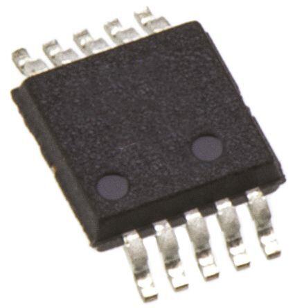
| 描述 | IC DIFF AMP RF/IF LOWDIST 10MSOP差分放大器 Low Distortion RF/IF IC |
| 产品分类 | |
| 品牌 | Analog Devices Inc |
| 产品手册 | |
| 产品图片 |
|
| rohs | 符合RoHS无铅 / 符合限制有害物质指令(RoHS)规范要求 |
| 产品系列 | 放大器 IC,差分放大器,Analog Devices AD8351ARMZ- |
| 数据手册 | |
| P1dB | 13.5dBm |
| 产品型号 | AD8351ARMZ |
| RF类型 | 通用 |
| 产品目录页面 | |
| 产品种类 | 差分放大器 |
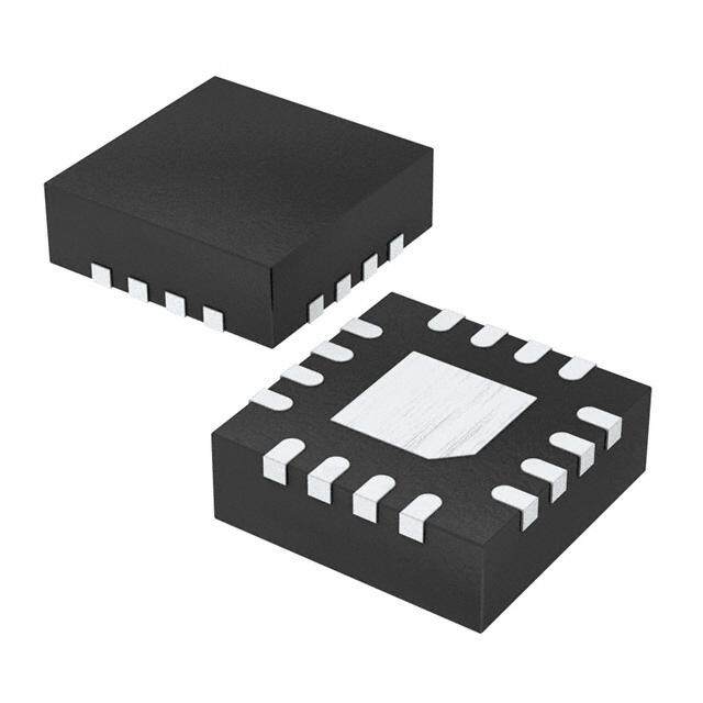
| 供应商器件封装 | 10-MSOP |
| 共模抑制比—最小值 | 43 dB |
| 包装 | 管件 |
| 商标 | Analog Devices |
| 噪声系数 | - |
| 增益 | 26dB |
| 安装风格 | SMD/SMT |
| 封装 | Tube |
| 封装/外壳 | 10-TFSOP,10-MSOP(0.118",3.00mm 宽) |
| 封装/箱体 | MSOP-10 |
| 工作电源电压 | 3 V to 5.5 V |
| 工厂包装数量 | 50 |
| 带宽 | 2.2 GHz |
| 最大功率耗散 | 320 mW |
| 最大工作温度 | + 85 C |
| 最大输入电阻 | 5 kOhms |
| 最小工作温度 | - 40 C |
| 标准包装 | 50 |
| 测试频率 | 10MHz |
| 电压-电源 | 3 V ~ 5.5 V |
| 电流-电源 | 28mA ~ 32mA |
| 电源电流 | 28 mA |
| 稳定时间 | 3 ns |
| 系列 | AD8351 |
| 视频文件 | http://www.digikey.cn/classic/video.aspx?PlayerID=1364138032001&width=640&height=505&videoID=2245193150001 |
| 转换速度 | 13000 V/us |
| 通道数量 | 1 Channel |
| 频率 | 0Hz ~ 2.2GHz |


- 商务部:美国ITC正式对集成电路等产品启动337调查
- 曝三星4nm工艺存在良率问题 高通将骁龙8 Gen1或转产台积电
- 太阳诱电将投资9.5亿元在常州建新厂生产MLCC 预计2023年完工
- 英特尔发布欧洲新工厂建设计划 深化IDM 2.0 战略
- 台积电先进制程称霸业界 有大客户加持明年业绩稳了
- 达到5530亿美元!SIA预计今年全球半导体销售额将创下新高
- 英特尔拟将自动驾驶子公司Mobileye上市 估值或超500亿美元
- 三星加码芯片和SET,合并消费电子和移动部门,撤换高东真等 CEO
- 三星电子宣布重大人事变动 还合并消费电子和移动部门
- 海关总署:前11个月进口集成电路产品价值2.52万亿元 增长14.8%


PDF Datasheet 数据手册内容提取
Low Distortion Differential RF/IF Amplifier Enhanced Product AD8351-EP FEATURES FUNCTIONAL BLOCK DIAGRAM −3 dB bandwidth of 2.2 GHz for A = 12 dB V AD8351-EP Single-resistor programmable gain: 0 dB ≤ AV ≤ 26 dB VOCM PWUP BIAS CELL Differential interface VPOS Low noise input stage: 2.70 nV/√Hz at 70 MHz, A = 10 dB V RGP1 Low harmonic distortion −79 dBc second at 70 MHz INHI OPHI −81 dBc third at 70 MHz INLO OPLO OSiuntgpleu-ts tuhpirpdl-yo ordpeerr aintitoenrc: e3p Vt t(oO I5P.53 )V o f 31 dBm at 70 MHz RGP2 COMM 14821-001 Low power dissipation: 28 mA at 5 V Figure 1. Adjustable output common-mode voltage Fast settling and overdrive recovery Slew rate of 13,000 V/µs Power-down capability ENHANCED PRODUCT FEATURES Supports defense and aerospace applications (AQEC standard) Extended industrial temperature range: −55°C to +105°C Controlled manufacturing baseline 1 assembly/test site 1 fabrication site Product change notification Qualification data available upon request APPLICATIONS Differential ADC drivers Single-ended-to-differential conversion IF sampling receivers RF/IF gain blocks Surface acoustic wave (SAW) filter interfacing GENERAL DESCRIPTION The AD8351-EP is a low cost differential amplifier useful in RF products as in the differential configuration. The exceptionally and IF applications up to 2.2 GHz. The voltage gain can be set good distortion performance makes the AD8351-EP an ideal from unity to 26 dB using a single external gain resistor. The solution for 12-bit and 14-bit IF sampling receiver designs. AD8351-EP provides a nominal 150 Ω differential output Fabricated in the Analog Devices, Inc., high speed XFCB impedance. The excellent distortion performance and low noise process, the AD8351-EP has a high bandwidth that provides characteristics of this device allow a wide range of applications. high frequency performance and low distortion. The quiescent The AD8351-EP is designed to satisfy the demanding current of the AD8351-EP is 28 mA typically. The AD8351-EP performance requirements of communications transceiver amplifier comes in a 16-lead LFCSP package, and operates over applications. The device can be used as a general-purpose gain the temperature range of −55°C to +105°C. block, an ADC driver, and a high speed data interface driver, Additional application and technical information can be found among other functions. The AD8351-EP can also be used as a in the AD8351 datasheet. single-ended-to-differential amplifier with similar distortion Rev. A Document Feedback Information furnished by Analog Devices is believed to be accurate and reliable. However, no responsibility is assumed by Analog Devices for its use, nor for any infringements of patents or other One Technology Way, P.O. Box 9106, Norwood, MA 02062-9106, U.S.A. rights of third parties that may result from its use. Specifications subject to change without notice. No license is granted by implication or otherwise under any patent or patent rights of Analog Devices. Tel: 781.329.4700 ©2016 Analog Devices, Inc. All rights reserved. Trademarks and registered trademarks are the property of their respective owners. Technical Support www.analog.com
AD8351-EP Enhanced Product TABLE OF CONTENTS Features .............................................................................................. 1 Absolute Maximum Ratings ............................................................5 Enhanced Product Features ............................................................ 1 Maximum Power Dissipation ......................................................5 Applications ....................................................................................... 1 ESD Caution...................................................................................5 Functional Block Diagram .............................................................. 1 Pin Configuration and Function Descriptions ..............................6 General Description ......................................................................... 1 Typical Performance Characteristics ..............................................7 Revision History ............................................................................... 2 Outline Dimensions ....................................................................... 12 Specifications ..................................................................................... 3 Ordering Guide .......................................................................... 12 REVISION HISTORY 9/2016—Rev. 0 to Rev. A Change to Quiescent Current Parameter, Table 1 ........................ 3 Changes to Ordering Guide .......................................................... 12 7/2016—Revision 0: Initial Version Rev. A | Page 2 of 12
Enhanced Product AD8351-EP SPECIFICATIONS V = 5 V, R = 150 Ω, R = 110 Ω (A = 10 dB), f = 70 MHz, T = 25°C, parameters specified differentially, unless otherwise noted. The S L G V gain (A ) can be set to any value between 0 dB and 26 dB. V Table 1. Parameter Test Conditions/Comments Min Typ Max Unit DYNAMIC PERFORMANCE −3 dB Bandwidth A = 6 dB, V ≤ 1.0 V p-p 3000 MHz V OUT A = 12 dB, V ≤ 1.0 V p-p 2200 MHz V OUT A = 18 dB, V ≤ 1.0 V p-p 600 MHz V OUT Bandwidth for 0.1 dB Flatness 0 dB ≤ A ≤ 20 dB, V ≤ 1.0 V p-p 200 MHz V OUT Bandwidth for 0.2 dB Flatness 0 dB ≤ A ≤ 20 dB, V ≤ 1.0 V p-p 400 MHz V OUT Gain Accuracy Using 1% resistor for R , 0 dB ≤ A ≤ 20 dB ±1 dB G V Gain Supply Sensitivity V ± 5% 0.08 dB/V S Gain Temperature Sensitivity −55°C to +105°C 3.9 mdB/°C Slew Rate R = 1 kΩ, V = 2 V step 13,000 V/µs L OUT R = 150 Ω, V = 2 V step 7500 V/µs L S Settling Time 1 V step to 1% <3 ns Overdrive Recovery Time V = 4 V to 0 V step, V ≤ ±10 mV <2 ns IN OUT Reverse Isolation (S12) −67 dB INPUT/OUTPUT CHARACTERISTICS Input Common-Mode Voltage Adjustment Range 1.2 to 3.8 V Maximum Output Voltage Swing 1 dB compressed 4.75 V p-p Output Common-Mode Offset 40 mV Output Common-Mode Drift −55°C to +105°C 0.24 mV/°C Output Differential Offset Voltage 20 mV Output Differential Offset Drift −55°C to +105°C 0.13 mV/°C Input Bias Current ±15 µA Input Resistance1 5 kΩ Input Capacitance1 0.8 pF Common-Mode Rejection Ratio (CMRR) 43 dB Output Resistance1 150 Ω Output Capacitance1 0.8 pF POWER INTERFACE Supply Voltage 3 5.5 V PWUP Threshold 1.3 V PWUP Input Bias Current PWUP at 5 V 100 µA PWUP at 0 V 25 µA Quiescent Current −55°C to +105°C 28 35 mA NOISE/DISTORTION 10 MHz Second/Third Harmonic Distortion2 R = 1 kΩ, V = 2 V p-p −95/−93 dBc L OUT R = 150 Ω, V = 2 V p-p −80/−69 dBc L OUT Third-Order Intermodulation Distortion (IMD) R = 1 kΩ, f1 = 9.5 MHz, f2 = 10.5 MHz, −90 dBc L V = 2 V p-p composite OUT R = 150 Ω, f1 = 9.5 MHz, f2 = 10.5 MHz, −70 dBc L V = 2 V p-p composite OUT Output Third-Order Intercept f1 = 9.5 MHz, f2 = 10.5 MHz 33 dBm Noise Spectral Density (Referred to Input (RTI)) 2.65 nV/√Hz 1 dB Compression Point 13.5 dBm Rev. A | Page 3 of 12
AD8351-EP Enhanced Product Parameter Test Conditions/Comments Min Typ Max Unit 70 MHz Second/Third Harmonic Distortion2 R = 1 kΩ, V = 2 V p-p −79/−81 dBc L OUT R = 150 Ω, V = 2 V p-p −65/−66 dBc L OUT Third-Order IMD R = 1 kΩ, f1 = 69.5 MHz, f2 = 70.5 MHz, −85 dBc L V = 2 V p-p composite OUT R = 150 Ω, f1 = 69.5 MHz, f2 = 70.5 MHz, −69 dBc L V = 2 V p-p composite OUT Output Third-Order Intercept f1 = 69.5 MHz, f2 = 70.5 MHz 31 dBm Noise Spectral Density (RTI) 2.70 nV/√Hz 1 dB Compression Point 13.3 dBm 140 MHz Second/Third Harmonic Distortion2 R = 1 kΩ, V = 2 V p-p −69/−69 dBc L OUT R = 150 Ω, V = 2 V p-p −54/−53 dBc L OUT Third-Order IMD R = 1 kΩ, f1 = 139.5 MHz, f2 = 140.5 MHz, −79 dBc L V = 2 V p-p composite OUT R = 150 Ω, f1 = 139.5 MHz, f2 = 140.5 MHz, −67 dBc L V = 2 V p-p composite OUT Output Third-Order Intercept f1 = 139.5 MHz, f2 = 140.5 MHz 29 dBm Noise Spectral Density (RTI) 2.75 nV/√Hz 1 dB Compression Point 13 dBm 240 MHz Second/Third Harmonic Distortion2 R = 1 kΩ, V = 2 V p-p −60/−66 dBc L OUT R = 150 Ω, V = 2 V p-p −46/−50 dBc L OUT Third-Order IMD R = 1 kΩ, f1 = 239.5 MHz, f2 = 240.5 MHz, −76 dBc L V = 2 V p-p composite OUT R = 150 Ω, f1 = 239.5 MHz, f2 = 240.5 MHz, −62 dBc L V = 2 V p-p composite OUT Output Third-Order Intercept f1 = 239.5 MHz, f2 = 240.5 MHz 27 dBm Noise Spectral Density (RTI) 2.90 nV/√Hz 1 dB Compression Point 13 dBm 1 Values are specified differentially. 2 See the AD8351 data sheet for information about single-ended to differential operation. Rev. A | Page 4 of 12
Enhanced Product AD8351-EP ABSOLUTE MAXIMUM RATINGS MAXIMUM POWER DISSIPATION Table 2. The maximum power that can be safely dissipated by this device Parameter Rating is limited by the associated rise in junction temperature. Supply Voltage, VPOS 6 V Exceeding a junction temperature of 125°C for an extended PWUP Voltage VPOS period can result in device failure. Internal Power Dissipation 320 mW θ 79.1°C/W To ensure proper operation of the AD8351-EP, it is necessary to JA Maximum Junction Temperature 125°C observe the maximum power derating curve (see Figure 2) to Operating Temperature Range −55°C to +105°C guarantee that the maximum junction temperature (125°C) is Storage Temperature Range −65°C to +150°C not exceeded under all conditions. Lead Temperature Range (Soldering, 60 sec) 300°C 0.350 Stresses at or above those listed under Absolute Maximum W)0.325 Ratings may cause permanent damage to the product. This is a N ( O stress rating only; functional operation of the product at these TI or any other conditions above those indicated in the operational SIPA0.300 S section of this specification is not implied. Operation beyond DI R 0.275 the maximum operating conditions for extended periods may E W affect product reliability. PO M 0.250 U M XI A M0.225 0.200 –60 –50 –40 –30 –20AM–10BIE0NT10 TEM20PE30RAT40UR50E (°60C) 70 80 90 100 11014821-002 Figure 2. Maximum Power Dissipation vs. Temperature ESD CAUTION Rev. A | Page 5 of 12
AD8351-EP Enhanced Product PIN CONFIGURATION AND FUNCTION DESCRIPTIONS P M U C W C C O P N N V 6 5 4 3 1 1 1 1 RGP1 1 12 VPOS INHI 2 AD8351-EP 11 OPHI INLO 3 TOP VIEW 10 OPLO (Not to Scale) RGP2 4 9 COMM 5 6 7 8 C C C C N N N N NOTES 1.NC = NO CONNECT. DO NOT CONNECT TO THIS PIN. 2.TGIMHNPEDE EDAXANPNDOC MSEUE GDSRT PO BAUEDN SIDSO PILNLDTAEENRREEN.DA LTLOY A C LOONWNECTED TO 14821-003 Figure 3. Pin Configuration Table 3. Pin Function Descriptions Pin No. Mnemonic Description 1 RGP1 Gain Resistor Input 1. 2 INHI Balanced Differential Input, High. Biased to midsupply, typically ac-coupled. 3 INLO Balanced Differential Input, Low. Biased to midsupply, typically ac-coupled. 4 RGP2 Gain Resistor Input 2. 5, 6, 7, 8, 14, 15 NC No Connect. Do not connect to this pin. 9 COMM Device Common. Connect this pin to a low impedance ground. 10 OPLO Balanced Differential Output, Low. Biased to VOCM, typically ac-coupled. 11 OPHI Balanced Differential Output, High. Biased to VOCM, typically ac-coupled. 12 VPOS Positive Supply Voltage. 3 V to 5.5 V. 13 VOCM Input/Output Common-Mode Voltage. The voltage applied to this pin sets the common-mode voltage at both the input and output. This pin is typically decoupled to ground with a 0.1 µF capacitor. 16 PWUP Apply a positive voltage (1.3 V ≤ V ≤ VPOS) to activate the device. PWUP EPAD Exposed Pad. The exposed pad is internally connected to GND and must be soldered to a low impedance ground plane. Rev. A | Page 6 of 12
Enhanced Product AD8351-EP TYPICAL PERFORMANCE CHARACTERISTICS V = 5 V, T = 25°C, unless otherwise noted. S 20 30 RG = 20Ω RG = 10Ω 25 15 RG = 80Ω 20 dB) 10 dB) RG = 50Ω AIN ( RG = 200Ω AIN ( 15 G 5 G 10 RG = 200Ω 0 5 –5 0 1 10 FREQUE1N0C0Y (MHz) 1000 10000 14821-103 1 10 FREQUE1N0C0Y (MHz) 1000 10000 14821-006 Figure 4. Gain vs. Frequency for a 150 Ω Differential Load Figure 7. Gain vs. Frequency for a 1 kΩ Differential Load (AV = 6 dB, 12 dB, and 18 dB) (AV = 10 dB, 18 dB, and 26 dB) 35 1.0 0.9 30 0.8 0.7 0.6 25 0.5 20 dB) 00..34 N (dB) 15 TNESS ( 00..210 RL = 150Ω GAI 105 RL = OPEN AIN FLA–––000...231 RL = 1kΩ RL = 150Ω G––00..45 0 –0.6 –0.7 –5 RL = 1kΩ –0.8 –0.9 –10 –1.0 10 100 RG (Ω) 1k 10k 14821-004 1 10FREQUENCY (MHz1)00 1000 14821-007 Figure 5. Gain vs. Gain Resistor, RG (f = 100 MHz, Figure 8. Gain Flatness vs. Frequency RL = 150 Ω, 1 kΩ, and Open) (RL = 150 Ω and 1 kΩ, AV = 10 dB) 10.75 10.50 0 –10 10.50 10.25 –20 Ω (dB)10.25 10.00 Ω (dB) dB)–30 GAIN; R = 1kL109..0705 99..5705 GAIN; R = 150L ISOLATION (–––654000 –70 9.50 9.25 –80 9.25 9.00 –60 –40 –20 0TEMP2E0RATU4R0E (°C6)0 80 100 120 14821-005 –900 100 200 300 FR4E00QUE5N00CY (6M0H0z) 700 800 900 1000 14821-008 Figure 6. Gain vs. Temperature at 100 MHz (AV = 10 dB) Figure 9. Isolation vs. Frequency (AV = 10 dB) Rev. A | Page 7 of 12
AD8351-EP Enhanced Product –30 –45 –50 SINGLE-ENDED INPUT Bc) Bc) –55 d –40 HD3 –55 d OS = 5V ( –50 –65 OS = 3V ( N (dBc) ––6605 P HD2 P O ON; V –60 HD2 –75 ON; V ORTI –70 DISTORTI –70 HD3 –85 DISTORTI ONIC DIST ––7850 HD2 C –80 –95 C M –85 HD3 MONI DIFFERENTIAL INPUT MONI HAR –90 R –90 –105 R A A H H –95 –1000 25 50 75 FR1E00QUE1N2C5Y (1M5H0z) 175 200 225 250–115 14821-009 –1000 10 20 30 FR4E0QUE5N0CY (M60Hz) 70 80 90 100 14821-012 Figure 10. Harmo(nAicV =D i1st0o drtBio, ant v3s .V F arenqdu 5e nVc Syu fpopr l2ie Vs) p -p into RL = 1 kΩ Figure 13. Harmonic DSisitnogrlteio-Enn vdse. dF rIenqpuuetn (AcyV =fo 1r 02 dVB p)- p into RL = 1 kΩ Using 0 –20 –50 dBc) –10 HD3 –30 dBc) –55 SINGLE-ENDED INPUT V ( V ( POS = 5 ––3200 ––5400 POS = 3 N (dBc) ––6605 ON; V –40 HD2 –60 ON; V RTIO –70 HD3 C DISTORTI ––6500 HD3 ––8700 C DISTORTI ONIC DISTO ––7850 HD2 ONI –70 DIFFERENTIAL INPUT –90 ONI RM –85 M M A R R H –90 A –80 HD2 –100 A H H –95 –900 25 50 75 FR1E00QUE1N2C5Y (1M5H0z) 175 200 225 250–110 14821-010 –1000 10 20 30 FR4E0QUE5N0CY (M60Hz) 70 80 90 100 14821-013 Figure 11. Harmonic Distortion vs. Frequency for 2 V p-p into RL = 150 Ω Figure 14. Harmonic Distortion vs. Frequency for 2 V p-p into RL = 150 Ω (AV = 10 dB) Using Single-Ended Input (AV = 10 dB) 3.00 3.00 NOISE SPECTRAL DENSITY (nV/√Hz) 22222222........6677889905050505 NOISE SPECTRAL DENSITY (nV/√Hz) 22222222........6677889905050505 2.55 2.55 2.500 50 FR1E00QUENCY (1M5H0z) 200 250 14821-011 2.500 50 FR1E00QUENCY (1M5H0z) 200 250 14821-014 Figure 12. Noise Spectral Density (RTI) vs. Frequency Figure 15. Noise Spectral Density (RTI) vs. Frequency (RL = 150 Ω, 5 V Supply, AV = 10 dB) (RL = 150 Ω, 3 V Supply, AV = 10 dB) Rev. A | Page 8 of 12
Enhanced Product AD8351-EP 16 –70 14 m) B –75 ESSION (d 1120 VRRPLL O== S11 5k=0Ω 5ΩV MD (dBc) –80 PR R I M 8 E CO RL = 150Ω RD 1dB 6 VRPL O= S1 k=Ω 3V RD-O –85 PUT 4 THI UT –90 O 2 0 –95 0 25 50 75 FR1E00QUE1N2C5Y (1M5H0z) 175 200 225 250 14821-015 0 25 50 75 FR1E00QUE1N2C5Y (1M5H0z) 175 200 225 250 14821-018 Figure 16. Output 1 dB Compression (P1dB) vs. Frequency Figure 19. Third-Order Intermodulation Distortion (IMD) vs. Frequency for a 2 (RL = 150 Ω and 1 kΩ, AV = 10 dB, at 3 V and 5 V Supplies) V p-p Composite Signal into RL = 1 kΩ (AV = 10 dB, at 5 V Supplies) 16 –50 14 VPOS = 5V m) B –55 ESSION (d 1120 MD (dBc) –60 PR R I OM 8 VPOS = 3V DE C R dB 6 D-O –65 1 R PUT 4 THI UT –70 O 2 0 –75 10 GAIN RE1S0I0STOR (Ω) 1000 14821-016 0 25 50 75 FR1E00QUE1N2C5Y (1M5H0z) 175 200 225 250 14821-019 Figure 17. Output 1 dB Compression (P1dB) vs. Gain Resistor (RG) Figure 20. Third-Order Intermodulation Distortion vs. Frequency for a 2 V p-p (f =100, RL = 150 Ω, AV = 10 dB, at 3 V and 5 V Supplies) Composite Signal into RL = 150 Ω (AV = 10 dB, at 5 V Supplies) 13.29 13.30 13.31 O13.32UTPU13.33T 1d13.34B CO13.35MPR13.36ESSI13.37ON (13.38dB) 13.39 13.40 13.41 14821-017 –68.T0H–IR68D.2-O–R68D.4ER– 6I8N.6TE–R68M.8OD–6U9L.0AT–6IO9.N2 D–6IS9.T4O–R69T.I6ON–6 9(d.8Bc–)70.0 14821-020 Figure 18. Output Compression Point Distribution Figure 21. Third-Order Intermodulation Distortion Distribution (f = 70 MHz, RL = 150 Ω, AV = 10 dB) (f = 70 MHz, RL = 150 Ω, AV = 10 dB) Rev. A | Page 9 of 12
AD8351-EP Enhanced Product 4000 0 3500 Ω) 3000 –25 E ( D DANCE MAGNITU 221505000000 –50 PHASE (Degrees) 3GHz 10MHz 10MHz E MP 1000 –75 500MHz I 3GHz WITH 50Ω 500MHz 500 TERMINATIONS 0 –100 WITHOUT 10 FREQUE1N0C0Y (MHz) 1000 14821-021 TERMINATIONS 14821-024 Figure 22. Input Impedance vs. Frequency Figure 25. Input Reflection Coefficient vs. Frequency (RS = RL = 100 Ω With and Without 50 Ω Terminations) 160 30 150 25 UDE (Ω) 140 20 Degrees) NIT E ( MPEDANCE MAG 113200 1150 MPEDANCE PHAS 105M00HMzHz I 110 5 I 100 0 3GHz 10 FREQUE1N0C0Y (MHz) 1000 14821-022 14821-025 Figure 23. Output Impedance Magnitude and Phase vs. Frequency Figure 26. Output Reflection Coefficient vs. Frequency (RS = RL = 100 Ω) 0 20 19 –2 18 17 –4 16 15 grees) ––68 111234 AY (ps) De 11 EL PHASE ( ––1102 78910 GROUP D 6 –14 5 4 –16 3 1 –18 0 0 25 50 75 FR1E00QUE1N2C5Y (1M5H0z) 175 200 225 250 14821-023 Figure 24. Phase and Group Delay (AV = 10 dB, at 5 V Supplies) Rev. A | Page 10 of 12
Enhanced Product AD8351-EP 80 3 VOUT 70 2 RL = 150Ω 60 1 dB) E (V) VIN RR ( 50 RL = 1kΩ TAG 0 M L C O V 40 –1 30 –2 201 10FREQUENCY (MHz1)00 1000 14821-026 –30 5 10 15 20TIM2E5 (ns)30 35 40 45 50 14821-029 Figure 27. Common-Mode Rejection Ratio, CMRR (RS = 100 Ω) Figure 30. Overdrive Recovery Using Sinusoidal Input Waveform RL = 150 Ω (AV = 10 dB, at 5 V Supplies) 0.6 1.00 0pF 0.75 0.4 5pF 2pF 0.50 10pF 0.2 V) V) 0.25 E ( E ( G G A 0 A 0 T T L L O O V V–0.25 –0.2 –0.50 –0.4 –0.75 –0.615 16 17 18 19TIM2E0 (ns)21 22 23 24 25 14821-027 –1.000 0.5 1.0 1.5 TIM2E.0 (ns) 2.5 3.0 3.5 4.0 14821-030 Figure 28. Transient Response Under Capacitive Loading Figure 31. Large Signal Transient Response for a 1 V p-p Output Step (RL = 150 Ω, CL = 0 pF, 2 pF, 5 pF, 10 pF) (AV = 10 dB, RIP = 25 Ω) 5.0 5 4.5 4 4.0 3 3.5 2 PUT (V) 32..05 LING (%) 01 T T U T O 2.0 E –1 S 1.5 –2 1.0 –3 0.5 –4 00 5 10 15 TIM2E0 (ns) 25 30 35 40 14821-028 –50 3 6TIME (ns)9 12 15 14821-031 Figure 29. 2× Output Overdrive Recovery (RL = 150 Ω, AV = 10 dB) Figure 32. 1% Settling Time for a 2 V p-p Step (AV = 10 dB, RL = 150 Ω) Rev. A | Page 11 of 12
AD8351-EP Enhanced Product OUTLINE DIMENSIONS 3.10 0.30 3.00 SQ 0.25 PIN 1 2.90 0.18 PIN 1 INDICATOR INDICATOR 0.50 13 16 (0.30) BSC 12 1 1.80 EXPPAODSED 1.70 SQ 1.60 9 4 *0.45 8 5 0.20 MIN TOP VIEW 0.40 BOTTOM VIEW 0.30 0.80 FOR PROPER CONNECTION OF 0.75 0.05 MAX THE EXPOSED PAD, REFER TO 0.70 THE PIN CONFIGURATION AND 0.02 NOM FUNCTION DESCRIPTIONS COPLANARITY SECTION OF THIS DATA SHEET. PKG-004087/PKG-005014 SEPALTAINNGE *CWOITMHP LEIXACNETP TTOIO JNE TD0OE.2 CL0 E3S ATRDAE NFLDEANR0G.D0H8ST .MO-220-WEED-4 10-22-2015-B Figure 33. 16-Lead Lead Frame Chip Scale Package [LFCSP] 3 mm × 3 mm Body and 0.75 mm Package Height (CP-16-33) Dimensions shown in millimeters ORDERING GUIDE Model1 Temperature Range Package Description Package Option Branding AD8351SCPZ-EP-R7 −55°C to +105°C 16-Lead Lead Frame Chip Scale Package [LFCSP] CP-16-33 Q26 1 Z = RoHS Compliant Part. ©2016 Analog Devices, Inc. All rights reserved. Trademarks and registered trademarks are the property of their respective owners. D14821-0-9/16(A) Rev. A | Page 12 of 12
Mouser Electronics Authorized Distributor Click to View Pricing, Inventory, Delivery & Lifecycle Information: A nalog Devices Inc.: AD8351ARM AD8351ARMZ AD8351ARM-REEL7 AD8351ARMZ-REEL7 AD8351ACPZ-R7 AD8351-EVALZ AD8351SCPZ-EP-R7