ICGOO在线商城 > 射频/IF 和 RFID > RF 放大器 > MWIC930NR1
 Datasheet下载
- 型号: MWIC930NR1
- 制造商: Freescale Semiconductor
- 库位|库存: xxxx|xxxx
- 要求:
| 数量阶梯 | 香港交货 | 国内含税 |
| +xxxx | $xxxx | ¥xxxx |
查看当月历史价格
查看今年历史价格
MWIC930NR1产品简介:
ICGOO电子元器件商城为您提供MWIC930NR1由Freescale Semiconductor设计生产,在icgoo商城现货销售,并且可以通过原厂、代理商等渠道进行代购。 MWIC930NR1价格参考。Freescale SemiconductorMWIC930NR1封装/规格:RF 放大器, 射频放大器 IC 手机,GSM,EDGE,N-CDMA 900MHz TO-272 WB-16。您可以下载MWIC930NR1参考资料、Datasheet数据手册功能说明书,资料中有MWIC930NR1 详细功能的应用电路图电压和使用方法及教程。
NXP USA Inc.的MWIC930NR1是一款射频(RF)放大器,主要应用于无线通信系统中。该器件是一款高性能的射频功率放大器,适用于蜂窝通信基础设施,如基站和中继站。其主要应用场景包括:

1. 蜂窝通信系统:MWIC930NR1广泛用于2G、3G、4G LTE等移动通信网络中的基站设备,用于增强上行和下行信号的功率,确保信号覆盖范围和通信质量。

2. 无线基础设施:该放大器适用于宏基站、微基站和射频拉远单元(RRU),在分布式天线系统(DAS)中也常用于提升信号强度和传输效率。

3. 工业与商业通信设备:除了公共移动网络,MWIC930NR1也可用于专网通信系统,如电力、交通、安防等行业的无线调度通信系统。

4. 测试与测量设备:在射频测试系统中,该器件可用于模拟真实工作环境下的功率输出,评估系统性能。

该放大器具有高线性度、高效率和良好的热稳定性,适合在复杂电磁环境中稳定工作。其封装设计便于散热,适用于高密度电路布局。

总之,MWIC930NR1是一款适用于多种无线通信基础设施的高性能射频功率放大器,能够有效提升信号传输距离和系统整体性能。
| 参数 | 数值 |
| 产品目录 | |
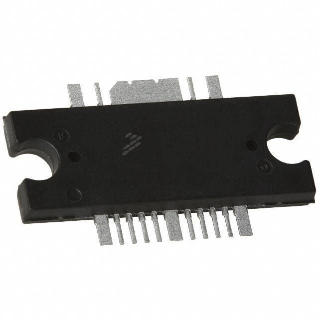
| 描述 | IC PWR AMP RF 30W TO272-16 |
| 产品分类 | |
| 品牌 | Freescale Semiconductor |
| 数据手册 | |
| 产品图片 |
|
| P1dB | - |
| 产品型号 | MWIC930NR1 |
| RF类型 | 手机,GSM,EDGE,N-CDMA |
| rohs | 含铅 / 符合限制有害物质指令(RoHS)规范要求 |
| 产品系列 | - |
| 产品目录页面 | |
| 供应商器件封装 | TO-272 WB-16 |
| 其它名称 | MWIC930NR1TR |
| 包装 | 带卷 (TR) |
| 噪声系数 | - |
| 增益 | 30dB |
| 封装/外壳 | TO-272-16 变式, 扁平引线 |
| 标准包装 | 500 |
| 测试频率 | - |
| 电压-电源 | 26V |
| 电流-电源 | 90mA |
| 频率 | 900MHz |


- 商务部:美国ITC正式对集成电路等产品启动337调查
- 曝三星4nm工艺存在良率问题 高通将骁龙8 Gen1或转产台积电
- 太阳诱电将投资9.5亿元在常州建新厂生产MLCC 预计2023年完工
- 英特尔发布欧洲新工厂建设计划 深化IDM 2.0 战略
- 台积电先进制程称霸业界 有大客户加持明年业绩稳了
- 达到5530亿美元!SIA预计今年全球半导体销售额将创下新高
- 英特尔拟将自动驾驶子公司Mobileye上市 估值或超500亿美元
- 三星加码芯片和SET,合并消费电子和移动部门,撤换高东真等 CEO
- 三星电子宣布重大人事变动 还合并消费电子和移动部门
- 海关总署:前11个月进口集成电路产品价值2.52万亿元 增长14.8%


PDF Datasheet 数据手册内容提取
Freescale Semiconductor Document Number: MWIC930 Technical Data Replaced by MWIC930NR1(GNR1). There are no form, fit or function changes with this part Rev. 5, 5/2006 replacement. N suffix added to part number to indicate transition to lead-free terminations. RF LDMOS Wideband Integrated Power Amplifiers MWIC930R1 The MWIC930 wideband integrated circuit is designed for CDMA and MWIC930GR1 GSM/GSM EDGE applications. It uses Freescale(cid:146)s newest High Voltage (26 to 28 Volts) LDMOS IC technology and integrates a multi-stage structure. Its wideband On-Chip integral matching circuitry makes it usable from 790 to 1000 MHz. The linearity performances cover all modulations for cellular applications: GSM, GSM EDGE, TDMA, N-CDMA and W-CDMA. 746-960 MHz, 30 W, 26-28 V Final Application SINGLE N-CDMA, GSM/GSM EDGE • Typical Performance @ P1dB: V = 26 Volts, I = 90 mA, I = RF LDMOS WIDEBAND INTEGRATED DD DQ1 DQ2 240 mA, Pout = 30 Watts P1dB, Full Frequency Band (921-960 MHz) POWER AMPLIFIERS Power Gain (cid:151) 30 dB N Power Added Efficiency (cid:151) 45% N Driver Application O O • Typical Single-Carrier N-CDMA Performance: V = 27 Volts, I = DD DQ1 90 mA, I = 240 mA, P = 5 Watts Avg., Full Frequency Band I DQ2 out I T (865-894 MHz), IS -95 (Pilot, Sync, Paging, Traffic Codes 8 Through 13), T Channel Bandwidth = 1.2288 MHz. PAR = 9.8 dB @ 0.01% A Probability on CCDF. A Power Gain (cid:151) 31 dB CASE 1329-09 M Power Added Efficiency (cid:151) 21% TO-272 WB-16 M ACPR @ 750 kHz Offset (cid:151) -52 dBc in 30 kHz Bandwidth PLASTIC R• Capable of Handling 5:1 VSWR, @ 26 Vdc, 921 MHz, 30 Watts CW Output MWIC930R1 R Power O• Characterized with Series Equivalent Large-Signal Impedance Parameters O • On-Chip Matching (50 Ohm Input, DC Blocked, >4 Ohm Output) F• Integrated Quiescent Current Temperature Compensation with F N Enable/Disable Function N • On-Chip Current Mirror gm Reference FET for Self Biasing Application (1) CASE 1329A-03 I• Integrated ESD Protection TO-272 WB-16 GULL I E• 200°C Capable Plastic Package PLASTIC E • In Tape and Reel. R1 Suffix = 500 Units per 44 mm, 13 inch Reel. MWIC930GR1 V V I I H H V C RD2 GND 1 16 GND C R VRG2 VVRRGD22 23 15 NC R V VDS1 4 A DS1 VRD1 5 A RF RFin 6 14 V out/ RF V /RF DS2 in DS2 out VRG1 7 VGS1 8 VRD1 VGS2 9 V NC 10 13 NC RG1 GND 11 12 GND V (Top View) GS1 Quiescent Current VGS2 Temperature Compensation Note: Exposed backside flag is source terminal for transistors. Figure 1. Functional Block Diagram Figure 2. Pin Connections 1. Refer to AN1987/D, Quiescent Current Control for the RF Integrated Circuit Device Family. Go to http://www.freescale.com/rf. Select Documentation/Application Notes - AN1987. © Freescale Semiconductor, Inc., 2006. All rights reserved. MWIC930R1 MWIC930GR1 RF Device Data Freescale Semiconductor 1
Table 1. Maximum Ratings Rating Symbol Value Unit Drain-Source Voltage VDSS -0.5, +65 Vdc Gate-Source Voltage VGS -0.5, +15 Vdc Storage Temperature Range Tstg -65 to +175 °C Operating Junction Temperature TJ 200 °C Table 2. Thermal Characteristics Characteristic Symbol Value (1,2) Unit Thermal Resistance, Junction to Case RθJC °C/W GSM Application Stage 1, 26 Vdc, IDQ = 90 mA 5.9 (Pout = 30 W CW) Stage 2, 26 Vdc, IDQ = 240 mA 1.4 GSM EDGE Application Stage 1, 27 Vdc, IDQ = 90 mA 6.5 N (Pout = 15 W CW) Stage 2, 27 Vdc, IDQ = 240 mA 1.7 N O CDMA Application Stage 1, 27 Vdc, IDQ = 90 mA 6.5 O (Pout = 5 W CW) Stage 2, 27 Vdc, IDQ = 240 mA 1.8 I I TTable 3. ESD Protection Characteristics T A Test Conditions Class A Human Body Model 1 (Minimum) M M Machine Model M3 (Minimum) R Charge Device Model C2 (Minimum) R Table 4. Moisture Sensitivity Level O O Test Methodology Rating Package Peak Temperature Unit F F Per JESD 22-A113, IPC/JEDEC J-STD-020 3 260 °C N N Table 5. Electrical Characteristics (TC = 25°C, unless otherwise noted) I Characteristic Symbol Min Typ Max Unit I EFunctional Tests (In Freescale Test Fixture, 50 ohm system) VDD = 27 Vdc, IDQ1 = 90 mA, IDQ2 = 240 mA, Pout = 5 W Avg. N-CDMA, E f = 880 MHz, Single-Carrier N-CDMA, 1.2288 MHz Channel Bandwidth Carrier. ACPR measured in 30 kHz Bandwidth @ ±750 MHz Offset. VPAR = 9.8 dB @ 0.01% Probability on CCDF V I Power Gain Gps 28 31 (cid:151) dB I H H Power Added Efficiency PAE 18 21 (cid:151) % C Input Return Loss IRL (cid:151) -12 -9 dB C (f = 880 MHz) R R Adjacent Channel Power Ratio ACPR (cid:151) -52 -48 dBc ATypical Performances (In Freescale Test Fixture) VDD = 26 Vdc, IDQ1 = 90 mA, IDQ2 = 240 mA, 840 MHz<Frequency<920 MHz A Quiescent Current Accuracy over Temperature (2) (cid:151) (cid:151) % Stage 1 with 33.2 kΩ Gate Feed Resistors (-30 to 115°C) ΔI1QT ±2.5 Stage 2 with 47.5 kΩ Gate Feed Resistors (-30 to 115°C) ΔI2QT ±2.5 Gain Flatness in 80 MHz Bandwidth @ Pout = 5 W CW GF (cid:151) 0.3 (cid:151) dB Deviation from Linear Phase in 80 MHz Bandwidth @ Pout = 5 W CW Φ (cid:151) 0.6 (cid:151) ° Delay @ Pout = 5 W CW Including Output Matching Delay (cid:151) 3 (cid:151) ns Part-to-Part Phase Variation @ Pout = 5 W CW ΔΦ (cid:151) ±15 (cid:151) ° 1. Refer to AN1955/D, Thermal Measurement Methodology of RF Power Amplifiers. Go to http://www.freescale.com/rf. Select Documentation/Application Notes - AN1955. 2. Refer to AN1977/D, Quiescent Current Thermal Tracking Circuit in the RF Integrated Circuit Family. Go to http://www.freescale.com/rf. Select Documentation/Application Notes - AN1977. (continued) MWIC930R1 MWIC930GR1 RF Device Data 2 Freescale Semiconductor
Table 5. Electrical Characteristics (TC = 25°C, unless otherwise noted) (continued) Characteristic Symbol Min Typ Max Unit Typical GSM/GSM EDGE Performances (In Freescale GSM/GSM EDGE Test Fixture, 50 οhm system) VDD = 27 Vdc, IDQ1 = 90 mA, IDQ2 = 240 mA, 921 MHz<Frequency<960 MHz Output Power, 1dB Compression Point P1dB (cid:151) 30 (cid:151) W Power Gain @ Pout = 30 W CW Gps (cid:151) 30 (cid:151) dB Power Added Efficiency @ Pout = 30 W CW PAE (cid:151) 45 (cid:151) % Input Return Loss @ Pout = 30 W CW IRL (cid:151) -12 (cid:151) dB Intermodulation Distortion IMD (cid:151) -30 (cid:151) dBc (15 W, 2-Tone, 100 kHz Tone Spacing) Intermodulation Distortion IMD (cid:151) -45 (cid:151) dBc (1 W, 2-Tone, 100 kHz Tone Spacing) backoff Gain Flatness in a 40 MHz Bandwidth @ Pout = 30 W CW GF (cid:151) 0.3 (cid:151) dB N Deviation from Linear Phase in a 40 MHz Bandwidth @ Pout = 30 W CW Φ (cid:151) 0.6 (cid:151) ° N O O I I T T A A M M R R O O F F N N I I E E V V I I H H C C R R A A MWIC930R1 MWIC930GR1 RF Device Data Freescale Semiconductor 3
Z8 V 1 16 VD2 D1 C5 C6 C15 C12 C9 2 NC 15 3 Z7 RF 4 RF INPUT 5 OUTPUT Z1 Z2 Z3 Z4 Z5 C3 Z6 14 6 C1 C2 7 Z9 V 8 G1 9 R1 C13 R3 C10 C7 10 NC Quiescent Current NC 13 C4 Temperature Compensation 11 12 V G2 Z10 R2 C14 R4 C11 C8 N N O O Z1 0.0438″ x 0.970″50 Ω Microstrip Z6 0.0438″ x 0.2009″Microstrip I (not including lead pad) Z7 0.5274″ x 0.0504″Microstrip I T Z2 0.234″ x 0.1183″Microstrip Z8 0.0504″ x 0.250″Microstrip T (including lead pad) Z9 0.880″ x 0.0254″Microstrip A A Z3 0.1575″ x 0.9379″Microstrip Z10 0.0254″ x 0.250″Microstrip M Z4 0.08425″ x 0.0729″Microstrip PCB Rogers 4350, 0.020″, εr = 3.50 M Z5 0.08425″ x 0.5111″Microstrip R Figure 3. MWIC930R1(GR1) Test Fixture Schematic R O O Table 6. MWIC930R1(GR1) Test Fixture Component Designations and Values F F Part Description Part Number Manufacturer N *C1 15 pF High Q Capacitor ATC600S150JW ATC N *C2 6.8 pF High Q Capacitor - GSM Fixture ATC600S6R8CW ATC I 8.2 pF High Q Capacitor - CDMA Fixture ATC600S8R2CW I E *C3 5.6 pF High Q Capacitor ATC600S5R6CW ATC E *C4, C5, C7, C8, C9 47 pF High Q Capacitors ATC600S470JW ATC V V C6, C13, C14, C15 1 μF Chip Capacitors GRM42-2X7R105K050AL Murata I C10, C11, C12 10 nF Chip Capacitors C0603C103J5R Kemet I H H R1, R2 1 k(cid:2), 1/8 W Chip Resistors RM73B2AT102J KOA Speer C R3, R4 1 M(cid:2), 1/4 W Chip Resistors RM73B2BT105J KOA Speer C *For output matching and bypass purposes, it is strongly recommended to use these exact capacitors. R R A A MWIC930R1 MWIC930GR1 RF Device Data 4 Freescale Semiconductor
VD1 C15 MWIC930 Rev 0 VD2 C6 N N C5 O O I I T C12 T A A RF RF M Input C9 C3 Output M R C7 C1 C2 R O C10 C8 O R3 C11 F F N C13 N C4 I R1 I E E VG1 V V I I H H R4 C C R R A C14 R2 A VG2 Freescale has begun the transition of marking Printed Circuit Boards (PCBs) with the Freescale Semiconductor signature/logo. PCBs may have either Motorola or Freescale markings during the transition period. These changes will have no impact on form, fit or function of the current product. Figure 4. MWIC930R1(GR1) Test Circuit Component Layout MWIC930R1 MWIC930GR1 RF Device Data Freescale Semiconductor 5
TYPICAL CHARACTERISTICS −20 34 N (dBc) −25 VPDouDt == 1257 WVd (cAvg.) 33 TC = −30(cid:2)C ORTIO −30 IIDDQQ12 == 29400 m mAA N (dB) 32 25(cid:2)C ST f = 880 MHz AI LATION DI −−3450 Two−Tone PEP = 30 W 3rd Order POWER G 3310 85(cid:2)C DU 5th Order , s O p M −45 G 29 V = 27 Vdc R DD E I = 90 mA T DQ1 INMD, −50 7th Order 28 If D=Q 82 8=0 2M4H0 zmA I −55 27 0.1 1 10 100 0 5 10 15 20 25 30 35 40 N N TONE SPACING (MHz) P , OUTPUT POWER (WATTS) out O Figure 5. Intermodulation Distortion Products Figure 6. Power Gain versus Output Power O versus Output Power I I T T A 32 40 A M Pin = 0 dBm 38 M 30 36 B) d RdB) 28 AIN ( 34 TC = −30(cid:2)C R INFOG, POWER GAIN (ps 222642 91 2d BdBmm 6 dBm 3 dBm IDQ1 = 90 mA G, POWER Gps 3322220864 2855(cid:2)(cid:2)CC VPDouDt == 3207 WVd (cCW) INFO E 15 dBm If D=Q 82 8=0 2M4H0 zmA 22 IIDQ1 == 29400 m mAA E 20 20 DQ2 V 5 10 15 20 25 30 35 700 750 800 850 900 950 1000 V V , SUPPLY VOLTAGE (VOLTS) f, FREQUENCY (MHz) DD I I H Figure 7. Power Gain versus Supply Voltage Figure 8. Power Gain versus Frequency H C C R −16 c) −40 R B AdB) −18 VIIDDDQQD12 === 229740 0 Vm mdAcA RATIO (d −−4424 VIIDDDQQD12 === 229740 0 Vm mdAcA TC = 85(cid:2)C A OSS ( −20 f = 880 MHz TC = 85(cid:2)C WER −46 f9 =−C 8h8a0n MneHl zIS−95 CDMA N L PO −48 TUR −22 NEL −50 25(cid:2)C UT RE 25(cid:2)C CHAN −52 −30(cid:2)C NP −24 NT −54 I −30(cid:2)C E IRL, −26 DJAC −56 R, A −58 −28 CP −60 A 0 5 10 15 20 25 30 35 40 0 1 2 3 4 5 6 7 8 9 10 P , OUTPUT POWER (WATTS) P , OUTPUT POWER (WATTS) out out Figure 9. Input Return Loss versus Output Power Figure 10. Adjacent Channel Power Ratio versus Output Power MWIC930R1 MWIC930GR1 RF Device Data 6 Freescale Semiconductor
TYPICAL CHARACTERISTICS 55 58 T = −30(cid:2)C %) 50 C 25(cid:2)C %) 56 TC = −30(cid:2)C CY ( 45 85(cid:2)C CY ( 54 25(cid:2)C N N E E 85(cid:2)C CI 40 CI 52 EFFI 35 EFFI 50 D D E E D 30 D 48 D D ER A 25 ER A 46 PAE, POW 2105 VIIDDDQQD12 === 229740 0 Vm mdAcA PAE, POW 4442 PVIDDoQuD1t === 329070 WVmd A(cCW) f = 880 MHz I = 240 mA DQ2 10 40 0 5 10 15 20 25 30 35 40 700 750 800 850 900 950 1000 N N P , OUTPUT POWER (WATTS) f, FREQUENCY (MHz) out O Figure 11. Power Added Efficiency versus Figure 12. Power Added Efficiency versus O Output Power Frequency I I T T A A M M R R O O F F N N I I E E V V I I H H C C R R A A MWIC930R1 MWIC930GR1 RF Device Data Freescale Semiconductor 7
Z = 50 Ω o Z load f = 960 MHz f = 740 MHz 1 f = 740 MHz Z in f = 960 MHz N N O O I I T T A VDD = 27 Vdc, IDQ1 = 90 mA, IDQ2 = 240 mA, Pout = 5 W Avg. A M f Zin Zload M MHz Ω Ω R 740 26.61 - j3.68 4.28 + j2.99 R O 760 26.88 - j0.53 4.37 + j2.91 O 780 28.22 + j2.21 4.39 + j2.79 F F 800 30.57 + j4.31 4.34 + j2.64 N N 820 33.79 + j5.53 4.21 + j2.54 I I 840 37.83 + j5.30 4.06 + j2.52 E E 860 41.92 + j3.42 3.90 + j2.58 V V 880 45.58 - j0.40 3.73 + j2.70 I I H 900 47.77 - j5.84 3.59 + j2.93 H 920 47.83 - j12.15 3.43 + j3.17 C C 940 45.55 - j18.05 3.28 + j3.44 R R 960 41.58 - j22.64 3.13 + j3.75 A A Zin = Device input impedance as measured from RF input to ground. Zload = Test circuit impedance as measured from drain to ground. Device Output Under Test Matching Network Z Z in load Figure 13. Series Equivalent Input and Load Impedance MWIC930R1 MWIC930GR1 RF Device Data 8 Freescale Semiconductor
DRIVER/PRE-DRIVER PERFORMANCE Z8 V 1 16 VD2 D1 C5 C6 C15 C12 C9 2 NC 15 3 Z7 RF 4 RF INPUT 5 OUTPUT Z1 Z2 Z3 Z4 Z5 C3 Z6 14 6 C1 C2 7 Z9 V 8 G1 9 R1 C13 R3 C10 C7 10 NC Quiescent Current NC 13 C4 Temperature Compensation 11 12 V G2 Z10 N R2 C14 R4 C11 C8 N O O I I T Z1 0.0438″ x 0.970″50 Ω Microstrip Z6 0.0438″ x 0.2009″Microstrip T A (not including lead pad) Z7 0.5274″ x 0.0504″Microstrip A Z2 0.234″ x 0.1183″Microstrip Z8 0.0504″ x 0.250″Microstrip M (including lead pad) Z9 0.880″ x 0.0254″Microstrip M Z3 0.1575″ x 0.9379″Microstrip Z10 0.0254″ x 0.250″Microstrip R Z4 0.08425″ x 0.0729″Microstrip PCB Rogers 4350, 0.020″, εr = 3.50 R Z5 0.08425″ x 0.5111″Microstrip O O Figure 14. MWIC930R1(GR1) Test Fixture Schematic (cid:151) Alternate Characterization for Driver/Pre-Driver Performance F F N N Table 7. MWIC930R1(GR1) Test Fixture Component Designations and Values (cid:151) I Alternate Characterization for Driver/Pre-Driver Performance I Part Description Part Number Manufacturer E E *C1 12 pF High Q Capacitor ATC600S120JW ATC V V *C2 8.2 pF High Q Capacitor - CDMA Fixture ATC600S8R2CW ATC I *C3 5.6 pF High Q Capacitor ATC600S5R6CW ATC I H *C4, C5, C7, C8, C9 47 pF High Q Capacitors ATC600S470JW ATC H C6, C13, C14, C15 1 μF Chip Capacitors GRM42-2X7R105K050AL Murata C C C10, C11, C12 10 nF Chip Capacitors C0603C103J5R Kemet R R1, R2 1 k(cid:2), 1/8 W Chip Resistors RM73B2AT102J KOA Speer R R3, R4 1 M(cid:2), 1/4 W Chip Resistors RM73B2BT105J KOA Speer A A *For output matching and bypass purposes, it is strongly recommended to use these exact capacitors. MWIC930R1 MWIC930GR1 RF Device Data Freescale Semiconductor 9
TYPICAL CHARACTERISTICS DRIVER/PRE-DRIVER PERFORMANCE c) −60 B d O ( TI A −61 R R WE ACPR O P −62 L E N N System Noise Floor A H −63 T C VDD = 27 Vdc N I = 105 mA, I = 230 mA E DQ1 DQ2 AC −64 f = 880 MHz J D N−CDMA IS−95 Pilot, Sync, Paging, A R, Traffic Codes 8 Through 13 CP −65 N A N 20 22 24 26 28 30 P , OUTPUT POWER (dBm) O out O Figure 15. Single-Carrier N-CDMA ACPR I versus Output Power I T T A A M M R R O O F F N N I I E E V V I I H H C C R R A A MWIC930R1 MWIC930GR1 RF Device Data 10 Freescale Semiconductor
Z = 50 Ω o Z f = 960 MHz f = 740 MHz in f = 740 MHz Z load f = 960 MHz N N O O I I T T A VDD = 27 Vdc, IDQ1 = 105 mA, IDQ2 = 230 mA, Pout = 5 W Avg. A M f Zin Zload M MHz Ω Ω R 740 53.944 + j6.745 2.535 + j1.662 R O 760 54.452 + j7.112 2.602 + j1.080 O 780 55.006 + j7.440 2.688 + j0.548 F F 800 55.549 + j7.656 2.659 + j0.064 N N 820 55.604 + j7.855 2.615 + j0.329 I I 840 55.190 + j7.835 2.568 + j0.450 E E 860 55.110 + j7.410 2.494 + j0.620 V V 880 55.752 + j4.763 2.444 + j0.650 I I H 900 45.606 + j5.832 2.440 + j0.689 H 920 49.206 + j9.284 2.134 + j0.930 C C 940 49.939 + j9.030 2.155 + j0.835 R R 960 50.088 + j8.752 2.095 + j1.235 A A Zin = Device input impedance as measured from RF input to ground. Zload = Test circuit impedance as measured from drain to ground. Device Output Under Test Matching Network Z Z in load Figure 16. Series Equivalent Input and Load Impedance (cid:151) Alternate Characterization for Driver/Pre-Driver Performance MWIC930R1 MWIC930GR1 RF Device Data Freescale Semiconductor 11
NOTES N N O O I I T T A A M M R R O O F F N N I I E E V V I I H H C C R R A A MWIC930R1 MWIC930GR1 RF Device Data 12 Freescale Semiconductor
NOTES N N O O I I T T A A M M R R O O F F N N I I E E V V I I H H C C R R A A MWIC930R1 MWIC930GR1 RF Device Data Freescale Semiconductor 13
PACKAGE DIMENSIONS MWIC930R1 MWIC930GR1 RF Device Data 14 Freescale Semiconductor
MWIC930R1 MWIC930GR1 RF Device Data Freescale Semiconductor 15
MWIC930R1 MWIC930GR1 RF Device Data 16 Freescale Semiconductor
MWIC930R1 MWIC930GR1 RF Device Data Freescale Semiconductor 17
MWIC930R1 MWIC930GR1 RF Device Data 18 Freescale Semiconductor
MWIC930R1 MWIC930GR1 RF Device Data Freescale Semiconductor 19
How to Reach Us: Home Page: www.freescale.com E-mail: support@freescale.com USA/Europe or Locations Not Listed: Freescale Semiconductor Technical Information Center, CH370 1300 N. Alma School Road Chandler, Arizona 85224 +1-800-521-6274 or +1-480-768-2130 support@freescale.com Europe, Middle East, and Africa: Information in this document is provided solely to enable system and software Freescale Halbleiter Deutschland GmbH implementers to use Freescale Semiconductor products. There are no express or Technical Information Center implied copyright licenses granted hereunder to design or fabricate any integrated Schatzbogen 7 circuits or integrated circuits based on the information in this document. 81829 Muenchen, Germany +44 1296 380 456 (English) +46 8 52200080 (English) Freescale Semiconductor reserves the right to make changes without further notice to +49 89 92103 559 (German) any products herein. Freescale Semiconductor makes no warranty, representation or +33 1 69 35 48 48 (French) guarantee regarding the suitability of its products for any particular purpose, nor does support@freescale.com Freescale Semiconductor assume any liability arising out of the application or use of any product or circuit, and specifically disclaims any and all liability, including without Japan: Freescale Semiconductor Japan Ltd. limitation consequential or incidental damages. (cid:147)Typical(cid:148) parameters that may be Headquarters provided in Freescale Semiconductor data sheets and/or specifications can and do ARCO Tower 15F vary in different applications and actual performance may vary over time. All operating 1-8-1, Shimo-Meguro, Meguro-ku, parameters, including (cid:147)Typicals(cid:148), must be validated for each customer application by Tokyo 153-0064 Japan customer(cid:146)s technical experts. Freescale Semiconductor does not convey any license 0120 191014 or +81 3 5437 9125 under its patent rights nor the rights of others. Freescale Semiconductor products are support.japan@freescale.com not designed, intended, or authorized for use as components in systems intended for surgical implant into the body, or other applications intended to support or sustain life, Asia/Pacific: or for any other application in which the failure of the Freescale Semiconductor product Freescale Semiconductor Hong Kong Ltd. Technical Information Center could create a situation where personal injury or death may occur. Should Buyer 2 Dai King Street purchase or use Freescale Semiconductor products for any such unintended or Tai Po Industrial Estate unauthorized application, Buyer shall indemnify and hold Freescale Semiconductor Tai Po, N.T., Hong Kong and its officers, employees, subsidiaries, affiliates, and distributors harmless against all +800 2666 8080 claims, costs, damages, and expenses, and reasonable attorney fees arising out of, support.asia@freescale.com directly or indirectly, any claim of personal injury or death associated with such For Literature Requests Only: unintended or unauthorized use, even if such claim alleges that Freescale Freescale Semiconductor Literature Distribution Center Semiconductor was negligent regarding the design or manufacture of the part. P.O. Box 5405 Denver, Colorado 80217 Freescale(cid:3) and the Freescale logo are trademarks of Freescale Semiconductor, Inc. 1-800-441-2447 or 303-675-2140 Fax: 303-675-2150 All other product or service names are the property of their respective owners. LDCForFreescaleSemiconductor@hibbertgroup.com © Freescale Semiconductor, Inc. 2006. All rights reserved. RoHS-compliant and/or Pb-free versions of Freescale products have the functionality and electrical characteristics of their non-RoHS-compliant and/or non-Pb-free counterparts. For further information, see http://www.freescale.com or contact your Freescale sales representative. For information on Freescale(cid:146)s Environmental Products program, go to http://www.freescale.com/epp. MWIC930R1 MWIC930GR1 Document Number: MWIC930 RF Device Data 2R0ev. 5, 5/2006 Freescale Semiconductor