ICGOO在线商城 > 射频/IF 和 RFID > RF 放大器 > ADL5544ARKZ-R7
 Datasheet下载
- 型号: ADL5544ARKZ-R7
- 制造商: Analog
- 库位|库存: xxxx|xxxx
- 要求:
| 数量阶梯 | 香港交货 | 国内含税 |
| +xxxx | $xxxx | ¥xxxx |
查看当月历史价格
查看今年历史价格
ADL5544ARKZ-R7产品简介:
ICGOO电子元器件商城为您提供ADL5544ARKZ-R7由Analog设计生产,在icgoo商城现货销售,并且可以通过原厂、代理商等渠道进行代购。 ADL5544ARKZ-R7价格参考¥16.26-¥30.56。AnalogADL5544ARKZ-R7封装/规格:RF 放大器, RF Amplifier IC General Purpose 30MHz ~ 6GHz SOT-89-3。您可以下载ADL5544ARKZ-R7参考资料、Datasheet数据手册功能说明书,资料中有ADL5544ARKZ-R7 详细功能的应用电路图电压和使用方法及教程。
ADL5544ARKZ-R7是Analog Devices Inc.推出的一款高性能RF放大器,主要适用于宽频带射频信号放大场景。该器件工作频率范围为20 MHz至6000 MHz,具备高增益(典型值15 dB)、优异的线性度和低噪声特性,适合处理高频模拟信号。

其典型应用场景包括:无线通信基础设施(如蜂窝基站、微波中继系统)、有线电视(CATV)网络中的信号分配与放大、宽带数据传输设备、测试与测量仪器(如频谱分析仪、信号发生器),以及软件定义无线电(SDR)等需要宽频响应和高稳定性的系统。

ADL5544ARKZ-R7采用紧凑的6引脚SC-70封装,功耗低,支持单电源供电,便于集成于空间受限的高频电路中。其内部集成了输出电平保护功能,可有效防止过载损坏,提升系统可靠性。此外,该芯片在高温环境下仍能保持性能稳定,适合工业级应用需求。

综上,ADL5544ARKZ-R7广泛应用于要求高线性度、宽频带和高可靠性的射频系统中,是现代通信与信号处理设备中的关键元件之一。
| 参数 | 数值 |
| 产品目录 | |
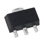
| 描述 | IC AMP GAIN BLOCK 17DB SOT89-3射频放大器 30MHz-6GHz RF/IF Gain Block |
| 产品分类 | |
| 品牌 | Analog Devices Inc |
| 产品手册 | |
| 产品图片 |
|
| rohs | 符合RoHS无铅 / 符合限制有害物质指令(RoHS)规范要求 |
| 产品系列 | RF集成电路,射频放大器,Analog Devices ADL5544ARKZ-R7- |
| 数据手册 | |
| P1dB | 17.6dBm (57.5mW) |
| 产品型号 | ADL5544ARKZ-R7 |
| RF类型 | 通用 |
| 产品种类 | 射频放大器 |
| 供应商器件封装 | SOT-89-3 |
| 其它名称 | ADL5544ARKZ-R7DKR |
| 功率增益类型 | 17.4 dB |
| 包装 | Digi-Reel® |
| 商标 | Analog Devices |
| 噪声系数 | 2.9dB |
| 增益 | 17.4dB |
| 安装风格 | SMD/SMT |
| 封装 | Reel |
| 封装/外壳 | TO-243AA |
| 封装/箱体 | SOT-89-3 |
| 工作电源电压 | 5 V |
| 工作频率 | 30 MHz to 6 GHz |
| 工厂包装数量 | 1000 |
| 最大功率耗散 | 275 mW |
| 最大工作温度 | + 105 C |
| 最小工作温度 | - 40 C |
| 标准包装 | 1 |
| 测试频率 | 900MHz |
| 特色产品 | http://www.digikey.cn/product-highlights/zh/adl554x-adl561x-rfif-gain-blocks/51006http://www.digikey.cn/product-highlights/cn/zh/analog-devices-select-products/4035 |
| 电压-电源 | 4.75 V ~ 5.25 V |
| 电流-电源 | 55mA |
| 电源电流 | 55 mA |
| 类型 | Gain Block Amplifier |
| 输出截获点 | 34.9 dBm |
| 配用 | /product-detail/zh/ADL5544-EVALZ/ADL5544-EVALZ-ND/4866716 |
| 频率 | 30MHz ~ 6GHz |


- 商务部:美国ITC正式对集成电路等产品启动337调查
- 曝三星4nm工艺存在良率问题 高通将骁龙8 Gen1或转产台积电
- 太阳诱电将投资9.5亿元在常州建新厂生产MLCC 预计2023年完工
- 英特尔发布欧洲新工厂建设计划 深化IDM 2.0 战略
- 台积电先进制程称霸业界 有大客户加持明年业绩稳了
- 达到5530亿美元!SIA预计今年全球半导体销售额将创下新高
- 英特尔拟将自动驾驶子公司Mobileye上市 估值或超500亿美元
- 三星加码芯片和SET,合并消费电子和移动部门,撤换高东真等 CEO
- 三星电子宣布重大人事变动 还合并消费电子和移动部门
- 海关总署:前11个月进口集成电路产品价值2.52万亿元 增长14.8%


PDF Datasheet 数据手册内容提取
30 MHz to 6 GHz RF/IF Gain Block Data Sheet ADL5544 FEATURES FUNCTIONAL BLOCK DIAGRAM Fixed gain of 17.4 dB GND Broadband operation from 30 MHz to 6 GHz (2) Input/output internally matched to 50 Ω ADL5544 Integrated bias control circuit OIP3 of 34.9 dBm at 900 MHz BIAS PN1odisBe ofifg 1u7r.e6 o dfB 2m.9 a dtB 9 a0t0 9 M0H0 zM Hz RF1IN GN2D RFO3UT 11384-001 Single 5 V power supply Figure 1. Low quiescent current of 55 mA Wide operating temperature range of −40°C to +105°C Thermally efficient SOT-89 package ESD rating of ±1.5 kV (Class 1C) GENERAL DESCRIPTION The ADL5544 is a single-ended RF/IF gain block amplifier The ADL5544 is fabricated on an InGaP HBT process and has that provides broadband operation from 30 MHz to 6 GHz. a high ESD rating of ±1.5 kV (Class 1C). The ADL5544 is also The ADL5544 provides over 34 dBm of OIP3 using only 55 mA fully specified for operation across the wide temperature range of from a 5 V supply. −40°C to +105°C. A fully populated RoHS-compliant evaluation board is available. The ADL5544 provides a gain of 17 dB, which is stable over frequency, temperature, power supply, and from device to device. The amplifier is offered in the industry-standard SOT-89 package and is internally matched to 50 Ω at the input and output, making the ADL5544 very easy to implement in a wide variety of applica- tions. The only external components required are the input/output ac coupling capacitors, power supply decoupling capacitors, and dc bias inductor. Rev. A Document Feedback Information furnished by Analog Devices is believed to be accurate and reliable. However, no responsibility is assumed by Analog Devices for its use, nor for any infringements of patents or other One Technology Way, P.O. Box 9106, Norwood, MA 02062-9106, U.S.A. rights of third parties that may result from its use. Specifications subject to change without notice. No license is granted by implication or otherwise under any patent or patent rights of Analog Devices. Tel: 781.329.4700 ©2013 Analog Devices, Inc. All rights reserved. Trademarks and registered trademarks are the property of their respective owners. Technical Support www.analog.com
ADL5544 Data Sheet TABLE OF CONTENTS Features .............................................................................................. 1 100 MHz to 500 MHz Frequency Band .................................. 10 Functional Block Diagram .............................................................. 1 4 GHz to 6 GHz Frequency Band ............................................ 11 General Description ......................................................................... 1 General......................................................................................... 12 Revision History ............................................................................... 2 Applications Information .............................................................. 14 Specifications ..................................................................................... 3 Basic Connections ...................................................................... 14 Typical Scattering Parameters (S-Parameters) ......................... 5 Soldering Information and Recommended Absolute Maximum Ratings ............................................................ 7 PCB Land Pattern ....................................................................... 15 Thermal Resistance ...................................................................... 7 Operation Down to 30 MHz ..................................................... 16 ESD Caution .................................................................................. 7 W-CDMA ACPR Performance ................................................ 16 Pin Configuration and Function Descriptions ............................. 8 Evaluation Board ............................................................................ 17 Typical Performance Characteristics ............................................. 9 Outline Dimensions ....................................................................... 18 500 MHz to 4 GHz Frequency Band .......................................... 9 Ordering Guide .......................................................................... 18 REVISION HISTORY 11/13—Rev. 0 to Rev. A Added Figure 25, Renumbered Sequentially .............................. 12 Changes to Figure 34 ...................................................................... 15 Updated Outline Dimensions ....................................................... 18 4/13—Revision 0: Initial Version Rev. A | Page 2 of 20
Data Sheet ADL5544 SPECIFICATIONS V = 5 V and T = 25°C, unless otherwise noted. POS A Table 1. Parameter Test Conditions/Comments Min Typ Max Unit OVERALL FUNCTION Frequency Range 30 6000 MHz FREQUENCY = 30 MHz Gain 18.5 dB Output 1 dB Compression Point 13.0 dBm Output Third-Order Intercept Δf = 1 MHz, output power (P ) = −7 dBm per tone 31.2 dBm OUT Noise Figure 3.9 dB FREQUENCY = 140 MHz Gain 18.04 dB vs. Frequency ±10 MHz ±0.04 dB vs. Temperature −40°C ≤ T ≤ +85°C ±0.3 dB A vs. Supply 4.75 V to 5.25 V ±0.05 dB Output 1 dB Compression Point 16.9 dBm Output Third-Order Intercept Δf = 1 MHz, output power (P ) = −7 dBm per tone 32.0 dBm OUT Noise Figure 3.1 dB FREQUENCY = 350 MHz Gain 17.8 dB vs. Frequency ±10 MHz ±0.01 dB vs. Temperature −40°C ≤ T ≤ +85°C ±0.3 dB A vs. Supply 4.75 V to 5.25 V ±0.06 dB Output 1 dB Compression Point 17.4 dBm Output Third-Order Intercept Δf = 1 MHz, output power (P ) = −7 dBm per tone 31.2 dBm OUT Noise Figure 3.1 dB FREQUENCY = 700 MHz Gain 17.1 17.6 18.0 dB vs. Frequency ±50 MHz ±0.03 dB vs. Temperature −40°C ≤ T ≤ +85°C ±0.3 dB A vs. Supply 4.75 V to 5.25 V ±0.02 dB Output 1 dB Compression Point 17.4 dBm Output Third-Order Intercept Δf = 1 MHz, output power (P ) = −7 dBm per tone 33.4 dBm OUT Noise Figure 2.9 dB FREQUENCY = 900 MHz Gain 17.0 17.4 17.8 dB vs. Frequency ±50 MHz ±0.03 dB vs. Temperature −40°C ≤ T ≤ +85°C ±0.3 dB A vs. Supply 4.75 V to 5.25 V ±0.02 dB Output 1 dB Compression Point 17.6 dBm Output Third-Order Intercept Δf = 1 MHz, output power (P ) = −7 dBm per tone 34.9 dBm OUT Noise Figure 2.9 dB FREQUENCY = 1900 MHz Gain 16.2 16.6 17.0 dB vs. Frequency ±50 MHz ±0.05 dB vs. Temperature −40°C ≤ T ≤ +85°C ±0.3 dB A vs. Supply 4.75 V to 5.25 V ±0.04 dB Output 1 dB Compression Point 15.4 dBm Output Third-Order Intercept Δf = 1 MHz, output power (P ) = −7 dBm per tone 32.4 dBm OUT Noise Figure 3.4 dB Rev. A | Page 3 of 20
ADL5544 Data Sheet Parameter Test Conditions/Comments Min Typ Max Unit FREQUENCY = 2140 MHz Gain 15.9 16.4 16.7 dB vs. Frequency ±50 MHz ±0.04 dB vs. Temperature −40°C ≤ T ≤ +85°C ±0.4 dB A vs. Supply 4.75 V to 5.25 V ±0.05 dB Output 1 dB Compression Point 14.8 dBm Output Third-Order Intercept Δf = 1 MHz, output power (P ) = −7 dBm per tone 31.3 dBm OUT Noise Figure 3.5 dB FREQUENCY = 2600 MHz Gain 15.6 16.0 16.4 dB vs. Frequency ±50 MHz ±0.03 dB vs. Temperature −40°C ≤ T ≤ +85°C ±0.3 dB A vs. Supply 4.75 V to 5.25 V ±0.05 dB Output 1 dB Compression Point 14.1 dBm Output Third-Order Intercept Δf = 1 MHz, output power (P ) = −7 dBm per tone 30.0 dBm OUT Noise Figure 3.7 dB FREQUENCY = 3500 MHz Gain 15.2 15.6 16.1 dB vs. Frequency ±50 MHz ±0.05 dB vs. Temperature −40°C ≤ T ≤ +85°C ±0.4 dB A vs. Supply 4.75 V to 5.25 V ±0.03 dB Output 1 dB Compression Point 12.2 dBm Output Third-Order Intercept Δf = 1 MHz, output power (P ) = −7 dBm per tone 26.0 dBm OUT Noise Figure 4.1 dB FREQUENCY = 4000 MHz Gain 14.4 15.0 15.5 dB vs. Frequency ±50 MHz ±0.10 dB vs. Temperature −40°C ≤ T ≤ +85°C ±0.6 dB A vs. Supply 4.75 V to 5.25 V ±0.08 dB Output 1 dB Compression Point 10.8 dBm Output Third-Order Intercept Δf = 1 MHz, output power (P ) = −7 dBm per tone 23.8 dBm OUT Noise Figure 4.6 dB FREQUENCY = 5000 MHz Gain 14.0 dB vs. Frequency ±50 MHz ±0.04 dB vs. Temperature −40°C ≤ T ≤ +85°C ±0.6 dB A vs. Supply 4.75 V to 5.25 V ±0.10 dB Output 1 dB Compression Point 8.7 dBm Output Third-Order Intercept Δf = 1 MHz, output power (P ) = −7 dBm per tone 21.3 dBm OUT Noise Figure 4.8 dB FREQUENCY = 5800 MHz Gain 14.5 dB vs. Frequency ±50 MHz ±0.15 dB vs. Temperature −40°C ≤ T ≤ +85°C ±1.0 dB A vs. Supply 4.75 V to 5.25 V ±0.10 dB Output 1 dB Compression Point 7.0 dBm Output Third-Order Intercept Δf = 1 MHz, output power (P ) = −7 dBm per tone 18.7 dBm OUT Noise Figure 5.4 dB POWER INTERFACE V POS Supply Voltage 4.75 5 5.25 V Supply Current 55 69 mA vs. Temperature −40°C ≤ T ≤ +85°C −5 mA A Power Dissipation V = 5 V 275 mW POS Rev. A | Page 4 of 20
Data Sheet ADL5544 TYPICAL SCATTERING PARAMETERS (S-PARAMETERS) V = 5 V and T = 25°C. The effects of the test fixture have been deembedded up to the pins of the device. POS A Table 2. Frequency S11 S21 S12 S22 (MHz) Magnitude (dB) Angle (°) Magnitude (dB) Angle (°) Magnitude (dB) Angle (°) Magnitude (dB) Angle (°) 30 −9.75838 −92.0495 19.91469 160.691 −21.4134 19.08688 −10.175 −100.818 50 −13.0161 −114.478 18.9406 163.9441 −21.1763 10.75632 −12.7436 −124.228 100 −15.8296 −142.951 18.34431 167.4073 −21.0719 3.454046 −14.8272 −150.688 200 −16.7468 −164.185 18.13374 166.5362 −21.059 −2.10036 −15.7366 −169.056 300 −16.7917 −173.294 18.0488 163.4408 −21.0741 −5.56114 −15.9476 −177.5 400 −16.7639 −178.57 17.97824 159.7115 −21.0901 −8.54887 −15.9985 177.0591 500 −16.6368 176.8142 17.91669 155.6494 −21.1284 −11.3218 −15.9997 172.8508 600 −16.5495 172.727 17.85356 151.5874 −21.1641 −13.9309 −15.9194 169.301 700 −16.4931 169.7664 17.77106 147.4093 −21.2044 −16.5131 −15.8227 166.4768 800 −16.4227 166.4253 17.71131 143.3218 −21.2438 −19.0298 −15.7257 163.7476 900 −16.3553 163.4457 17.66826 139.1424 −21.2871 −21.5022 −15.5947 162.0291 1000 −16.4799 160.784 17.58888 134.9062 −21.3302 −23.9656 −15.6619 160.4644 1100 −16.4953 158.6829 17.53756 130.7521 −21.3803 −26.4082 −15.644 159.4497 1200 −16.7606 157.8074 17.47488 126.5829 −21.4161 −28.8192 −15.8311 159.6244 1300 −16.9103 157.3382 17.44318 122.3575 −21.4674 −31.2788 −15.9907 159.7403 1400 −17.2225 158.2929 17.38821 118.1946 −21.5203 −33.7399 −16.21 160.9107 1500 −17.6402 160.1629 17.33858 114.0765 −21.5672 −36.1081 −16.539 162.8989 1600 −18.0653 164.333 17.32871 109.7247 −21.6024 −38.6986 −16.7579 165.3782 1700 −18.5601 169.5526 17.27848 105.5495 −21.6825 −41.0309 −17.0431 169.2425 1800 −19.01 177.6071 17.22524 101.4425 −21.7323 −43.4108 −17.1957 174.945 1900 −19.1982 −173.627 17.19407 97.28532 −21.7873 −45.7867 −17.2297 −179.104 2000 −19.156 −163.672 17.14779 93.09047 −21.8417 −48.1855 −17.0968 −171.974 2100 −18.7447 −154.484 17.1201 88.86399 −21.8994 −50.5584 −16.8241 −164.872 2200 −18.2725 −146.868 17.06239 84.78041 −21.9604 −52.8879 −16.481 −158.228 2300 −17.5769 −140.357 17.00071 80.71247 −22.0229 −55.1919 −16.0694 −152.253 2400 −16.9363 −136.067 16.97464 76.65373 −22.0831 −57.4478 −15.6966 −147.411 2500 −16.3707 −133.128 16.91632 72.6253 −22.1477 −59.6933 −15.4361 −143.919 2600 −15.8425 −131.025 16.84092 68.6308 −22.2125 −61.938 −15.2228 −141.803 2700 −15.4474 −130.097 16.80102 64.69363 −22.2782 −64.111 −15.209 −141.248 2800 −15.1642 −129.731 16.74106 60.74876 −22.3485 −66.3047 −15.2585 −142.511 2900 −14.9231 −130.057 16.68572 56.76032 −22.4164 −68.5093 −15.3514 −145.642 3000 −14.8791 −130.912 16.64527 52.71256 −22.4858 −70.6726 −15.4628 −150.396 3100 −14.8847 −132.738 16.56622 48.69909 −22.5616 −72.9343 −15.4514 −156.986 3200 −14.9364 −134.966 16.51404 44.62054 −22.636 −75.1868 −15.2627 −164.185 3300 −15.1065 −138.423 16.45702 40.56141 −22.7184 −77.4701 −14.9704 −171.492 3400 −15.2148 −142.265 16.38871 36.48298 −22.8123 −79.8304 −14.4379 −178.173 3500 −15.2414 −147.094 16.3331 32.32549 −22.9021 −82.0942 −13.8431 175.3551 3600 −15.0937 −152.434 16.26873 28.0511 −23.0024 −84.4293 −13.2863 169.8835 3700 −14.8339 −157.56 16.2039 23.84273 −23.1015 −86.7756 −12.7034 164.8455 3800 −14.3558 −162.074 16.11548 19.63339 −23.2085 −89.1254 −12.1263 160.5459 3900 −13.7757 −166.117 16.03442 15.32869 −23.3318 −91.426 −11.5679 156.6935 4000 −13.0504 −169.18 15.92646 11.18556 −23.4494 −93.8454 −10.9616 153.5414 4100 −12.3247 −171.219 15.82941 6.975896 −23.577 −96.1196 −10.3638 151.0243 4200 −11.6347 −173.249 15.72571 2.726895 −23.7138 −98.3778 −9.78722 149.3781 4300 −10.9654 −174.775 15.58441 −1.36477 −23.8541 −100.612 −9.23037 148.452 4440 −10.2422 −176.69 15.44684 −7.08335 −24.0446 −103.673 −8.61459 148.1682 4500 −9.95152 −177.613 15.38641 −9.50947 −24.1234 −104.95 −8.40319 148.3894 4600 −9.51739 −178.831 15.2557 −13.503 −24.2418 −107.053 −8.1407 148.9119 Rev. A | Page 5 of 20
ADL5544 Data Sheet Frequency S11 S21 S12 S22 (MHz) Magnitude (dB) Angle (°) Magnitude (dB) Angle (°) Magnitude (dB) Angle (°) Magnitude (dB) Angle (°) 4700 −9.15961 179.4184 15.18857 −17.5037 −24.3599 −109.077 −8.00124 149.4702 4800 −8.81402 177.4327 15.08704 −21.4903 −24.4618 −111.079 −7.96813 149.7089 4900 −8.53104 175.2276 14.98061 −25.462 −24.5534 −113.068 −8.06461 149.4032 5000 −8.30896 172.6355 14.92996 −29.3613 −24.6449 −114.946 −8.27561 148.5568 5100 −8.09121 170.0194 14.84603 −33.2282 −24.7131 −116.819 −8.51734 146.6025 5200 −7.92674 167.1306 14.7721 −37.1236 −24.7652 −118.67 −8.77718 143.5944 5300 −7.79364 163.9153 14.72301 −41.0236 −24.8151 −120.546 −8.99346 139.518 5400 −7.6793 160.6589 14.64549 −45.0881 −24.8399 −122.534 −9.12197 134.7305 5500 −7.61523 156.9392 14.59131 −49.1815 −24.8628 −124.569 −9.17338 129.7103 5600 −7.60815 152.7976 14.53579 −53.2876 −24.8758 −126.604 −9.15423 124.593 5700 −7.54914 148.5617 14.47484 −57.5187 −24.8597 −128.793 −9.05211 119.5068 5800 −7.51209 143.7768 14.45495 −61.7253 −24.8296 −131.021 −9.00726 114.4158 5900 −7.46152 138.6641 14.42222 −66.0417 −24.7902 −133.375 −9.00598 109.1347 6000 −7.35914 133.6743 14.38015 −70.439 −24.7398 −135.849 −9.00546 103.4141 Rev. A | Page 6 of 20
Data Sheet ADL5544 ABSOLUTE MAXIMUM RATINGS THERMAL RESISTANCE Table 3. Parameter Rating Table 4 lists the junction-to-air thermal resistance (θ ) and the JA Supply Voltage, VPOS 6.5 V junction-to-case thermal resistance (θJC) for the ADL5544. Input Power (50 Ω Impedance) 18 dBm Table 4. Thermal Resistance Internal Power Dissipation 400 mW (Pad Soldered to Ground) Package Type θJA1 θJC2 Unit Maximum Junction Temperature 150°C 3-Lead SOT-89 (RK-3) 53 15 °C/W Operating Temperature Range −40°C to +105°C 1 Measured on the ADL5544 evaluation board. For more information about Storage Temperature Range −65°C to +150°C board layout, see the Soldering Information and Recommended PCB Land Pattern section. 2 Based on simulation with a standard JEDEC board per JESD51. Stresses above those listed under Absolute Maximum Ratings may cause permanent damage to the device. This is a stress ESD CAUTION rating only; functional operation of the device at these or any other conditions above those indicated in the operational section of this specification is not implied. Exposure to absolute maximum rating conditions for extended periods may affect device reliability. Rev. A | Page 7 of 20
ADL5544 Data Sheet PIN CONFIGURATION AND FUNCTION DESCRIPTIONS RFIN 1 ADL5544 GND 2 TOP VIEW (2) GND (Not to Scale) RFOUT 3 NOTES 1.THE EXPOSED PAD ENCOMPASSES PIN 2 AND THE TTPTAHHLABEE NR EAEMXT AP FTLOOH RSTEER ETDALO NEPPSCA FSTDEIR DTRIECO. A OALF L GTORHWOE UIPMNAPDCEIKNDAGAG NAECN.E DS GORLDOEURND 11384-002 Figure 2. Pin Configuration Table 5. Pin Function Descriptions Pin No. Mnemonic Description 1 RFIN RF Input. This pin requires a dc blocking capacitor. 2 GND Ground. Connect this pin to a low impedance ground plane. 3 RFOUT RF Output and Supply Voltage. DC bias is provided to this pin through an inductor that is connected to the external power supply. The RF path requires a dc blocking capacitor. EPAD Exposed Pad. The exposed pad encompasses Pin 2 and the tab at the top side of the package. Solder the exposed pad to a low impedance ground plane for electrical grounding and thermal transfer. Rev. A | Page 8 of 20
Data Sheet ADL5544 TYPICAL PERFORMANCE CHARACTERISTICS 500 MHz TO 4 GHz FREQUENCY BAND 40 40 m) B, dB 35 35 900MHz d OIP3 ( 30 OIP3 700MHz 2140MHz 1900MHz dB, 25 m) 30 1 B GAIN, P 20 GAIN OIP3 (d 25 3500MHz 2600MHz E, 15 UR P1dB 4000MHz G 10 E FI 20 OIS 5 NOISE FIGURE N 00.5 1.0 1.5 FRE2Q.0UENCY2 (.G5Hz) 3.0 3.5 4.0 11384-003 15–12 –10 POUT– 8PER TONE –(d6Bm) –4 –2 11384-006 Figure 3. Noise Figure, Gain, P1dB, and OIP3 vs. Frequency Figure 6. OIP3 vs. Output Power (POUT) and Frequency 19.0 0 18.5 –5 18.0 –40°C B) 1177..50 +25°C RS (dB) –10 d E S22 N ( 16.5 ET –15 GAI 16.0 RAM A 15.5 +85°C S-P –20 S12 S11 +105°C 15.0 –25 14.5 14.00.5 1.0 1.5 FRE2Q.0UENCY2 (.G5Hz) 3.0 3.5 4.0 11384-004 –300.5 1.0 1.5 FRE2Q.0UENCY2 (.G5Hz) 3.0 3.5 4.0 11384-007 Figure 4. Gain vs. Frequency and Temperature Figure 7. Input Return Loss (S11), Output Return Loss (S22), and Reverse Isolation (S12) vs. Frequency 40 40 6.0 –40°C 35 +25°C 35 5.5 +85°C 5.0 30 30 B) +105°C P1dB (dBm) 2250 +85°C +105°C +25°C –40°C 2250 OIP3 (dBm) NOISE FIGURE (d 344...505 +25°C 15 15 –40°C 3.0 10 10 2.5 +105°C +85°C 50.5 1.0 1.5 FRE2Q.0UENCY2 (.G5Hz) 3.0 3.5 4.05 11384-005 2.00.5 1.0 1.5 FRE2Q.0UENCY2 (.G5Hz) 3.0 3.5 4.0 11384-008 Figure 5. P1dB and OIP3 vs. Frequency and Temperature Figure 8. Noise Figure vs. Frequency and Temperature Rev. A | Page 9 of 20
ADL5544 Data Sheet 100 MHz TO 500 MHz FREQUENCY BAND 35 35 m) OIP3 B d 30 B, 33 d P3 ( 25 140MHz OI P1dB, 20 GAIN dBm) 31 350MHz GAIN, 15 P1dB OIP3 ( 29 E, R U 10 G E FI 27 S 5 OI NOISE FIGURE N 00.10 0.15 0.20 0F.R25EQUE0N.3C0Y (G0H.3z5) 0.40 0.45 0.50 11384-009 25–12 –10 POUT– 8PER TONE– (6dBm) –4 –2 11384-012 Figure 9. Noise Figure, Gain, P1dB, and OIP3 vs. Frequency, Figure 12. OIP3 vs. Output Power (POUT) and Frequency, Low Frequency Configuration Low Frequency Configuration 19.0 0 18.5 –40°C +25°C –5 18.0 dB) –10 B) 17.5 RS ( N (d 17.0 +85°C ETE –15 S22 GAI +105°C RAM S11 16.5 A S-P –20 16.0 S12 –25 15.5 15.00.10 0.15 0.20 0F.R25EQUE0N.3C0Y (G0H.3z5) 0.40 0.45 0.50 11384-010 –300.10 0.15 0.20 0F.R25EQUE0N.3C0Y (G0H.3z5) 0.40 0.45 0.50 11384-013 Figure 10. Gain vs. Frequency and Temperature, Figure 13. Input Return Loss (S11), Output Return Loss (S22), and Reverse Low Frequency Configuration Isolation (S12) vs. Frequency, Low Frequency Configuration 40 40 6.0 +25°C 35 –40°C 35 5.5 5.0 30 30 B) P1dB (dBm) 2250 +25°C +85°C +105°C +85°C 2250 OIP3 (dBm) OISE FIGURE (d 344...505 +105°C +85°C N +25°C 15 15 3.0 –40°C +105°C –40°C 10 10 2.5 50.10 0.15 0.20 0F.R25EQUE0N.3C0Y (G0H.3z5) 0.40 0.45 0.505 11384-011 2.00.10 0.15 0.20 0F.R25EQUE0N.3C0Y (G0H.3z5) 0.40 0.45 0.50 11384-014 Figure 11. P1dB and OIP3 vs. Frequency and Temperature, Figure 14. Noise Figure vs. Frequency and Temperature, Low Frequency Configuration Low Frequency Configuration Rev. A | Page 10 of 20
Data Sheet ADL5544 4 GHz TO 6 GHz FREQUENCY BAND 25 25 m) B OIP3 d B, 20 23 d 3 ( P OI 5000MHz dB, 15 m) 21 1 B P GAIN d N, 3 ( GAI 10 OIP 19 E, R P1dB 5800MHz U G E FI 5 17 OIS NOISE FIGURE N 04.0 4.2 4.4 4.6 FR4E.8QUE5N.0CY (G5.H2z) 5.4 5.6 5.8 6.0 11384-015 15–12 –10 POUT– 8PER TONE– (6dBm) –4 –2 11384-018 Figure 15. Noise Figure, Gain, P1dB, and OIP3 vs. Frequency, Figure 18. OIP3 vs. Output Power (POUT) and Frequency, High Frequency Configuration High Frequency Configuration 16.0 0 15.5 –40°C –5 15.0 +25°C 14.5 dB) –10 S11 B) 14.0 RS ( S22 d E N ( 13.5 ET –15 GAI 13.0 RAM A 12.5 +85°C +105°C S-P –20 12.0 S12 –25 11.5 11.04.0 4.2 4.4 4.6 FR4E.8QUE5N.0CY (G5.H2z) 5.4 5.6 5.8 6.0 11384-016 –304.0 4.2 4.4 4.6 FR4E.8QUE5N.0CY (G5.H2z) 5.4 5.6 5.8 6.0 11384-019 Figure 16. Gain vs. Frequency and Temperature, Figure 19. Input Return Loss (S11), Output Return Loss (S22), and Reverse High Frequency Configuration Isolation (S12) vs. Frequency, High Frequency Configuration 40 40 8.0 7.5 35 35 7.0 30 30 P1dB (dBm) 221505 +25°C –+4205°°CC +85°C +105°C 221505 OIP3 (dBm) OISE FIGURE (dB) 5566....0505 +105°C ++2855°°CC –40°C N 4.5 10 10 –40°C 4.0 5 5 3.5 +85°C +105°C 04.0 4.2 4.4 4.6 FR4E.8QUE5N.0CY (G5.H2z) 5.4 5.6 5.8 6.00 11384-017 3.04.0 4.2 4.4 4.6 FR4E.8QUE5N.0CY (G5.H2z) 5.4 5.6 5.8 6.0 11384-020 Figure 17. P1dB and OIP3 vs. Frequency and Temperature, Figure 20. Noise Figure vs. Frequency and Temperature, High Frequency Configuration High Frequency Configuration Rev. A | Page 11 of 20
ADL5544 Data Sheet GENERAL 65 70 63 68 61 66 mA) 59 mA) 64 T ( 5.25V T ( N 57 N 62 E 5.00V E R R UR 55 UR 60 LY C 53 4.75V LY C 58 5.25V P P P P U 51 U 56 5.00V S S 49 54 4.75V 47 52 45–40–30–20–10 0 10TE2M0PE3R0AT4U0RE5 0(°C6)0 70 80 90 100110 11384-021 501 3 5 7 PO9UT (dB1m1) 13 15 17 19 11384-024 Figure 21. Supply Current vs. Temperature Figure 24. Supply Current vs. POUT at 900 MHz 60 61 59 50 A) 57 E (%) 40 NT (m 55 +25°C G E NTA 30 URR 53 +85°C E C C Y ER PL 51 +105°C P 20 P U S 49 –40°C 10 47 0 17.0 17.1 17.2 17G.A3IN (d1B7.)4 17.5 17.6 17.7 11384-022 45–16–14–12–10–8 –6 –4 –2PO0UT 2(dB4m)6 8 10 12 14 16 18 20 11384-100 Figure 22. Gain Distribution at 900 MHz Figure 25. Supply Current vs. POUT and Temperature at 900 MHz 18 45 16 40 14 35 %) 12 %) 30 E ( E ( AG 10 AG 25 NT NT E 8 E 20 C C R R PE 6 PE 15 4 10 2 5 0 16.9 17.0 17.1 17.2 17.3P117d.B4 (1d7B.5m)17.6 17.7 17.8 17.9 18.0 11384-023 0 31 32 33 O34IP3 (dB3m5) 36 37 38 11384-025 Figure 23. P1dB Distribution at 900 MHz Figure 26. OIP3 Distribution at 900 MHz, POUT = −7 dBm per Tone Rev. A | Page 12 of 20
Data Sheet ADL5544 70 0 –10 60 –20 50 %) Bc) –30 GE ( 40 S (d –40 A C CENT 30 MONI –50 H2 R R PE HA –60 20 H3 –70 10 –80 0 2.6 2.7 2N.8OISE F2IG.9URE (d3B.0) 3.1 3.2 11384-026 –900.5 1.0 1.5 FRE2Q.0UENCY2 .(5GHz) 3.0 3.5 4.0 11384-027 Figure 27. Noise Figure Distribution at 900 MHz Figure 28. Single-Tone Harmonics vs. Frequency, POUT = 0 dBm Rev. A | Page 13 of 20
ADL5544 Data Sheet APPLICATIONS INFORMATION BASIC CONNECTIONS 35 m) Figure 29 shows the basic connections for operating the dB 30 ADL5544. The device supports operation from 30 MHz to 6 GHz. dB, However, for optimal performance at lower and higher frequency P3 ( 25 OOIIPP33,, DLOEFWA UFRLTE QSUEETUNPC YC OCONFNIFGIGURUARTAITOIONN OI GAIN, DEFAULT SETUP CONFIGURATION bands, the board configuration must be adjusted. Table 6 lists B, GAIN, LOW FREQUENCY CONFIGURATION d 20 the recommended board configuration to operate the device at P1 N, various frequency bands. AI 15 G GND VPOS RE, P1dB, DEFAULT SETUP CONFIGURATION C6 FIGU 10 NP1OdISBE, LFOIGWU FRREE, QDEUFEANUCLYT C SOENTFUIPG UCROANTFIIOGNURATION (2) GND 1C0µ5F NOISE 5 NOISE FIGURE, LOW FREQUENCY CONFIGURATION ADL5544 1Cn4F 00.10 0.15 0.20 0F.R25EQUE0N.3C0Y (G0H.3z5) 0.40 0.45 0.50 11384-029 100pF Figure 30. Noise Figure, Gain, P1dB, and OIP3 vs. Frequency, RFIN C1 RFIN1 GND2 RFOUT3 L1 C2 RFOUT with1 t0h0e MOpHtzi mtoi z5e0d0 S MetHtizn, gCso amnpda trhiseo Dne ofaf uPeltr Cfoornmfiagnucrea t ion C7 C8 11384-028 0 SS1111,, DLOEFWA UFRLTE QSUEETUNPC YC OCONFNIFGIGURUARTAITOIONN Figure 29. Basic Connections S22, DEFAULT SETUP CONFIGURATION –5 S22, LOW FREQUENCY CONFIGURATION S12, DEFAULT SETUP CONFIGURATION A 5 V dc bias is supplied to the amplifier through the bias S12, LOW FREQUENCY CONFIGURATION inductor connected to RFOUT (Pin 3). The bias voltage must dB) –10 be decoupled using 100 pF, 1 nF, and 10 µF power supply RS ( E decoupling capacitors. The typical current consumption for ET –15 M the ADL5544 is 55 mA. RA A At low and high frequencies, the device exhibits improved S-P –20 performance with the suggested setup configuration listed in –25 Table 6. Figure 30 to Figure 33 provide a comparison of the performance of the device at the 100 MHz to 500 MHz and 4co GnHfigzu troa t6i oGnH azn db atnhde sd wefhaeunlt dsreitvuepn c wonitfhig tuhrea otipotnim. al setup –300.10 0.15 0.20 0F.R25EQUE0N.3C0Y (G0H.3z5) 0.40 0.45 0.50 11384-030 Figure 31. Return Loss and Reverse Isolation, 100 MHz to 500 MHz, Comparison of Performance with the Optimized Settings and the Default Configuration Table 6. Recommended Components for Basic Connections High Frequency Matching AC Coupling Capacitors (0402) DC Bias Inductor (0603HP) Capacitors (0402) Frequency Band C1 C2 L1 C7 C8 100 MHz to 500 MHz 100 nF 100 nF 1000 nH Do not install Do not install 500 MHz to 4 GHz (default) 100 pF 100 pF 100 nH Do not install Do not install 4 GHz to 6 GHz 100 pF 100 pF 12 nH 0.1 pF 0.1 pF Rev. A | Page 14 of 20
Data Sheet ADL5544 25 SOLDERING INFORMATION AND RECOMMENDED m) PCB LAND PATTERN B d OIP3 (dB, 20 GOOAIIPPI33N,,, DHDEIEGFFHAA UFULRLTET QSSEUETETUNUPCP YCC OCONONFNFIIFGGIUGURURARATATIITOOINONN FAiDguLr5e5 3444 .s Thoow msi tnhiem riezceo tmhemrmenadl eimd plaendda npcaett, etrhne feoxrp tohsee d pad B, 15 GAIN, HIGH FREQUENCY CONFIGURATION on the underside of the SOT-89 package is soldered to a ground d P1 plane, along with Pin 2. If multiple ground layers exist, stitch N, AI the layers together using vias. G 10 RE, 1.80mm U G E FI 5 S P1dB, DEFAULT SETUP CONFIGURATION OI P1dB, HIGH FREQUENCY CONFIGURATION N NOISE FIGURE, DEFAULT SETUP CONFIGURATION NOISE FIGURE, HIGH FREQUENCY CONFIGURATION 04.0 4.2 4.4 4.6 FR4E.8QUE5N.0CY (G5.H2z) 5.4 5.6 5.8 6.0 11384-031 Figure 32. Noise Figure, Gain, P1dB, and OIP3 vs. Frequency, 4 GHz to 6 GHz, Comparison of Performance with the Optimized Settings and the Default Configuration 0.762mm 0.635mm 0 5.37mm 3.48mm –5 dB) –10 0.20mm S ( R E ET –15 AM S11, DEFAULT SETUP CONFIGURATION R S11, HIGH FREQUENCY CONFIGURATION S-PA –20 SSS122222,,, DDHEEIGFFHAA UUFLLRTTE QSSEEUTTEUUNPPC YCC OOCNNOFFNIIFGGIUUGRRUAARTTAIITOOINNON 0.86mm 0.62mm S12, HIGH FREQUENCY CONFIGURATION –25 1.27mm –304.0 4.2 4.4 4.6 FR4E.8QUE5N.0CY (G5.H2z) 5.4 5.6 5.8 6.0 11384-032 Figure 33. Return Loss and Reverse Isolation, 4 GHz to 6 GHz, Comparison of Performance with the Optimized Settings 0.86mm and the Default Configuration 1.50mm 3.00mm 11384-101 Figure 34. Recommended Land Pattern The land pattern on the ADL5544 evaluation board provides a measured thermal resistance (θ ) of 53°C/W. To measure θ , JA JA the temperature at the top of the SOT-89 package is found with an IR temperature gun. Thermal simulation suggests a junction temperature 10°C higher than the top-of-package temperature. With additional measurements of the ambient temperature and I/O power, θ can be determined. JA Rev. A | Page 15 of 20
ADL5544 Data Sheet OPERATION DOWN TO 30 MHz 32 +25°C To operate the ADL5544 at frequencies below 100 MHz, a feed- 31 –40°C back network must be implemented between the input and output ports of the device to ensure stability. Figure 35 shows a sample 30 configuration used to evaluate the device at frequencies below +85°C m) 1o0f 0th Me dHezv.i Fceig iunr teh 3is6 ctoon Ffiigguurrea t3io8n d.e monstrate the performance P3 (dB 29 +105°C OI GND VPOS 28 C6 ND 10µF 27 (2) G C5 ADL5544 1Cn4F 26–9 –7 POUT PER –T5ONE (dBm) –3 –1 11384-037 RFIN RFIN1 GND2 RFOUT3 L11010000pnFH RFOUT W-CDMA ACPRFi gPuEreR 3F8.O OIRP3M vsA. PNOUCT aEt 3 0 MHz C1 C2 Figure 39 shows a plot of the adjacent channel power ratio 100nF 15R0F0Ω 10CnFF 100nF 11384-034 (sAinCglPeR w) ivdse.b PaOnUdT cfoord teh dei AviDsioLn5 5m44u.l tTiphlee saicgcneasls t(yWpe- CuDseMd iAs )a Figure 35. Setup for Low Frequency Operation Down to 30 MHz carrier (Test Model 1-64) at 2140 MHz. This signal is generated by a very low ACPR source. ACPR is measured at the output by 40 a high dynamic range spectrum analyzer that incorporates an m) B, dB 35 OIP3 instrument noise-correction function. d 0 3 ( 30 P OI c) –10 B, 25 dB P1d ET ( –20 E, GAIN, 1250 PG1AdINB ER OFFS –30 FIGUR 10 CARRI –40 NOISE 5 NOISE FIGURE @ 5MHz ––6500 030 40 50 FRE6Q0UENCY7 (0MHz) 80 90 100 11384-035 ACPR –70 Figure 36. Noise Figure, Gain, P1dB, and OIP3 vs. Frequency, –80 30 MHz to 100 MHz –20 –15 –1P0OUT (dBm–)5 0 5 11384-038 0 Figure 39. ACPR vs. POUT, Single W-CDMA Carrier (Test Model 1-64) at 2140 MHz –5 The ADL5544 achieves an ACPR of −80 dBc at an output power level of −7 dBm, at which point device noise and not distortion S (dB) –10 S11 begins to dominate the power in the adjacent channels. At an ER S22 output power level of 0 dBm, ACPR is still very low at −63 dBc. ET –15 M A R A S-P –20 S12 –25 –3030 40 50 FRE6Q0UENCY7 (0MHz) 80 90 100 11384-036 Figure 37. Return Loss and Reverse Isolation, 30 MHz to 100 MHz Rev. A | Page 16 of 20
Data Sheet ADL5544 EVALUATION BOARD Figure 40 shows the ADL5544 evaluation board layout. GND VSUP Figure 41 shows the schematic for the evaluation board. C6 The board is powered by a single 5 V supply. Table 7 lists ND 10µF the components used on the evaluation board. Power can (2) G C5 be applied to the board through clip-on leads (VSUP, GND). 1nF ADL5544 C4 100pF RFIN RFIN1 GND2 RFOUT3 L1010nH RFOUT 10C01pF 10C02pF 11384-040 Figure 41. Evaluation Board Schematic 11384-039 Figure 40. Evaluation Board Layout (Top) Table 7. Evaluation Board Configuration Options Component Function Default Value C1, C2 AC coupling capacitors 100 pF, 0402 L1 DC bias inductor 100 nH, 0603 (Coilcraft 0603HP or equivalent) V and GND Clip-on terminals for power supply SUP C4, C5, C6 Power supply decoupling capacitors C4: 100 pF, 0603 C5: 1 nF, 0603 C6: 10 μF, 1206 Rev. A | Page 17 of 20
ADL5544 Data Sheet OUTLINE DIMENSIONS 1.75 1.55 2.413 (2) 2.380 2.60 4.25 2.337 2.30 3.94 1 2 3 1.270 0.635 1.252 0.569 1.20 1.219 0.508 BOTTOM VIEW 1.50 TYP 0.75 3.00 TYP TOP VIEW 2.29 4.60 2.14 4.40 1.60 1.40 0.44 0.35 END VIEW 0.56 0.36 0.52 0.32 PKG-003480 COMPLIANT TO JEDEC STANDARDS TO-243 09-12-2013-C Figure 42. 3-Lead Small Outline Transistor Package [SOT-89] (RK-3) Dimensions shown in millimeters ORDERING GUIDE Model1 Temperature Range Package Description Package Option ADL5544ARKZ-R7 −40°C to +105°C 3-Lead SOT-89, 7“ Tape and Reel RK-3 ADL5544-EVALZ −40°C to +105°C Evaluation Board 1 Z = RoHS Compliant Part. Rev. A | Page 18 of 20
Data Sheet ADL5544 NOTES Rev. A | Page 19 of 20
ADL5544 Data Sheet NOTES ©2013 Analog Devices, Inc. All rights reserved. Trademarks and registered trademarks are the property of their respective owners. D11384-0-11/13(A) Rev. A | Page 20 of 20
Mouser Electronics Authorized Distributor Click to View Pricing, Inventory, Delivery & Lifecycle Information: A nalog Devices Inc.: ADL5544ARKZ-R7 ADL5544-EVALZ