ICGOO在线商城 > 射频/IF 和 RFID > RF 放大器 > UPC2746TB-E3-A

 Datasheet下载
- 型号: UPC2746TB-E3-A
- 制造商: CEL
- 库位|库存: xxxx|xxxx
- 要求:
| 数量阶梯 | 香港交货 | 国内含税 |
| +xxxx | $xxxx | ¥xxxx |
查看当月历史价格
查看今年历史价格
UPC2746TB-E3-A产品简介:
ICGOO电子元器件商城为您提供UPC2746TB-E3-A由CEL设计生产,在icgoo商城现货销售,并且可以通过原厂、代理商等渠道进行代购。 UPC2746TB-E3-A价格参考¥5.69-¥5.69。CELUPC2746TB-E3-A封装/规格:RF 放大器, RF Amplifier IC General Purpose 100MHz ~ 1.5GHz 6-SuperMiniMold。您可以下载UPC2746TB-E3-A参考资料、Datasheet数据手册功能说明书,资料中有UPC2746TB-E3-A 详细功能的应用电路图电压和使用方法及教程。
CEL的UPC2746TB-E3-A是一款RF(射频)放大器,属于高性能、低噪声的射频前端器件,广泛应用于需要稳定信号放大和高灵敏度接收的无线通信系统中。该器件典型工作频率范围覆盖UHF至微波频段,适合用于电视调谐器、有线电视(CATV)设备、卫星接收模块以及数字地面广播(如DVB-T/T2、ISDB-T)等场景。

在实际应用中,UPC2746TB-E3-A常被用作高频头(Tuner)中的前置放大器,用于增强接收到的微弱射频信号,提高信噪比和系统接收灵敏度。其低功耗、高增益和优良的噪声系数特性,使其非常适合对信号质量要求较高的消费类电子产品,如数字电视机顶盒、一体机电视、机卡分离式接收设备等。

此外,该芯片采用小型化封装,便于高密度电路布局,适用于空间受限的便携式或紧凑型设备。整体而言,UPC2746TB-E3-A凭借其稳定性与兼容性,在民用广播接收领域具有广泛的应用价值。
| 参数 | 数值 |
| 产品目录 | |
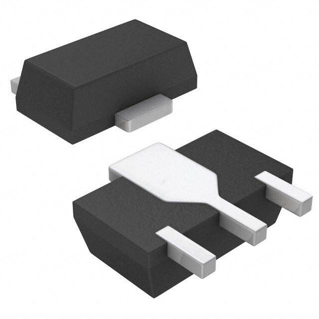
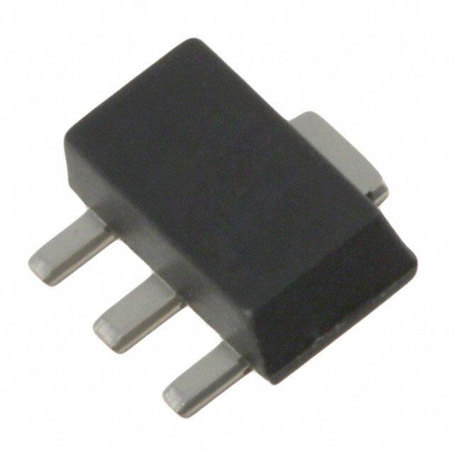
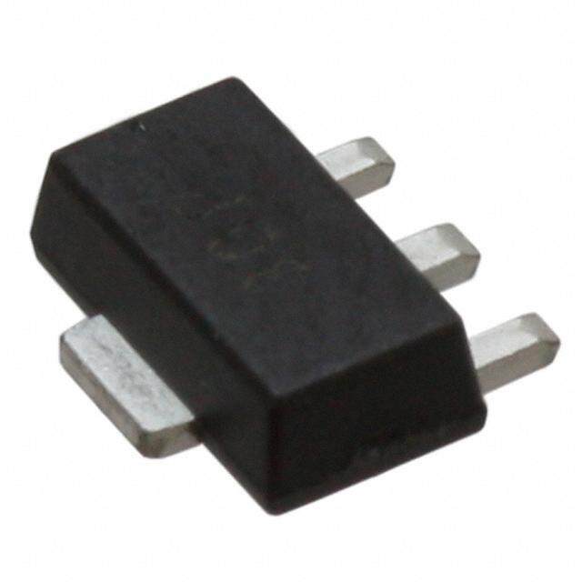
| 描述 | MMIC AMP 1.5GHZ SOT-363射频放大器 3V Widebnd Amplifier |
| 产品分类 | |
| 品牌 | CEL |
| 产品手册 | http://www.cel.com/parts.do?command=load&idRootPart=612# |
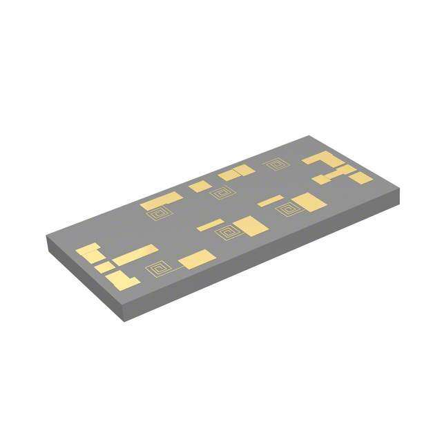
| 产品图片 |
|
| rohs | 符合RoHS无铅 / 符合限制有害物质指令(RoHS)规范要求 |
| 产品系列 | RF集成电路,射频放大器,CEL UPC2746TB-E3-A- |
| 数据手册 | |
| P1dB | - |
| 产品型号 | UPC2746TB-E3-A |
| RF类型 | 通用 |
| 产品目录页面 | |
| 产品种类 | 射频放大器 |
| 供应商器件封装 | 6-SuperMiniMold |
| 其它名称 | UPC2746TB-ACT |
| 功率增益类型 | 19 dB |
| 包装 | 剪切带 (CT) |
| 商标 | CEL |
| 噪声系数 | 4dB |
| 增益 | 19dB |
| 安装风格 | SMD/SMT |
| 封装 | Reel |
| 封装/外壳 | 6-TSSOP,SC-88,SOT-363 |
| 封装/箱体 | Minimold-6 |
| 工作电源电压 | 3 V |
| 工作频率 | 1.5 GHz |
| 工厂包装数量 | 3000 |
| 技术类型 | Variable Gain Amplifiers |
| 最大功率耗散 | 270 mW |
| 最大工作温度 | + 85 C |
| 最小工作温度 | - 40 C |
| 标准包装 | 1 |
| 测试频率 | - |
| 电压-电源 | 1.8 V ~ 3.3 V |
| 电流-电源 | 7.5mA |
| 电源电流 | 7.5 mA |
| 类型 | RF IC |
| 输入返回损失 | 13 dB |
| 隔离分贝 | 45 dB |
| 频率 | 100MHz ~ 1.5GHz |
| 频率范围 | 800 MHz to 900 MHz |


- 商务部:美国ITC正式对集成电路等产品启动337调查
- 曝三星4nm工艺存在良率问题 高通将骁龙8 Gen1或转产台积电
- 太阳诱电将投资9.5亿元在常州建新厂生产MLCC 预计2023年完工
- 英特尔发布欧洲新工厂建设计划 深化IDM 2.0 战略
- 台积电先进制程称霸业界 有大客户加持明年业绩稳了
- 达到5530亿美元!SIA预计今年全球半导体销售额将创下新高
- 英特尔拟将自动驾驶子公司Mobileye上市 估值或超500亿美元
- 三星加码芯片和SET,合并消费电子和移动部门,撤换高东真等 CEO
- 三星电子宣布重大人事变动 还合并消费电子和移动部门
- 海关总署:前11个月进口集成电路产品价值2.52万亿元 增长14.8%


PDF Datasheet 数据手册内容提取
BIPOLAR ANALOG INTEGRATED CIRCUIT PC2745TB,PC2746TB 3 V, SUPER MINIMOLD SILICON MMIC T WIDEBAND AMPLIFIER FOR MOBILE COMMUNICATIONS U DESCRIPTION The PC2745TB and PC2746TB are silicon monolithic integrated circuits designed as buffer amplifier for mobile communications. These low current amplifiers operate on 3.0 V (1.8 V MIN.). These ICs are manufactured using our 20 GHz fT NESATIII silicon bipolar process. This process uses silicon nitride passivation film and gold electrodes. These materials can protect chip sOurface from external pollution and prevent corrosion/migration. Thus, these IC have excellent performance, uniformity and reliability. FEATURES • Supply voltage : Recommended VCC = 2.7 to 3.3 V Circuit operation VCC = 1.8 to -3.3 V • Upper limit operating frequency : PC2745TB; fu = 2.7 GHz TYP.@3 dB bandwidth PC2746TB; fu = 1.5 GHEz TYP.@3 dB bandwidth • High isolation : PC2745TB; ISL = 38 dB TYP.@f = 500 MHz PC2746TB; ISL = 45 dB TYP.@f = 500 MHz • Power gain : PC2745TB; GP = 12 dB TYP.@f = 500 MHz PC2746TB; GP = 19 dB TYP.@f = 500 MHz S • Saturated output power : PC2745TB; PO(sat) = 1 dBm TYP.@f = 500 MHz PC2746TB; PO(sat) = 0 dBm TYP.@f = 500 MHz • High-density surface mounting : 6-pin super minimold package (2.0 1.25 0.9 mm) A APPLICATIONS • 1.5 GHz to 2.5 GHz communication system : PC2745TB • 800 MHz to 900 MHz communication system : PC2746TB ORDERING INFORMATION H Part Number Package Marking Supplying Form PC2745TB-E3-A 6-pin super minimold C1Q • Embossed tape 8 mm wide • 1, 2, 3 pins face the perforation side of the tape P PC2746TB-E3-A C1R • Qty 3 kpcs/reel Remark To order evaluation samples, contact your nearby sales office. Part number for sample order: PC2745TB-A, PC2746TB-A Caution: Observe precautions when handling because these devices are sensitive to electrostatic discharge. Document No. PU10443EJ01V0DS (1st edition) The mark shows major revised points. (Previous No. P11511EJ3V0DS00) Date Published November 2003 CP(K)
PC2745TB,PC2746TB PIN CONNECTION Pin No. Pin Name 1 INPUT 2 GTND 3 GND 4 OUTPUT 5 GND U Marking is an example of PC2745TB 6 VCC PRODUCT LINE-UP (TA = +25C, VCC = 3.0 V, ZS = ZL = 50 ) fu PO(sat) GP NF ICC Part No. OPackage Making (GHz) (dBm) (dB) (dB) (mA) PC2745T 2.7 1.0 12 6.0 7.5 6-pin minimold C1Q PC2745TB 6-pin super minimold PC2746T 1.5 0 19 4.0 7.5 6-pin minimold C1R PC2746TB -6-pin super minimold PC2747T 1.8 7.0 12 3.3 5.0 6-pin minimold C1S E PC2747TB 6-pin super minimold PC2748T 0.2 to 1.5 3.5 19 2.8 6.0 6-pin minimold C1T PC2748TB 6-pin super minimold PC2749T 2.9 6.0 16 4.0 6.0 6-pin minimold C1U S PC2749TB 6-pin super minimold Remark Typical performance. Please refer to ELECTRICAL CHARACTERISTICS in detail. A Caution The package size distinguish between minimold and super minimold. SYSTEM APPLICATION EXAMPLE DIGITAL CELLULAR SYSTEM BLOCK DIAGRAM H P Data Sheet PU10443EJ1V0DS 2
PC2745TB,PC2746TB PIN EXPLANATION Applied Pin Pin Pin Name Voltage Voltage Function and Applications Internal Equivalent Circuit No. Note (V) (V) T 1 INPUT 0.87 Signal input pin. A internal matching circuit, configured with resistors, enables 50 connection over a wide band. this 0.82 pin must be coupled to signal source with U capacitor for DC cut. 2 GND 0 Ground pin. This pin should be connected 3 to system ground with minimum 5 inductance. Ground pattern on the board should be formed as wide as possible. All O the ground pins must be connected together with wide ground pattern to decrease impedance difference. 4 OUTPUT 1.95 Signal output pin. A internal matching circuit, configured with resistors,- enables 50 connection over a wide band. This 2.54 pin must be coupled to next stage with E capacitor for DC cut. 6 VCC 2.7 to Power supply pin. This pin should be 3.3 externally equipped with bypass capacity to minimize ground impedance. S Note Pin voltage is measured at V = 3.0 V. Above: PC2745TB, Below: PC2746TB CC A H P 3 Data Sheet PU10443EJ1V0DS
PC2745TB,PC2746TB ABSOLUTE MAXIMUM RATINGS Parameter Symbol Conditions Ratings Unit Supply Voltage VCC TA = +25C 4.0 V T Circuit Current ICC TA = +25C 16 mA Power Dissipation PD TA = +85C Note 270 mW Operating Ambient Temperature TA 40 to +85 C U Storage Temperature Tstg 55 to +150 C Input Power Pin TA = +25C 0 dBm Note Mounted on double-sided copper-clad 50 50 1.6 mm epoxy glass PWB O RECOMMENDED OPERATING RANGE Parameter Symbol MIN. TYP. MAX. Unit Supply Voltage VCC 2.7 3.0 3.3 V - ELECTRICAL CHARACTERISTICS E (TA = +25C, VCC = 3.0 V, ZS = ZL = 50 , unless otherwise specified) PC2745TB PC2746TB Parameter Symbol Test Conditions Unit MIN. TYP. MAX. MIN. TYP. MAX. S Circuit Current ICC No signal 5.0 7.5 10.0 5.0 7.5 10.0 mA Power Gain GP f = 500 MHz 9 12 14 16 19 21 dB Noise Figure NF f = 500 MHz 6.0 7.5 4.0 5.5 dB Upper Limit Operating Frequency fuA 3 dB down below 2.3 2.7 1.1 1.5 GHz from gain at f = 0.1 GHz Isolation ISL f = 500 MHz 33 38 40 45 dB Input Return Loss H RLin f = 500 MHz 8 11 10 13 dB Output Return Loss RLout f = 500 MHz 2.5 5.5 5.5 8.5 dB Saturated Output Power PO(sat) f = 500 MHz, 4.0 1.0 3.0 0 dBm Pin = 6 dBm P Data Sheet PU10443EJ1V0DS 4
PC2745TB,PC2746TB STANDARD CHARACTERISTICS FOR REFERENCE (TA = +25C, VCC = 3.0 V, ZS = ZL = 50 ) Parameter Symbol Test Conditions Reference Value Unit PC2745TB PC2746TB T Circuit Current ICC VCC = 1.8 V, No signal 4.5 4.5 mA Power Gain GP VCC = 3.0 V, f = 1.0 GHz 12.0 18.5 dB VCC = 3.0 V, f = 2.0 GHz 11.0 VCC = 1.8 V, f = 0.5 GHz 7.0 U14.0 Noise Figure NF VCC = 3.0 V, f = 1.0 GHz 5.5 4.2 dB VCC = 3.0 V, f = 2.0 GHz 5.7 VCC = 1.8 V, f = 0.5 GHz 8.0 5.0 Upper Limit fu VCC = 1.8 V, 3 dB down below from gain at f = 0.1 GHz 1.8 1.1 GHz Operating O Frequency Isolation ISL VCC = 3.0 V, f = 1.0 GHz 33 38 dB VCC = 3.0 V, f = 2.0 GHz 30 VCC = 1.8 V, f = 0.5 GHz 35 37 Input Return RLin VCC = 3.0 V, f = 1.0 GHz - 13.0 10.0 dB Loss VCC = 3.0 V, f = 2.0 GHz 14.0 VCC = 1.8 V, f = 0.5 GHz E 6.5 10.0 Output Return RLout VCC = 3.0 V, f = 1.0 GHz 6.5 8.5 dB Loss VCC = 3.0 V, f = 2.0 GHz 8.5 VCC = 1.8 V, f = 0.5 GHz 6.0 9.5 Saturated PO(sat) VCC = 3.0 V, f = 1.0 GHzS, Pin = 6 dBm 2.5 1.0 dBm Output Power VCC = 3.0 V, f = 2.0 GHz, Pin = 6 dBm 3.5 VCC = 1.8 V, f = 0.5 GHz, Pin = 10 dBm 11.0 8.0 3rd Order IM3 VCC = 3.0 V, Pout = 10 dBm, f1 = 500 MHz, f2 = 502 MHz 30.0 26.0 dBc Intermodulation VCC = 1.8 V, Pout = 20 dBm, f1 = 500 MHz, f2 = 502 MHz 31.0 37.0 Distortion VCC = 3.0 AV, Pout = 10 dBm, f1 = 1 000 MHz, f2 = 1 002 MHz 26.0 H P 5 Data Sheet PU10443EJ1V0DS
PC2745TB,PC2746TB TEST CIRCUIT T U O EXAMPLE OF APPLICATION CIRCUIT - E S A The application circuits and their parameters are for references only and are not intended for use in actual design-ins. CAPACITORS FOR H THE VCC, INPUT, AND OUTPUT PINS Capacitors of 1 000 pF are recommendable as the bypass capacitor for the VCC pin and the coupling capacitors for the input and output pins. The bypass capacitor connected to the VCC pin is used to minimize ground impedance of VCC pin. So, stable bias can be supPplied against VCC fluctuation. The coupling capacitors, connected to the input and output pins, are used to cut the DC and minimize RF serial impedance. Their capacitance are therefore selected as lower impedance against a 50 load. The capacitors thus perform as high pass filters, suppressing low frequencies to DC. To obtain a flat gain from 100 MHz upwards, 1 000 pF capacitors are used in the test circuit. In the case of under 10 MHz operation, increase the value of coupling capacitor such as 10 000 pF. Because the coupling capacitors are determined by equation, fc = 1/(2RC). Data Sheet PU10443EJ1V0DS 6
PC2745TB,PC2746TB ILLUSTRATION OF THE TEST CIRCUIT ASSEMBLED ON EVALUATION BOARD T U O - COMPONENT LIST E Value C 1 000 pF S For more information on the use of this IC, refer to the following application note: USAGE AND APPLICATIONS A OF 6-PIN MINI-MOLD, 6-PIN SUPER MINI-MOLD SILICON HIGH-FREQUENCY WIDEBAND AMPLIFIER MMIC (P11976E). H P 7 Data Sheet PU10443EJ1V0DS
PC2745TB,PC2746TB TYPICAL CHARACTERISTICS (TA = +25C, unless otherwise specified) PC2745TB T U O - E S A H P Remark The graphs indicate nominal characteristics. Data Sheet PU10443EJ1V0DS 8
PC2745TB,PC2746TB PC2745TB T U O - E S A H P Remark The graphs indicate nominal characteristics. 9 Data Sheet PU10443EJ1V0DS
PC2745TB,PC2746TB SMITH CHART (TA = +25C, VCC = 3.0 V) PC2745TB T S11-FREQUENCY U O - E S S22-FREQUENCY A H P Data Sheet PU10443EJ1V0DS 10
PC2745TB,PC2746TB S-PARAMETERS T U O - E S A H P 11 Data Sheet PU10443EJ1V0DS
PC2745TB,PC2746TB TYPICAL CHARACTERISTICS (TA = +25C, unless otherwise specified) PC2746TB T U O - E S A H P Remark The graphs indicate nominal characteristics. Data Sheet PU10443EJ1V0DS 12
PC2745TB,PC2746TB PC2746TB T U O - E S A H P Remark The graphs indicate nominal characteristics. 13 Data Sheet PU10443EJ1V0DS
PC2745TB,PC2746TB SMITH CHART (TA = +25C, VCC = 3.0 V) PC2746TB S11-FREQUENCY T U O - E S S22-FREQUENCY A H P Data Sheet PU10443EJ1V0DS 14
PC2745TB,PC2746TB S-PARAMETERS T U O - E S A H P 15 Data Sheet PU10443EJ1V0DS
PC2745TB,PC2746TB PACKAGE DIMENSIONS 6-PIN SUPER MINIMOLD (UNIT: mm) T U O - E S A H P Data Sheet PU10443EJ1V0DS 16
PC2745TB,PC2746TB NOTES ON CORRECT USE (1) Observe precautions for handling because of electro-static sensitive devices. (2) Form a ground pattern as widely as possible to minimize ground impedance (to prevent undesired oscillation). All the ground pins must be connected together with wide ground pattern to decrease impedance difference. T (3) The bypass capacitor should be attached to the VCC pin. (4) The DC cut capacitor must be attached to input pin and output pin. RECOMMENDED SOLDERING CONDITIONS U This product should be soldered and mounted under the following recommended conditions. For soldering methods and conditions other than those recommended below, contact your nearby sales office. Soldering Method Soldering Conditions Condition Symbol Infrared Reflow Peak temperature (package surface temperature) : 260C or below IR260 O Time at peak temperature : 10 seconds or less Time at temperature of 220C or higher : 60 seconds or less Preheating time at 120 to 180C : 12030 seconds Maximum number of reflow processes : 3 times Maximum chlorine content of rosin flux (% mass) : 0.2%(Wt.) or below - VPS Peak temperature (package surface temperature) : 215C or below VP215 Time at temperature of 200C or higher : 25 to 40 seconds Preheating time at 120 to 150C E : 30 to 60 seconds Maximum number of reflow processes : 3 times Maximum chlorine content of rosin flux (% mass) : 0.2%(Wt.) or below Wave Soldering Peak temperature (molten solder temperature) : 260C or below WS260 Time at peak temperature : 10 seconds or less S Preheating temperature (package surface temperature) : 120C or below Maximum number of flow processes : 1 time Maximum chlorine content of rosin flux (% mass) : 0.2%(Wt.) or below Partial Heating Peak temperature (pin temperature) : 350C or below HS350 Soldering timAe (per side of device) : 3 seconds or less Maximum chlorine content of rosin flux (% mass) : 0.2%(Wt.) or below Caution Do not use different soldering methods together (except for partial heating). H P 17 Data Sheet PU10443EJ1V0DS
NOTICE 1. Descriptions of circuits, software and other related information in this document are provided only to illustrate the operation of semiconductor products and application examples. You are fully responsible for the incorporation of these circuits, software, and information in the design of your equipment. California Eastern Laboratories and Renesas Electronics assumes no responsibility for any losses incurred by you or third parties arising from the use of these circuits, software, or information. T 2. California Eastern Laboratories has used reasonable care in preparing the information included in this document, but California Eastern Laboratories does not warrant that such information is error free. California Eastern Laboratories and Renesas Electronics assumes no liability whatsoever for any damages incurred by you resulting from errors in or omissions from the information included herein. 3. California Eastern Laboratories and Renesas Electronics do not assume any liability for infringement of patents, copyrights, or other intellectual property rights of third parties by or arising from the use of Renesas Electronics products or technical information described in this document. No license, express, U implied or otherwise, is granted hereby under any patents, copyrights or other intellectual property rights of California Eastern Laboratories or Renesas Electronics or others. 4. You should not alter, modify, copy, or otherwise misappropriate any Renesas Electronics product, whether in whole or in part. California Eastern Laboratories and Renesas Electronics assume no responsibility for any losses incurred by you or third parties arising from such alteration, modification, copy or otherwise misappropriation of Renesas Electronics product. 5. Renesas Electronics products are classified according to the following two quality grades: “Standard” and “High Quality”. The recommended applications for each Renesas Electronics product depends on the product’s quality grade, as indicated below. “Standard”: Computers; office equipment; communications O equipment; test and measurement equipment; audio and visual equipment; home electronic appliances; machine tools; personal electronic equipment; and industrial robots etc. “High Quality”: Transportation equipment (automobiles, trains, ships, etc.); traffic control systems; anti-disaster systems; anti-crime systems; and safety equipment etc. Renesas Electronics products are neither intended nor authorized for use in products or systems that may pose a direct threat to human life or bodily injury (artificial life support devices or systems, surgical implantations etc.), or may cause serious property damages (nuclear reactor control systems, military equipment etc.). You must check the quality grade of each Renesas Electronics product before using it in a particular application. You may not use any Renesas Electronics product for any application for which it is not intended. California Eastern Laboratories and Renesas Electronics shall not be in any way liable for any damages or losses incurred by you or third parties arising from the use of any Renesas Electronics product for which the product is not intended by California Eastern Laboratories or Renesas Elec-tronics. 6. You should use the Renesas Electronics products described in this document within the range specified by California Eastern Laboratories, especially with respect to the maximum rating, operating supply voltage range, movement power voltage range, heat radiation characteristics, installation and other product characteristics. California Eastern Laboratories shall have no liability for malfunEctions or damages arising out of the use of Renesas Electronics products beyond such specified ranges. 7. Although Renesas Electronics endeavors to improve the quality and reliability of its products, semiconductor products have specific characteristics such as the occurrence of failure at a certain rate and malfunctions under certain use conditions. Further, Renesas Electronics products are not subject to radiation resistance design. Please be sure to implement safety measures to guard them against the possibility of physical injury, and injury or damage caused by fire in the event of the failure of a Renesas Electronics product, such as safety design for hardware and software including but not limited to redundancy, fire control and malfunction prevention, appropriate treatment for aging degradation or any other appropriate measures. Because the evaluation of S microcomputer software alone is very difficult, please evaluate the safety of the final products or systems manufactured by you. 8. Please contact a California Eastern Laboratories sales office for details as to environmental matters such as the environmental compatibility of each Renesas Electronics product. Please use Renesas Electronics products in compliance with all applicable laws and regulations that regulate the inclusion or use of controlled substances, including without limitation, the EU RoHS Directive. California Eastern Laboratories and Renesas Electronics assume no liability for damages or losses occurring as a result of your noncompliance with applicable laws and regulations. 9. Renesas Electronics products and technology may not be used for or incorporated into any products or systems whose manufacture, use, or sale is prohibited under any applicable domestic or foreign laws oAr regulations. You should not use Renesas Electronics products or technology described in this document for any purpose relating to military applications or use by the military, including but not limited to the development of weapons of mass destruction. When exporting the Renesas Electronics products or technology described in this document, you should comply with the applicable export control laws and regulations and follow the procedures required by such laws and regulations. 10. It is the responsibility of the buyer or distributor of California Eastern Laboratories, who distributes, disposes of, or otherwise places the Renesas Electronics product with a third party, to notify such third party in advance of the contents and conditions set forth in this document, California Eastern Laboratories and Renesas Electronics assume no responsibility for any losses incurred by you or third parties as a result of unauthorized use of Renesas Electronics products. H 11. This document may not be reproduced or duplicated in any form, in whole or in part, without prior written consent of California Eastern Laboratories. 12. Please contact a California Eastern Laboratories sales office if you have any questions regarding the information contained in this document or Renesas Electronics products, or if you have any other inquiries. NOTE 1: “Renesas Electronics” as used in this document means Renesas Electronics Corporation and also includes its majority-owned subsidiaries. NOTE 2: “Renesas Electronics product(s)” means any product developed or manufactured by or for Renesas Electronics. NOTE 3: Products and product information are subject to change without notice. P CEL Headquarters • 4590 Patrick Henry Drive, Santa Clara, CA 95054 • Phone (408) 919-2500 • www.cel.com For a complete list of sales offices, representatives and distributors, Please visit our website: www.cel.com/contactus