ICGOO在线商城 > 射频/IF 和 RFID > RF 放大器 > HMC409LP4E
 Datasheet下载
- 型号: HMC409LP4E
- 制造商: Hittite
- 库位|库存: xxxx|xxxx
- 要求:
| 数量阶梯 | 香港交货 | 国内含税 |
| +xxxx | $xxxx | ¥xxxx |
查看当月历史价格
查看今年历史价格
HMC409LP4E产品简介:
ICGOO电子元器件商城为您提供HMC409LP4E由Hittite设计生产,在icgoo商城现货销售,并且可以通过原厂、代理商等渠道进行代购。 HMC409LP4E价格参考¥111.44-¥111.44。HittiteHMC409LP4E封装/规格:RF 放大器, RF Amplifier IC WiMax 3.3GHz ~ 3.8GHz 24-SMT (4x4)。您可以下载HMC409LP4E参考资料、Datasheet数据手册功能说明书,资料中有HMC409LP4E 详细功能的应用电路图电压和使用方法及教程。
HMC409LP4E是Analog Devices Inc.(亚德诺半导体)推出的一款高性能GaAs MMIC低噪声放大器(LNA),属于RF放大器类别。该器件主要工作在22至33 GHz的高频段,适用于毫米波通信和雷达系统。

典型应用场景包括:点对点和点对多点微波回传系统,用于5G无线通信基础设施中的毫米波频段信号接收;卫星通信系统中作为前端低噪声放大器,提升接收灵敏度;相控阵雷达和军用电子战系统,利用其高增益和低噪声特性增强目标探测能力;此外,也广泛应用于测试仪器、宽带无线接入和高分辨率成像系统。

HMC409LP4E采用紧凑的4×4 mm QFN封装,具备良好的热稳定性和可靠性,适合高密度PCB布局。其内部集成了输入/输出匹配网络,简化了外部设计,便于快速集成到射频前端模块中。由于工作频率高、噪声系数低(典型值约2.6 dB),能有效放大微弱信号并保持信号完整性,因此在需要高性能毫米波放大的领域具有重要价值。
| 参数 | 数值 |
| 产品目录 | |
| 描述 | IC PWR AMP HBT 1W 24-QFN |
| 产品分类 | |
| 品牌 | Hittite Microwave Corporation |
| 数据手册 | |
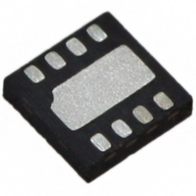
| 产品图片 |
|
| P1dB | 30.5dBm |
| 产品型号 | HMC409LP4E |
| RF类型 | WiMax |
| rohs | 无铅 / 符合限制有害物质指令(RoHS)规范要求 |
| 产品系列 | - |
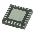
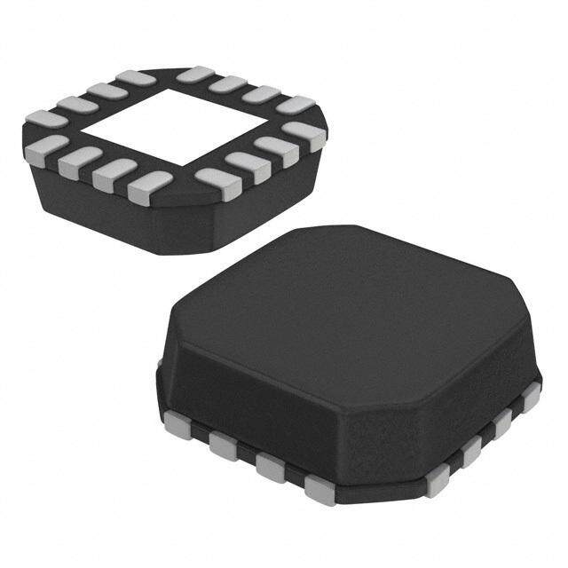
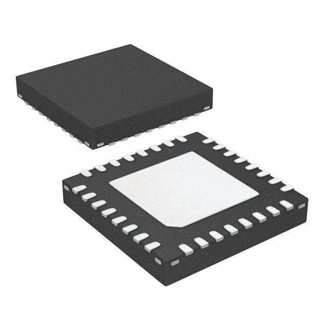
| 供应商器件封装 | 24-QFN(4x4) |
| 其它名称 | 1127-1371 |
| 包装 | 剪带 |
| 噪声系数 | 6dB |
| 增益 | 31dB |
| 封装/外壳 | 24-VFQFN 裸露焊盘 |
| 标准包装 | 100 |
| 测试频率 | - |
| 电压-电源 | 5V |
| 电流-电源 | 615mA |
| 频率 | 3.3GHz ~ 3.8GHz |


- 商务部:美国ITC正式对集成电路等产品启动337调查
- 曝三星4nm工艺存在良率问题 高通将骁龙8 Gen1或转产台积电
- 太阳诱电将投资9.5亿元在常州建新厂生产MLCC 预计2023年完工
- 英特尔发布欧洲新工厂建设计划 深化IDM 2.0 战略
- 台积电先进制程称霸业界 有大客户加持明年业绩稳了
- 达到5530亿美元!SIA预计今年全球半导体销售额将创下新高
- 英特尔拟将自动驾驶子公司Mobileye上市 估值或超500亿美元
- 三星加码芯片和SET,合并消费电子和移动部门,撤换高东真等 CEO
- 三星电子宣布重大人事变动 还合并消费电子和移动部门
- 海关总署:前11个月进口集成电路产品价值2.52万亿元 增长14.8%


PDF Datasheet 数据手册内容提取
HMC409LP4E v04.1217 GaAs InGaP HBT 1 WATT POWER AMPLIFIER, 3.3 - 3.8 GHz Typical Applications Features This amplifier is ideal for use as a power Gain: 31 dB T amplifier for 3.3 - 3.8 GHz applications: 40% pAe @ +32.5 dBm pout m • wimAX 802.16 2% eVm @ pout = +22 dBm s • fixed wireless Access with 54mbps ofDm signal - • wireless local loop +46 dBm output ip3 r integrated power Control (Vpd) e w Functional Diagram single +5V supply o General Description p The HmC409lp4e are high efficiency GaAs inGap & HBT mmiC power amplifiers operating from 3.3 to r 3.8 GHz. The amplifier is packaged in a low cost, A leadless smT package. Utilizing a minimum of e external components the amplifier provides 31 dB n of gain and +32.5 dBm of saturated power from a i l +5V supply voltage. The power control (Vpd) can be - used for full power down or rf output power/current s control. for +22 dBm ofDm output power (64 QAm, r 54 mbps), the HmC409lp4e achieve an error vector e magnitude (eVm) of 2%, meeting wimAX 802.16 lin- i f earity requirements. i l p m Electrical Specifications, T = +25° C, Vs = +5V, Vpd = +5V, Vbias=+5V A A parameter min. Typ. max. min. Typ. max. min. Typ. max. Units frequency range 3.3 - 3.4 3.4 - 3.6 3.6 - 3.8 GHz Gain 30 32 29 31.5 28 30 dB Gain Variation over Temperature 0.04 0.05 0.04 0.05 0.035 0.045 dB/ °C input return loss 10 15 15 dB output return loss 13 14 10 dB output power for 1dB Compression (p1dB) 28 30 28 30.5 28 30.5 dBm saturated output power (psat) 32 32.5 32 dBm output Third order intercept (ip3) [2] 41 45 42 45.5 41 45 dBm error Vector magnitude @ 3.5 GHz 2 % (54 mbps ofDm signal @ +22 dBm pout) noise figure 5.8 5.8 6 dB supply Current (icq) Vs= Vcc1 + Vcc2= +5V 615 615 615 mA Control Current (ipd) Vpd = +5V 4 4 4 mA switching speed ton, toff 20 20 20 ns Bias Current (ibias) 10 10 10 mA note 1: specifications and data reflect HmC409lp4e measured using the application circuit found herein. Contact the HmC Applications Group for assistance in optimizing performance for your application. note 2: Two-tone output power of +15 dBm per tone, 1 mHz spacing. Information furnished by Analog Devices is believed to be accurate and reliable. However, no For price, delivery, and to place orders: Analog Devices, Inc., responsibility is assumed by Analog Devices for its use, nor for any infringements of patents or other One Technology Way, P.O. Box 9106, Norwood, MA 02062-9106 1 rliicgehntss eo fi sth girrda nptaerdti ebsy t himatp mlicaayt iroens uolrt fortohme riwtsi sues eu.n Sdpeer caifinyc aptiaotnesn ts ourb jpeactte tnot crhigahntgs eo wf Aitnhaoluotg n oDteicveic. eNso. Phone: 781-329-4700 • Order online at www.analog.com Trademarks and registered trademarks are the property of their respective owners. Application Support: Phone: 1-800-ANALOG-D
HMC409LP4E v04.1217 GaAs InGaP HBT 1 WATT POWER AMPLIFIER, 3.3 - 3.8 GHz Broadband Gain & Return Loss Gain vs. Temperature 35 38 30 25 35 T 20 m NSE (dB) 11505 SSS212112 N (dB) 2392 - s SPO -05 GAI r RE -10 26 +25 C e --2105 23 +-4805 CC w -25 o -30 20 p 2 2.5 3 3.5 4 4.5 5 3 3.2 3.4 3.6 3.8 4 FREQUENCY (GHz) FREQUENCY (GHz) & r A Input Return Loss vs. Temperature Output Return Loss vs. Temperature e 0 0 n i l -5 +25 C -5 +85 C S (dB)-10 S (dB) -40 C s - S S-10 O O r RN L-15 RN L e U U-15 RET-20 ++2855 CC RET fi -40 C i -20 l -25 p -30 -25 m 3 3.2 3.4 3.6 3.8 4 3 3.2 3.4 3.6 3.8 4 A FREQUENCY (GHz) FREQUENCY (GHz) Reverse Isolation vs. Temperature Power Down Isolation vs. Temperature 0 0 -10 -10 dB)-20 ++2855 CC dB)-20 ++2855 CC N ( -40 C N ( -40 C O O TI-30 TI-30 A A L L O O IS-40 IS-40 -50 -50 -60 -60 3 3.2 3.4 3.6 3.8 4 3 3.2 3.4 3.6 3.8 4 FREQUENCY (GHz) FREQUENCY (GHz) For price, delivery, and to place orders: Analog Devices, Inc., One Technology Way, P.O. Box 9106, Norwood, MA 02062-9106 Phone: 781-329-4700 • Order online at www.analog.com 2 Application Support: Phone: 1-800-ANALOG-D
HMC409LP4E v04.1217 GaAs InGaP HBT 1 WATT POWER AMPLIFIER, 3.3 - 3.8 GHz P1dB vs. Temperature Psat vs. Temperature 36 36 T 34 34 m 32 32 s m) m) dB 30 dB 30 r - P1dB ( 28 PSAT ( 28 +25 C e +85 C 26 +25 C 26 -40 C w +85 C 24 -40 C 24 o p 22 22 3 3.2 3.4 3.6 3.8 4 3 3.1 3.2 3.3 3.4 3.5 3.6 3.7 3.8 3.9 4 & FREQUENCY (GHz) FREQUENCY (GHz) r A e Output IP3 vs. Temperature Power Compression @ 3.5 GHz n 50 40 i l %) 35 46 E ( - A 30 s B), P 25 r Bm) 42 N (d fie IP3 (d 38 ++-428055 CCC Bm), GAI 1250 d pli 34 Pout ( 150 GPPoaAuiEnt (((dd%BB))m) m 30 0 3 3.2 3.4 3.6 3.8 4 -20 -16 -12 -8 -4 0 4 8 A FREQUENCY (GHz) INPUT POWER (dBm) Gain & Power vs. Supply Voltage Noise Figure vs. Temperature 35 12 dBm) 34 10 ++2855 CC m), Psat ( 33 RE (dB) 8 -40 C B 32 U B (d FIG 6 B), P1d 3301 NOISE 4 d Gain AIN ( 29 PP1sdaBt 2 G 28 0 4.75 5 5.25 3 3.2 3.4 3.6 3.8 4 Vcc SUPPLY VOLTAGE (Vdc) FREQUENCY (GHz) For price, delivery, and to place orders: Analog Devices, Inc., One Technology Way, P.O. Box 9106, Norwood, MA 02062-9106 Phone: 781-329-4700 • Order online at www.analog.com 3 Application Support: Phone: 1-800-ANALOG-D
HMC409LP4E v04.1217 GaAs InGaP HBT 1 WATT POWER AMPLIFIER, 3.3 - 3.8 GHz Gain, Power & Quiescent Supply Current vs. Vpd @ 3.5 GHz Power Dissipation 40 800 4.4 m) 35 700 T sat (dB 30 600 N (W) 4 Max Pdiss @ +85C m P1dB (dBm), P 122505 Icc 345000000 Icc (mA) R DISSIPATIO 33..26 r - s AIN (dB), 150 PGP1sadainBt 120000 POWE 22..48 we G o 0 0 2 p 3 3.25 3.5 3.75 4 4.25 4.5 4.75 5 5.25 5.5 -20 -16 -12 -8 -4 0 4 8 Vpd (Vdc) INPUT POWER (dBm) & r EVM vs. Temperature @ 3.5 GHz OFDM A 54 Mbps Signal e 14 n E (%) 12 li D U - GNIT 10 ++2855 CC s MA 8 -40 C r R TO 6 e ROR VEC 4 lifi ER 2 p 0 m 10 12 14 16 18 20 22 24 26 28 30 A OUTPUT POWER (dBm) For price, delivery, and to place orders: Analog Devices, Inc., One Technology Way, P.O. Box 9106, Norwood, MA 02062-9106 Phone: 781-329-4700 • Order online at www.analog.com 4 Application Support: Phone: 1-800-ANALOG-D
HMC409LP4E v04.1217 GaAs InGaP HBT 1 WATT POWER AMPLIFIER, 3.3 - 3.8 GHz Typical Supply, Current vs. Supply Absolute Maximum Ratings Voltage, Vcc1 = Vcc2 = Vpd Collector Bias Voltage (Vcc1, Vcc2) +5.5 Vdc Vs (Vdc) icq (mA) T Control Voltage (Vpd) +5.5 Vdc 4.75 516 m rf input power (rfin)(Vs = Vpd = +5Vdc) +10 dBm 5.0 615 s Junction Temperature 150 °C 5.25 721 Continuous pdiss (T = 85 °C) - 3.74 w (derate 57.5 mw/°C above 85 °C) r Thermal resistance e 17.4 °C/w (junction to ground paddle) w storage Temperature -65 to +150 °C eleCTrosTATiC sensiTiVe DeViCe o operating Temperature -40 to +85 °C oBserVe HAnDlinG preCAUTions p Class 1A, esD sensitivity (HBm) & 24-Lpeaasdse Lde 2a5d0 FVrame Chip Scale Package [LFCSP] Outline Drawing 4 x 4 mm Body and 0.85 mm Package Height (CP-24-16) r Dimensions shown in millimeters A DETAIL A e (JEDEC 95) n 4.10 0.30 i 4.00 SQ 0.25 l PIN 1 3.90 0.18 PIN 1 INDICATOR INDICATOR AREA OPTIONS - 19 24 (SEE DETAIL A) s 18 1 r 0.50 BSC 2.85 e EXPOSED 2.70 SQ PAD i 2.55 f i 13 6 l 0.50 12 7 0.20 MIN p TOP VIEW BOTTOM VIEW 0.40 m 0.30 FOR PROPER CONNECTION OF A 0.90 THE EXPOSED PAD, REFER TO 0.85 THE PIN CONFIGURATION AND 0.80 0.05 MAX FUNCTION DESCRIPTIONS 0.02 NOM SECTION OF THIS DATA SHEET. COPLANARITY PKG-004926/PKG-004942 SEPALTAINNGE COMPLIANT TO JEDE0C.2 S0 TRAENFDAR0D.0S8 MO-220-VGGD-8. 05-25-2016-B 24-lead lead frame Chip scale package [lfCsp] 4 mm × 4 mm Body and 0.85 mm package Height (Cp-24-16) Dimensions shown in millimeters. Package Information part number package Body material lead finish msl rating package marking [2] HmC409lp4e roHs-compliant low stress injection molded plastic 100% matte sn msl3 [1] H409 XXXX [1] max peak reflow temperature of 260 °C [2] 4-Digit lot number XXXX For price, delivery, and to place orders: Analog Devices, Inc., One Technology Way, P.O. Box 9106, Norwood, MA 02062-9106 Phone: 781-329-4700 • Order online at www.analog.com 5 Application Support: Phone: 1-800-ANALOG-D
HMC409LP4E v04.1217 GaAs InGaP HBT 1 WATT POWER AMPLIFIER, 3.3 - 3.8 GHz Application Circuit T m s - r e w o p & E r A e n i l - s r e i f i l p m A recommended Component Values Tl1 Tl2 Tl3 C1 - C5 100 pf impedance 50 ohm 27 ohm 50 ohm C6 - C7 1000 pf physical length 0.068” 0.062” 0.164” C8 10 pf electrical length 12˚ 11˚ 29˚ C9 0.5 pf pCB material: 10 mil rogers 4350, er = 3.48 C10 1.6 pf C11 4.7µf l1, l2 3.9 nH l3 2.2 nH r1 56 ohm For price, delivery, and to place orders: Analog Devices, Inc., One Technology Way, P.O. Box 9106, Norwood, MA 02062-9106 Phone: 781-329-4700 • Order online at www.analog.com 6 Application Support: Phone: 1-800-ANALOG-D
HMC409LP4E v04.1217 GaAs InGaP HBT 1 WATT POWER AMPLIFIER, 3.3 - 3.8 GHz Pin Descriptions pin number function Description interface schematic T 1-3, 5, 6, 8, 10 -14, no connection required. These pins may be connected to m n/C 18, 19, 21, 22, 24 rf/DC ground without affecting performance. s This pin is AC coupled 4 rfin - and matched to 50 ohms. r e w power control pin. for maximum power, this pin should be connected to 5V thru a 56 Ω resistor. A high-voltage or 7 Vpd o small resistor is not recommended for lower idle current. This voltage can be reduced or the resistor increased. p & r A 9 Vbias DC power supply pin for bias circuitry e n i l - s 15, 16, 17 rfoUT rf output and DC bias for the output stage. r e i f power supply voltage for the second amplifier stage. i 20 Vcc2 external bypass capacitors and pull up choke are required l as shown in the application schematic. p m power supply voltage for the first amplifier stage. external A 23 Vcc1 bypass capacitors are required as shown in the application schematic. Ground: Backside of package has exposed metal ground GnD slug that must be connected to ground thru a short path. Vias under the device are required. For price, delivery, and to place orders: Analog Devices, Inc., One Technology Way, P.O. Box 9106, Norwood, MA 02062-9106 Phone: 781-329-4700 • Order online at www.analog.com 7 Application Support: Phone: 1-800-ANALOG-D
HMC409LP4E v04.1217 GaAs InGaP HBT 1 WATT POWER AMPLIFIER, 3.3 - 3.8 GHz Evaluation PCB T m s - r e w o p & r A e n i l - s r e i f i l p m A List of Materials for Evaluation PCB 108355 [1] The circuit board used in the application should item Description use rf circuit design techniques. signal lines should J1 - J2 pCB mount smA rf Connector have 50 ohm impedance while the package ground J3, J4 2 mm DC Header leads and exposed paddle should be connected C1 - C5 100 pf Capacitor, 0402 pkg. directly to the ground plane similar to that shown. C6 - C7 1000 pf Capacitor, 0603 pkg. A sufficient number of via holes should be used C8 10 pf Capacitor, 0402 pkg. to connect the top and bottom ground planes. The C9 0.5 pf Capacitor, 0603 pkg. evaluation board should be mounted to an appropri- C10 1.6 pf Capacitor, 0603 pkg. ate heat sink. The evaluation circuit board shown is C11 4.7 µf, Tantalum available from Analog Devices, upon request. l1, l2 3.9 nH inductor, 0603 pkg. l3 2.2 nH inductor, 0402 pkg. Toko r1 56 ohm resistor, 0603 pkg. U1 HmC409lp4e Amplifier pCB [2] 108353 eval Board [1] reference this number when ordering complete evaluation pCB [2] Circuit Board material: rogers 4350, er = 3.48 For price, delivery, and to place orders: Analog Devices, Inc., One Technology Way, P.O. Box 9106, Norwood, MA 02062-9106 Phone: 781-329-4700 • Order online at www.analog.com 8 Application Support: Phone: 1-800-ANALOG-D
Mouser Electronics Authorized Distributor Click to View Pricing, Inventory, Delivery & Lifecycle Information: A nalog Devices Inc.: HMC409LP4E HMC409LP4ETR 108355-HMC409LP4