ICGOO在线商城 > 分立半导体产品 > 晶体管 - 双极 (BJT) - 单 > 2DA1213Y-13

 Datasheet下载
- 型号: 2DA1213Y-13
- 制造商: Diodes Inc.
- 库位|库存: xxxx|xxxx
- 要求:
| 数量阶梯 | 香港交货 | 国内含税 |
| +xxxx | $xxxx | ¥xxxx |
查看当月历史价格
查看今年历史价格
2DA1213Y-13产品简介:
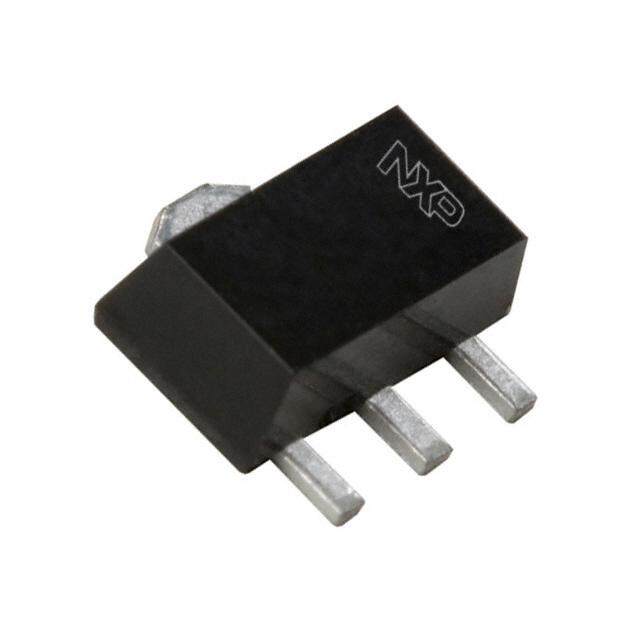
ICGOO电子元器件商城为您提供2DA1213Y-13由Diodes Inc.设计生产,在icgoo商城现货销售,并且可以通过原厂、代理商等渠道进行代购。 2DA1213Y-13价格参考。Diodes Inc.2DA1213Y-13封装/规格:晶体管 - 双极 (BJT) - 单, 双极 (BJT) 晶体管 PNP 50V 2A 160MHz 1W 表面贴装 SOT-89-3。您可以下载2DA1213Y-13参考资料、Datasheet数据手册功能说明书,资料中有2DA1213Y-13 详细功能的应用电路图电压和使用方法及教程。
Diodes Incorporated 的 2DA1213Y-13 是一款双极型晶体管(BJT),属于单晶体管类别。该型号广泛应用于多种电子电路中,以下是其主要应用场景:

 1. 开关应用
   - 电源管理:用于简单的开关电路中,控制负载的通断,例如 LED 驱动、继电器驱动等。
   - 数字电路接口:在需要将低电平信号转换为高电平信号或驱动较大负载时,作为开关元件使用。

 2. 放大应用
   - 音频信号放大:适用于小型音频设备中的前置放大或中频信号放大。
   - 传感器信号放大:将微弱的传感器信号放大到可被后续电路处理的水平。
   - 射频(RF)应用:在低功率射频电路中,用作信号放大器。

 3. 保护电路
   - 过流保护:通过设计限流电路,防止后级电路因过载而损坏。
   - 反向电压保护:在某些情况下,可以用作防止电源极性接反的保护元件。

 4. 稳压电路
   - 在简易线性稳压器中,作为调整管使用,配合分压电阻和稳压二极管实现输出电压的稳定。

 5. 电机驱动
   - 用于小功率直流电机的启动、停止和速度控制,适合低功耗场景。

 6. 通信设备
   - 在低功率无线通信模块中,用作信号调制或解调的放大元件。

 注意事项:
- 2DA1213Y-13 的具体参数(如电流、电压和频率范围)决定了其适用范围,请根据实际需求选择合适的偏置条件和外围电路。
- 在高频或大功率场景下,需注意散热设计和寄生电容的影响。

总结来说,2DA1213Y-13 适用于低功率、通用型的开关和放大场景,广泛应用于消费电子、工业控制和通信领域。
| 参数 | 数值 |
| 产品目录 | |
| 描述 | TRANS PNP MED BIPO 50V SOT89-3两极晶体管 - BJT 1W -50V |
| 产品分类 | 晶体管(BJT) - 单路分离式半导体 |
| 品牌 | Diodes Incorporated |
| 产品手册 | |
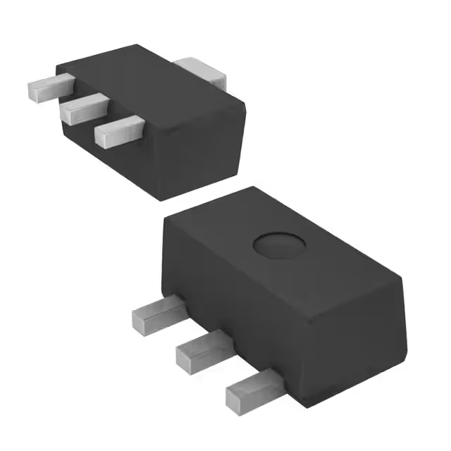
| 产品图片 |
|
| rohs | 符合RoHS无铅 / 符合限制有害物质指令(RoHS)规范要求 |
| 产品系列 | 晶体管,两极晶体管 - BJT,Diodes Incorporated 2DA1213Y-13- |
| 数据手册 | |
| 产品型号 | 2DA1213Y-13 |
| PCN其它 | |
| RoHS指令信息 | http://diodes.com/download/4349 |
| 不同 Ib、Ic时的 Vce饱和值(最大值) | 500mV @ 50mA,1A |
| 不同 Ic、Vce 时的DC电流增益(hFE)(最小值) | 120 @ 500mA,2V |
| 产品目录页面 | |
| 产品种类 | 两极晶体管 - BJT |
| 供应商器件封装 | SOT-89-3 |
| 其它名称 | 2DA1213Y-13-ND |
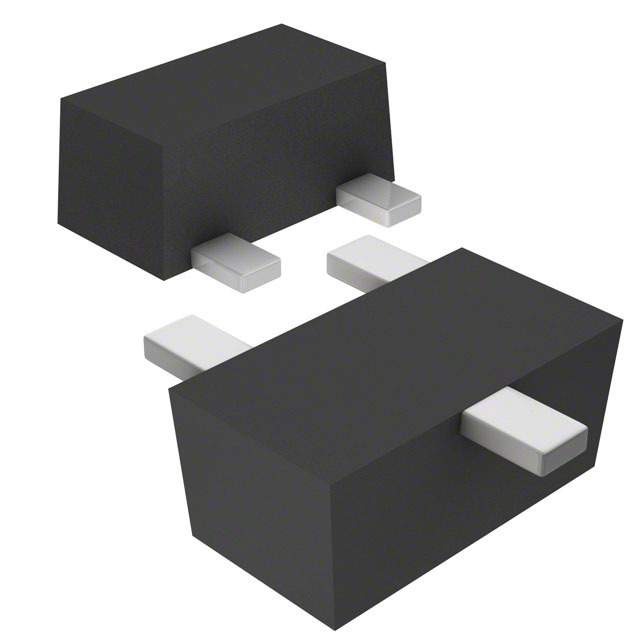
| 其它图纸 |
|
| 功率-最大值 | 1W |
| 包装 | 带卷 (TR) |
| 发射极-基极电压VEBO | 5 V |
| 商标 | Diodes Incorporated |
| 增益带宽产品fT | 160 MHz |
| 安装类型 | 表面贴装 |
| 安装风格 | SMD/SMT |
| 封装 | Reel |
| 封装/外壳 | TO-243AA |
| 封装/箱体 | SOT-89 |
| 工厂包装数量 | 2500 |
| 晶体管极性 | PNP |
| 晶体管类型 | PNP |
| 最大功率耗散 | 1000 mW |
| 最大工作温度 | + 150 C |
| 最大直流电集电极电流 | 2 A |
| 最小工作温度 | - 55 C |
| 标准包装 | 2,500 |
| 电压-集射极击穿(最大值) | 50V |
| 电流-集电极(Ic)(最大值) | 2A |
| 电流-集电极截止(最大值) | - |
| 直流电流增益hFE最大值 | 120 at 0.5 A at 2 V |
| 直流集电极/BaseGainhfeMin | 120 |
| 系列 | 2DA1213 |
| 配置 | Single |
| 集电极—发射极最大电压VCEO | 50 V |
| 集电极—基极电压VCBO | 50 V |
| 频率-跃迁 | 160MHz |


- 商务部:美国ITC正式对集成电路等产品启动337调查
- 曝三星4nm工艺存在良率问题 高通将骁龙8 Gen1或转产台积电
- 太阳诱电将投资9.5亿元在常州建新厂生产MLCC 预计2023年完工
- 英特尔发布欧洲新工厂建设计划 深化IDM 2.0 战略
- 台积电先进制程称霸业界 有大客户加持明年业绩稳了
- 达到5530亿美元!SIA预计今年全球半导体销售额将创下新高
- 英特尔拟将自动驾驶子公司Mobileye上市 估值或超500亿美元
- 三星加码芯片和SET,合并消费电子和移动部门,撤换高东真等 CEO
- 三星电子宣布重大人事变动 还合并消费电子和移动部门
- 海关总署:前11个月进口集成电路产品价值2.52万亿元 增长14.8%


PDF Datasheet 数据手册内容提取
2DA1213O/Y 50V PNP POWER SWITCHING TRANSISTOR IN SOT89 Features Mechanical Data BVCEO > -50V Case: SOT89 IC = -2A high Continuous Collector Current Case material: Molded Plastic. “Green” Molding Compound. High Gain Holds up UL Flammability Rating 94V-0 Totally Lead-Free & Fully RoHS compliant (Notes 1 & 2) Moisture Sensitivity: Level 1 per J-STD-020 Halogen and Antimony Free. “Green” Device (Note 3) Terminals: Finish - Matte Tin Plated Leads, Solderable per Qualified to AEC-Q101 Standards for High Reliability MIL-STD-202, Method 208 Weight: 0.052 grams (Approximate) SOT89 C E B C C B E Top View Top View Device Symbol Pin Out Ordering Information (Notes 4) Product Marking Reel size (inches) Tape width (mm) Quantity per reel 2DA1213O-13 P25X 13 12 2,500 2DA1213Y-13 P25Y 13 12 2,500 2DA1213Y-13R P25Y 13 12 4,000 Notes: 1. No purposely added lead. Fully EU Directive 2002/95/EC (RoHS) & 2011/65/EU (RoHS 2) compliant. 2. See http://www.diodes.com/quality/lead_free.html for more information about Diodes Incorporated’s definitions of Halogen- and Antimony-free, "Green" and Lead-free. 3. Halogen- and Antimony-free "Green” products are defined as those which contain <900ppm bromine, <900ppm chlorine (<1500ppm total Br + Cl) and <1000ppm antimony compounds. 4. For packaging details, go to our website at http”//www.diodes.com/products/packages.html Marking Information xxxx = Product Type Marking Code: P25X = 2DA1213O YWW P25Y = 2DA1213Y xxxx YWW = Date Code Marking Y = Last digit of year (ex: 1 = 2011) WW = Week code 01 - 53 2DA1213O/Y 1 of 6 February 2013 Document number: DS31306 Rev: 5 - 2 www.diodes.com © Diodes Incorporated
2DA1213O/Y Maximum Ratings (@TA = +25°C, unless otherwise specified.) Characteristic Symbol Value Unit Collector-Base Voltage VCBO -50 V Collector-Emitter Voltage VCEO -50 V Emitter-Base Voltage VEBO -6 V Continuous Collector Current IC -2 A Peak Pulse Current ICM -2.5 A Base Current IB -500 mA Thermal Characteristics (@TA = +25°C, unless otherwise specified.) Characteristic Symbol Value Unit Power Dissipation (Note 5) PD 1 W Thermal Resistance, Junction to Ambient (Note 5) RθJA 125 C/W Thermal Resistance, Junction to Leads (Note 6) RθJL 18.3 C/W Operating and Storage Temperature Range TJ, TSTG -55 to +150 C Notes: 5. For a device surface mounted on 15mm x 15mm x 0.6mm FR4 PCB with high coverage of single sided 1 oz copper, in still air conditions; the device is measured when operating in steady state condition. 6. Thermal resistance from junction to solder-point (on the exposed collector pad). Thermal Characteristics and Derating Information W) 1.0 W) 120 n ( 0.8 C/ 100 atio e (° 80 p 0.6 c D=0.5 si an 60 er Dis 0.4 Resist 40 D=0.2 Single Pulse ow 0.2 al 20 D=0.05 Max P 0.00 25 50 75 100 125 150 herm 1000µ 1m 10m 100m D1=0.1 10 100 1k Temperature (°C) T Pulse Width (s) Derating Curve Transient Thermal Impedance 100 ) Single Pulse. T =25°C W amb ( n o ati p 10 si s Di r e w o P x 1 Ma 100µ 1m 10m 100m 1 10 100 1k Pulse Width (s) Pulse Power Dissipation 2DA1213O/Y 2 of 6 February 2013 Document number: DS31306 Rev: 5 - 2 www.diodes.com © Diodes Incorporated
2DA1213O/Y Electrical Characteristics (@TA = +25°C, unless otherwise specified.) Characteristic Symbol Min Typ Max Unit Test Condition Collector-Base Breakdown Voltage BVCBO -50 — — V IC = -100µA Collector-Emitter Breakdown Voltage (Note 7) BVCEO -50 — — V IC = -10mA Emitter-Base Breakdown Voltage BVEBO -6 — — V IE = -100µA Collector Cut-off Current ICBO — — -100 nA VCB = -50V Emitter Cut-off Current IEBO — — -100 nA VEB = -5V 2DA1213O 70 140 IC = -500mA, VCE = -2V DC Current Gain (Note 8) 2DA1213Y hFE 120 — 240 — IC = -500mA, VCE = -2V 2DA1213O, 2DA1213Y 20 — IC = -2A, VCE = -2V Collector-Emitter Saturation Voltage (Note 7) VCE(sat) — — -0.5 V IC = -1A, IB = -50mA Base-Emitter Turn-On Voltage (Note 7) VBE(sat) — — -1.2 V IC = -1A, IB = -50mA Transition Frequency fT — 160 — MHz IfC = = 1 -0100M0HmzA , VCE = -2V, Output Capacitance Cobo — 17 — pF VCB = -10V, IE = 0, f = 1MHz Turn-On Time ton — 25 — ns SFatollr aTgime eT ime tt((sf)) —— 11320 —— nnss VIBC1 E== --I2B2V ,= I C-5 =0 m-1AA , Note: 7. Measured under pulsed conditions. Pulse width ≤ 300µs. Duty cycle ≤ 2%. Typical Electrical Characteristics (@TA = +25°C, unless otherwise specified.) 1.0 200 IB = -10mA TA = 150°C VCE = -2V A) 0.8 ENT ( IB = -8mA AIN 150 TA = 85°C R G UR 0.6 NT C IB = -6mA E OR RR 100 TA = 25°C CT CU LE 0.4 IB = -4mA DC OL , E -I, CC 0.2 IB = -2mA hF 50 TA = -55°C 0 0 0 1 2 3 4 5 0.001 0.01 0.1 1 10 -V , COLLECTOR-EMITTER VOLTAGE (V) -I , COLLECTOR CURRENT (A) CE C Figure 1 Typical Collector Current vs. Collector-Emitter Voltage Figure 2 Typical DC Current Gain vs. Collector Current (2DA1213O) 2DA1213O/Y 3 of 6 February 2013 Document number: DS31306 Rev: 5 - 2 www.diodes.com © Diodes Incorporated
2DA1213O/Y 1 V) 1.2 E ( G VCE = -2V A R IC/IB = 20 LT 1 E O TV) V LLECTOR-EMITON VOLTAGE ( 0.1 TA = 85°C TA = 150°C TER TURN-ON 00..68 TTAA == 2-55°5C°C OTI T CA MI -V, CE(SAT)SATUR TA = -55°C TA = 25°C , BASE-EN)00..24 TTAA == 8155°0C°C O E( B 0.01 V 0 0.0001 0.001 0.01 0.1 1 10 - 0.0001 0.001 0.01 0.1 1 10 -IC, COLLECTOR CURRENT (A) -IC, COLLECTOR CURRENT (A) Figure 3 Typical Collector-Emitter Saturation Voltage Figure 4 Typical Base-Emitter Turn-On Voltage vs. Collector Current vs. Collector Current V) 1.2 60 E ( IC/IB = 20 G TA 1.0 F) f = 1MHz L p VO E ( 45 ON 0.8 ANC TI T RA TA = -55°C ACI U P T 0.6 A 30 A C R S TA = 25°C UT E P T 0.4 T MIT TA = 85°C OU SE-E 0.2 TA = 150°C C, obo15 A B , T) SA 0 0 E( 0.0001 0.001 0.01 0.1 1 10 0.01 0.1 1 10 100 B V - -IC, COLLECTOR CURRENT (A) VR, REVERSE VOLTAGE (V) Figure 5 Typical Base-Emitter Saturation Voltage Figure 6 Typical Output Capacitance Characteristics vs. Collector Current z)200 H M T ( C U D150 O R P H T D WI100 D N A B N- AI G 50 VCE = -6V T f = 100MHz N E R R U C 0 , T 0 10 20 30 40 50 60 70 80 90 100 f -I , COLLECTOR CURRENT (mA) C Figure 7 Typical Gain-Bandwidth Product vs. Collector Current 2DA1213O/Y 4 of 6 February 2013 Document number: DS31306 Rev: 5 - 2 www.diodes.com © Diodes Incorporated
2DA1213O/Y Package Outline Dimensions Please see AP02002 at http://www.diodes.com/datasheets/ap02002.pdf for latest version. D1 R 0.200 C SOT89 Dim Min Max H1 H A 1.40 1.60 E B 0.44 0.62 B1 0.35 0.54 C 0.35 0.44 B1 B L D 4.40 4.60 D1 1.62 1.83 e E 2.29 2.60 8° (4X) e 1.50 Typ H 3.94 4.25 H1 2.63 2.93 A L 0.89 1.20 All Dimensions in mm D Suggested Pad Layout Please see AP02001 at http://www.diodes.com/datasheets/ap02001.pdf for the latest version. X1 Dimensions Value (in mm) X 0.900 X2 (2x) X1 1.733 Y1 X2 0.416 Y3 Y4 Y 1.300 Y1 4.600 Y Y2 Y2 1.475 Y3 0.950 C Y4 1.125 C 1.500 X (3x) 2DA1213O/Y 5 of 6 February 2013 Document number: DS31306 Rev: 5 - 2 www.diodes.com © Diodes Incorporated
2DA1213O/Y IMPORTANT NOTICE DIODES INCORPORATED MAKES NO WARRANTY OF ANY KIND, EXPRESS OR IMPLIED, WITH REGARDS TO THIS DOCUMENT, INCLUDING, BUT NOT LIMITED TO, THE IMPLIED WARRANTIES OF MERCHANTABILITY AND FITNESS FOR A PARTICULAR PURPOSE (AND THEIR EQUIVALENTS UNDER THE LAWS OF ANY JURISDICTION). Diodes Incorporated and its subsidiaries reserve the right to make modifications, enhancements, improvements, corrections or other changes without further notice to this document and any product described herein. Diodes Incorporated does not assume any liability arising out of the application or use of this document or any product described herein; neither does Diodes Incorporated convey any license under its patent or trademark rights, nor the rights of others. Any Customer or user of this document or products described herein in such applications shall assume all risks of such use and will agree to hold Diodes Incorporated and all the companies whose products are represented on Diodes Incorporated website, harmless against all damages. Diodes Incorporated does not warrant or accept any liability whatsoever in respect of any products purchased through unauthorized sales channel. Should Customers purchase or use Diodes Incorporated products for any unintended or unauthorized application, Customers shall indemnify and hold Diodes Incorporated and its representatives harmless against all claims, damages, expenses, and attorney fees arising out of, directly or indirectly, any claim of personal injury or death associated with such unintended or unauthorized application. Products described herein may be covered by one or more United States, international or foreign patents pending. Product names and markings noted herein may also be covered by one or more United States, international or foreign trademarks. This document is written in English but may be translated into multiple languages for reference. Only the English version of this document is the final and determinative format released by Diodes Incorporated. LIFE SUPPORT Diodes Incorporated products are specifically not authorized for use as critical components in life support devices or systems without the express written approval of the Chief Executive Officer of Diodes Incorporated. As used herein: A. Life support devices or systems are devices or systems which: 1. are intended to implant into the body, or 2. support or sustain life and whose failure to perform when properly used in accordance with instructions for use provided in the labeling can be reasonably expected to result in significant injury to the user. B. A critical component is any component in a life support device or system whose failure to perform can be reasonably expected to cause the failure of the life support device or to affect its safety or effectiveness. Customers represent that they have all necessary expertise in the safety and regulatory ramifications of their life support devices or systems, and acknowledge and agree that they are solely responsible for all legal, regulatory and safety-related requirements concerning their products and any use of Diodes Incorporated products in such safety-critical, life support devices or systems, notwithstanding any devices- or systems-related information or support that may be provided by Diodes Incorporated. Further, Customers must fully indemnify Diodes Incorporated and its representatives against any damages arising out of the use of Diodes Incorporated products in such safety-critical, life support devices or systems. Copyright © 2013, Diodes Incorporated www.diodes.com 2DA1213O/Y 6 of 6 February 2013 Document number: DS31306 Rev: 5 - 2 www.diodes.com © Diodes Incorporated