ICGOO在线商城 > 分立半导体产品 > 晶体管 - 双极 (BJT) - 单 > 2SD1803S-E
 Datasheet下载
- 型号: 2SD1803S-E
- 制造商: ON Semiconductor
- 库位|库存: xxxx|xxxx
- 要求:
| 数量阶梯 | 香港交货 | 国内含税 |
| +xxxx | $xxxx | ¥xxxx |
查看当月历史价格
查看今年历史价格
2SD1803S-E产品简介:
ICGOO电子元器件商城为您提供2SD1803S-E由ON Semiconductor设计生产,在icgoo商城现货销售,并且可以通过原厂、代理商等渠道进行代购。 2SD1803S-E价格参考¥0.40-¥0.40。ON Semiconductor2SD1803S-E封装/规格:晶体管 - 双极 (BJT) - 单, 双极 (BJT) 晶体管 NPN 50V 5A 180MHz 1W 通孔 TP。您可以下载2SD1803S-E参考资料、Datasheet数据手册功能说明书,资料中有2SD1803S-E 详细功能的应用电路图电压和使用方法及教程。
ON Semiconductor 的2SD1803S-E是一款双极型晶体管(BJT),广泛应用于需要高效、稳定电流放大的电路中。其具体应用场景包括但不限于以下几个方面:

 1. 音频放大器
   2SD1803S-E 可用于音频信号的放大,尤其是在功率放大级。它能够提供足够的增益和电流驱动能力,确保音频信号在不失真的情况下被放大,适用于音响设备、耳机放大器等。

 2. 开关电源
   在开关电源设计中,2SD1803S-E可以作为开关元件使用。它能够快速响应电压变化,确保电源输出的稳定性。由于其低饱和电压和高电流处理能力,适合用于DC-DC转换器、线性稳压器等场合。

 3. 电机驱动
   该晶体管可用于小型电机的驱动控制。通过调节基极电流,可以实现对电机转速和方向的精确控制。其较高的电流承受能力和良好的散热性能,使其在电机驱动电路中表现出色。

 4. 信号调理电路
   在工业自动化、传感器信号处理等领域,2SD1803S-E可以用于信号调理电路中。它可以将微弱的输入信号进行放大,并且具有较好的线性度,确保信号不失真地传输到后续处理单元。

 5. 保护电路
   2SD1803S-E还可以用于过流保护、短路保护等电路中。通过检测电流的变化,当电流超过设定值时,晶体管可以迅速切断电路,防止损坏其他元器件。

 6. 脉宽调制(PWM)控制
   在PWM控制电路中,2SD1803S-E可以用作开关元件,根据PWM信号的占空比来调节输出功率。这种应用常见于LED驱动、风扇速度控制等场合。

 总结
2SD1803S-E凭借其优良的电气特性,如高增益、低饱和电压和较大的电流处理能力,适合应用于多种需要电流放大的场合。无论是音频放大、电源管理还是电机驱动,它都能提供可靠的性能表现。
| 参数 | 数值 |
| 产品目录 | |
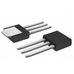
| 描述 | TRANS NPN HI CURRENT SW TP两极晶体管 - BJT LOW-SATURATION VOLTAGE |
| 产品分类 | 晶体管(BJT) - 单路分离式半导体 |
| 品牌 | ON Semiconductor |
| 产品手册 | |
| 产品图片 |
|
| rohs | 符合RoHS无铅 / 符合限制有害物质指令(RoHS)规范要求 |
| 产品系列 | 晶体管,两极晶体管 - BJT,ON Semiconductor 2SD1803S-E- |
| 数据手册 | |
| 产品型号 | 2SD1803S-E |
| 不同 Ib、Ic时的 Vce饱和值(最大值) | 400mV @ 150mA,3A |
| 不同 Ic、Vce 时的DC电流增益(hFE)(最小值) | 140 @ 500mA,2V |
| 产品种类 | 两极晶体管 - BJT |
| 供应商器件封装 | TP |
| 功率-最大值 | 1W |
| 包装 | 散装 |
| 发射极-基极电压VEBO | 6 V |
| 商标 | ON Semiconductor |
| 增益带宽产品fT | 180 MHz |
| 安装类型 | 通孔 |
| 安装风格 | Through Hole |
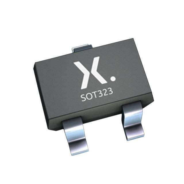
| 封装/外壳 | TO-251-3 短引线,IPak,TO-251AA |
| 封装/箱体 | DPAK |
| 工厂包装数量 | 500 |
| 晶体管极性 | NPN/PNP |
| 晶体管类型 | NPN |
| 最大功率耗散 | 1 W |
| 标准包装 | 500 |
| 电压-集射极击穿(最大值) | 50V |
| 电流-集电极(Ic)(最大值) | 5A |
| 电流-集电极截止(最大值) | - |
| 直流集电极/BaseGainhfeMin | 55 |
| 系列 | 2SD1803 |
| 集电极—发射极最大电压VCEO | 50 V |
| 集电极连续电流 | 5 A |
| 频率-跃迁 | 180MHz |


- 商务部:美国ITC正式对集成电路等产品启动337调查
- 曝三星4nm工艺存在良率问题 高通将骁龙8 Gen1或转产台积电
- 太阳诱电将投资9.5亿元在常州建新厂生产MLCC 预计2023年完工
- 英特尔发布欧洲新工厂建设计划 深化IDM 2.0 战略
- 台积电先进制程称霸业界 有大客户加持明年业绩稳了
- 达到5530亿美元!SIA预计今年全球半导体销售额将创下新高
- 英特尔拟将自动驾驶子公司Mobileye上市 估值或超500亿美元
- 三星加码芯片和SET,合并消费电子和移动部门,撤换高东真等 CEO
- 三星电子宣布重大人事变动 还合并消费电子和移动部门
- 海关总署:前11个月进口集成电路产品价值2.52万亿元 增长14.8%


PDF Datasheet 数据手册内容提取
Ordering number : EN2085C 2SB1203/2SD1803 Bipolar Transistor (–)50V, (–)5A, Low VCE(sat), (PNP)NPN Single TP/TP-FA http://onsemi.com Applications • Relay drivers, high-speed inverters, converters, and other general high-current switching applications Features • Low collector-to-emitter saturation voltage • High current and high fT • Excellent linearity of hFE • Fast switching speed • Small and slim package making it easy to make 2SB1203/2SD1803-applied sets smaller Specifi cations ( ): 2SB1203 Absolute Maximum Ratings at Ta=25°C Parameter Symbol Conditions Ratings Unit Collector-to-Base Voltage VCBO (--)60 V Collector-to-Emitter Voltage VCEO (--)50 V Emitter-to-Base Voltage VEBO (--)6 V Collector Current IC (--)5 A Collector Current (Pulse) ICP (--)8 A Continued on next page. Package Dimensions unit : mm (typ) Package Dimensions unit : mm (typ) 7518-003 7003-003 6.5 2.3 6.5 2.3 5.0 0.5 2SB1203S-E 5.0 0.5 2SB1203S-TL-E 4 1.5 2SB1203S-H 4 1.5 2SB1203S-Tl-H 2SD1203T-E 2SB1203T-TL-E 2SD1203T-H 2SB1203T-Tl-H 5.5 7.0 2SB1803S-E 5.5 7.0 2SB1803S-TL-E 2SB1803S-H 2SB1803S-Tl-H 0.85 2SD1803T-E 0.85 0.5 2 2SB1803T-TL-E 0.7 1. 1.2 2SD1803T-H 8 2.5 2SB1803T-Tl-H 0.81.6 5 1 20. 3 0.6 7. 0.5 0.6 0 to 0.2 1 : Base 1 : Base 1.2 2 : Collector 2 : Collector 1 2 3 3 : Emitter 3 : Emitter 4 : Collector 4 : Collector 2.3 2.3 TP-FA 2.3 2.3 TP Product & Package Information • Package : TP • Package : TP-FA • JEITA, JEDEC : SC-64, TO-251 • JEITA, JEDEC : SC-63, TO-252 • Minimum Packing Quantity : 500 pcs./bag • Minimum Packing Quantity : 700 pcs./reel Marking Packing Type (TP-FA) : TL Electrical Connection (TP, TP-FA) 2,4 2,4 B1203 D1803 1 1 RANK LOT No. RANK LOT No. TL 2SB1203 3 2SD1803 3 Semiconductor Components Industries, LLC, 2013 September, 2013 60612EA TKIM TA-4030, TA-4052/N2503TN (KT)/92098HA (KT)/8309MO/3097AT, TS No.2085-1/10
2SB1203 / 2SD1803 Continued from preceding page. Parameter Symbol Conditions Ratings Unit 1 W Collector Dissipation PC Tc=25°C 20 W Junction Temperature Tj 150 °C Storage Temperature Tstg --55 to +150 °C Stresses exceeding Maximum Ratings may damage the device. Maximum Ratings are stress ratings only. Functional operation above the Recommended Operating Conditions is not implied. Extended exposure to stresses above the Recommended Operating Conditions may affect device reliability. Electrical Characteristics at Ta=25°C Ratings Parameter Symbol Conditions Unit min typ max Collector Cutoff Current ICBO VCB=(--)40V, IE=0A (--)1 μA Emitter Cutoff Current IEBO VEB=(--)4V, IC=0A (--)1 μA hFE1 VCE=(--)2V, IC=(--)0.5A 70* 400* DC Current Gain hFE2 VCE=(--)2V, IC=(--)4A 35 Gain-Bandwidth Product fT VCE=(--)5V, IC=(--)1A (130)180 MHz Output Capacitance Cob VCB=(--)10V, f=1MHz (60)40 pF Collector-to-Emitter Saturation Voltage VCE(sat) IC=(--)3A, IB=(--)0.15A (--280)220 (--550)400 mV Base-to-Emitter Saturation Voltage VBE(sat) IC=(--)3A, IB=(--)0.15A (--)0.95 (--)1.3 V Collector-to-Base Breakdown Voltage V(BR)CBO IC=(--)10μA, IE=0A (--)60 V Collector-to-Emitter Breakdown Voltage V(BR)CEO IC=(--)1mA, RBE=∞ (--)50 V Emitter-to-Base Breakdown Voltage V(BR)EBO IE=(--)10μA, IC=0A (--)6 V Turn-On Time ton (50)50 ns Storage Time tstg See specifi ed Test Circuit. (450)500 ns Fall Time tf (20)20 ns * : The 2SB1203/2SD1803 are classifi ed by 0.5A hFE as follows : Rank Q R S T hFE 70 to 140 100 to 200 140 to 280 200 to 400 Switching Time Test Circuit IB1 PW=20(cid:77)s OUTPUT D.C.(cid:98)1% IB2 INPUT VR RB RL 50(cid:55) + + 100(cid:77)F 470(cid:77)F VBE= --5V VCC=25V IC=10IB1= --10IB2=2A For PNP, the polarity is reversed. Ordering Information Device Package Shipping memo 2SB1203S-E TP 500pcs./bag Pb Free 2SB1203S-H TP 500pcs./bag Pb Free and Halogen Free 2SD1203T-E TP 500pcs./bag Pb Free 2SD1203T-H TP 500pcs./bag Pb Free and Halogen Free 2SB1803S-E TP 500pcs./bag Pb Free 2SB1803S-H TP 500pcs./bag Pb Free and Halogen Free 2SD1803T-E TP 500pcs./bag Pb Free 2SD1803T-H TP 500pcs./bag Pb Free and Halogen Free 2SB1203S-TL-E TP-FA 700pcs./reel Pb Free 2SB1203S-Tl-H TP-FA 700pcs./reel Pb Free and Halogen Free 2SB1203T-TL-E TP-FA 700pcs./reel Pb Free 2SB1203T-Tl-H TP-FA 700pcs./reel Pb Free and Halogen Free 2SB1803S-TL-E TP-FA 700pcs./reel Pb Free 2SB1803S-Tl-H TP-FA 700pcs./reel Pb Free and Halogen Free 2SB1803T-TL-E TP-FA 700pcs./reel Pb Free 2SB1803T-Tl-H TP-FA 700pcs./reel Pb Free and Halogen Free No.2085-2/10
2SB1203 / 2SD1803 IC -- VCE IC -- VCE --5 5 2SB1203 2SD1803 From top --50mA From top --100mA --40mA 50mA nt, I -- AC ----43 --------98760000mmmmAAAA ----3200mmAA nt, I -- AC 43 44335050mmmmAAAA 2250mmAA urre urre 15mA C C ctor --2 --10mA ctor 2 10mA e e oll oll C --1 C 1 5mA IB=0 IB=0 0 0 0 --0.4 --0.8 --1.2 --1.6 --2.0 0 0.4 0.8 1.2 1.6 2.0 Collector-to-Emitter Voltage, VCE -- VITR09180 Collector-to-Emitter Voltage, VCE -- VITR09181 IC -- VCE IC -- VCE --5 5 2SB1203 2SD1803 30mA -- AC --4 --30m--2A5mA--20mA -- AC 4 25m2A0mA ent, I --3 --15mA ent, I 3 15mA urr urr C --10mA C or --2 or 2 10mA ct ct e e oll --5mA oll C C 5mA --1 1 IB=0 IB=0 0 0 0 --2 --4 --6 --8 --10 0 2 4 6 8 10 Collector-to-Emitter Voltage, VCE -- VITR09182 Collector-to-Emitter Voltage, VCE -- VITR09183 IC -- VBE IC -- VBE --6 6 2SB1203 2SD1803 VCE= --2V VCE=2V --5 5 A A -- C --4 -- C 4 nt, I nt, I e e urr --3 urr 3 C C Collector ----12 Ta=75°C25°C--25°C Collector 12 Ta=75°C25°C--25°C 0 0 0 --0.2 --0.4 --0.6 --0.8 --1.0 --1.2 0 0.2 0.4 0.6 0.8 1.0 1.2 Base-to-Emitter Voltage, VBE -- V ITR09184 Base-to-Emitter Voltage, VBE -- V ITR09185 hFE -- IC hFE -- IC 1000 1000 2SB1203 2SD1803 7 7 VCE= --2V VCE=2V 5 5 Ta=75°C E 3 25°C E 3 Ta=75°C F F ain, h 2 --25°C ain, h 2 --2255°°CC G G nt 100 nt 100 e e urr 7 urr 7 C C 5 C C 5 D D 3 3 2 2 10 10 5 7--0.01 2 3 5 7--0.1 2 3 5 7--1.0 2 3 5 7--10 5 70.01 2 3 5 70.1 2 3 5 71.0 2 3 5 7 10 Collector Current, IC -- A ITR09186 Collector Current, IC -- A ITR09187 No.2085-3/10
2SB1203 / 2SD1803 fT -- IC fT -- IC 1000 1000 2SB1203 2SD1803 7 7 z VCE= --5V z VCE=5V H 5 H 5 M M -- T 3 -- T 3 ct, f 2 ct, f 2 u u d d Pro 100 Pro 100 dth 7 dth 7 wi 5 wi 5 d d n n a a B 3 B 3 n- n- ai 2 ai 2 G G 10 10 2 3 5 7 --0.1 2 3 5 7 --1.0 2 3 5 7 --10 2 3 5 7 0.1 2 3 5 7 1.0 2 3 5 7 10 Collector Current, IC -- A ITR09188 Collector Current, IC -- A ITR09189 Cob -- VCB Cob -- VCB 5 5 2SB1203 2SD1803 f=1MHz f=1MHz 3 3 F F b -- p 2 b -- p 2 o o C C e, 100 e, 100 c c n n a 7 a 7 cit cit pa 5 pa 5 a a C C ut 3 ut 3 p p ut ut O 2 O 2 10 10 5 7 --1.0 2 3 5 7 --10 2 3 5 7 --100 5 7 1.0 2 3 5 7 10 2 3 5 7 100 Collector-to-Base Voltage, VCB -- V ITR09190 Collector-to-Base Voltage, VCB -- V ITR09191 VCE(sat) -- IC VCE(sat) -- IC 5 5 2SB1203 2SD1803 V 3 IC / IB=20 V 3 IC / IB=20 m 2 m 2 (sat) -- E--100057 (sat) -- E100057 C C Collector-to-EmitterSaturation Voltage, V--100532732 Ta = 7 5 °C--2 5°C25°C Collector-to-EmitterSaturation Voltage, V 100537232 Ta=75°C--25°C25°C --10 10 5 7--0.01 2 3 5 7--0.1 2 3 5 7--1.0 2 3 5 7--10 5 70.01 2 3 5 70.1 2 3 5 71.0 2 3 5 7 10 Collector Current, IC -- A ITR09192 Collector Current, IC -- A ITR09193 VBE(sat) -- IC VBE(sat) -- IC --10 10 2SB1203 2S2DS1D8106367 7 IC / IB=20 7 IC / IB=20 V V at) -- 5 at) -- 5 s s (E 3 (E 3 B B V V e, 2 e, 2 mitter Voltag mitter Voltag Base-to-ESaturation --1.057 Ta= --2755°°CC 25°C Base-to-ESaturation 1.075 Ta= --7255°°CC 25°C 3 3 5 7--0.01 2 3 5 7--0.1 2 3 5 7--1.0 2 3 5 7--10 5 70.01 2 3 5 70.1 2 3 5 71.0 2 3 5 710 Collector Current, IC -- A ITR09194 Collector Current, IC -- A ITR09195 No.2085-4/10
2SB1203 / 2SD1803 A S O PC -- Ta 2 24 2SB1203 / 2SD1803 2SB1203 / 2SD1803 10 ICP 1 57 IC 100ms 10msms W 20 ollector Current, I-- AC 10..017572323 DC operation Ta=25°DCC operation Tc=25°C ector Dissipation, P -- C 11628 Ideal heat dissipation C 5 oll Tc=25°C C 4 3 Single pulse 2 For PNP, the minus sign is omitted. 1 No heat sink 0.01 0 0.1 2 3 5 7 1.0 2 3 5 7 10 2 3 5 7100 0 20 40 60 80 100 120 140 160 Collector-to-Emitter Voltage, VCE -- VITR09196 Ambient Temperature, Ta -- °C ITR09197 No.2085-5/10
2SB1203 / 2SD1803 Taping Specifi cation 2SB1203S-TL-E, 2SB1203S-Tl-H, 2SB1203T-TL-E, 2SB1203T-Tl-H, 2SB1803S-TL-E, 2SB1803S-Tl-H, 2SB1803T-TL-E, 2SB1803T-Tl-H No.2085-6/10
2SB1203 / 2SD1803 Outline Drawing Land Pattern Example 2SB1203S-TL-E, 2SB1203S-Tl-H, 2SB1203T-TL-E, 2SB1203T-Tl-H, 2SB1803S-TL-E, 2SB1803S-Tl-H, 2SB1803T-TL-E, 2SB1803T-Tl-H Mass (g) Unit Unit: mm 0.282 mm * For reference 7.0 0 7. 1.5 0 2. 5 2. 2.3 2.3 No.2085-7/10
2SB1203 / 2SD1803 Bag Packing Specifi cation 2SB1203S-E, 2SB1203S-H, 2SD1203T-E, 2SD1203T-H, 2SB1803S-E, 2SB1803S-H, 2SD1803T-E, 2SD1803T-H No.2085-8/10
2SB1203 / 2SD1803 Outline Drawing 2SB1203S-E, 2SB1203S-H, 2SD1203T-E, 2SD1203T-H, 2SB1803S-E, 2SB1803S-H, 2SD1803T-E, 2SD1803T-H Mass (g) Unit 0.315 mm * For reference No.2085-9/10
2SB1203 / 2SD1803 ON Semiconductor and the ON logo are registered trademarks of Semiconductor Components Industries, LLC (SCILLC). SCILLC owns the rights to a number of patents, trademarks, copyrights, trade secrets, and other intellectual property. A listing of SCILLC’s product/patent coverage may be accessed at www.onsemi.com/site/pdf/Patent-Marking.pdf. SCILLC reserves the right to make changes without further notice to any products herein. SCILLC makes no warranty, representation or guarantee regarding the suitability of its products for any particular purpose, nor does SCILLC assume any liability arising out of the application or use of any product or circuit, and specifically disclaims any and all liability, including without limitation special, consequential or incidental damages. “Typical” parameters which may be provided in SCILLC data sheets and/or specifications can and do vary in different applications and actual performance may vary over time. All operating parameters, including “Typicals” must be validated for each customer application by customer’s technical experts. SCILLC does not convey any license under its patent rights nor the rights of others. SCILLC products are not designed, intended, or authorized for use as components in systems intended for surgical implant into the body, or other applications intended to support or sustain life, or for any other application in which the failure of the SCILLC product could create a situation where personal injury or death may occur. Should Buyer purchase or use SCILLC products for any such unintended or unauthorized application, Buyer shall indemnify and hold SCILLC and its officers, employees, subsidiaries, affiliates, and distributors harmless against all claims, costs, damages, and expenses, and reasonable attorney fees arising out of, directly or indirectly, any claim of personal injury or death associated with such unintended or unauthorized use, even if such claim alleges that SCILLC was negligent regarding the design or manufacture of the part. SCILLC is an Equal Opportunity/Affirmative Action Employer. This literature is subject to all applicable copyright laws and is not for resale in any manner. PS No.2085-10/10