ICGOO在线商城 > 集成电路(IC) > PMIC - AC-DC 转换器,离线开关 > UCC35701D
 Datasheet下载
- 型号: UCC35701D
- 制造商: Texas Instruments
- 库位|库存: xxxx|xxxx
- 要求:
| 数量阶梯 | 香港交货 | 国内含税 |
| +xxxx | $xxxx | ¥xxxx |
查看当月历史价格
查看今年历史价格
UCC35701D产品简介:
ICGOO电子元器件商城为您提供UCC35701D由Texas Instruments设计生产,在icgoo商城现货销售,并且可以通过原厂、代理商等渠道进行代购。 UCC35701D价格参考¥28.43-¥53.06。Texas InstrumentsUCC35701D封装/规格:PMIC - AC-DC 转换器,离线开关, Converter Offline Boost, Buck, Flyback, Forward Topology 700kHz 14-SOIC。您可以下载UCC35701D参考资料、Datasheet数据手册功能说明书,资料中有UCC35701D 详细功能的应用电路图电压和使用方法及教程。
UCC35701D 是 Texas Instruments(德州仪器)推出的一款用于 AC-DC 转换器的离线开关型电源管理 IC,主要用于高效率、小体积的电源适配器和充电器设计中。

其典型应用场景包括:

1. 手机及便携设备充电器:适用于输出功率较小的 USB 充电适配器,具有高集成度和低待机功耗的优点。

2. 家电辅助电源:用于如微波炉、洗衣机等家电产品中的辅助电源系统,实现交流输入到直流输出的高效转换。

3. 工业控制设备供电模块:在工业自动化设备中作为小型隔离式电源模块,为控制系统提供稳定电源。

4. LED 照明驱动电源:适用于对效率和体积有要求的 LED 驱动电源设计,支持宽范围输入电压。

该器件采用电流模式控制,具备多种保护功能(如过流、过压、欠压保护),提高了系统的可靠性和安全性。同时其工作频率可调,有助于优化效率与电磁干扰(EMI)性能,适合用于反激式拓扑结构的电源设计中。
| 参数 | 数值 |
| 产品目录 | 集成电路 (IC)半导体 |
| Cuk | 无 |
| 描述 | IC REG CTRLR PWM VM 14-SOIC开关控制器 Adv Voltage Mode |
| 产品分类 | |
| 品牌 | Texas Instruments |
| 产品手册 | |
| 产品图片 |
|
| rohs | 符合RoHS无铅 / 符合限制有害物质指令(RoHS)规范要求 |
| 产品系列 | 电源管理 IC,开关控制器 ,Texas Instruments UCC35701D- |
| 数据手册 | |
| 产品型号 | UCC35701D |
| PWM类型 | 电压模式 |
| 上升时间 | 20 ns |
| 下降时间 | 20 ns |
| 产品目录页面 | |
| 产品种类 | 开关控制器 |
| 倍增器 | 无 |
| 其它名称 | 296-11425-5 |
| 分频器 | 无 |
| 包装 | 管件 |
| 升压 | 是 |
| 单位重量 | 122.400 mg |
| 占空比 | 100% |
| 占空比-最大 | 99 % |
| 反向 | 无 |
| 反激式 | 是 |
| 同步管脚 | Yes |
| 商标 | Texas Instruments |
| 安装风格 | SMD/SMT |
| 封装 | Tube |
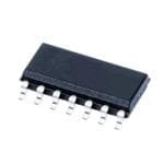
| 封装/外壳 | 14-SOIC(0.154",3.90mm 宽) |
| 封装/箱体 | SOIC-14 |
| 工作温度 | 0°C ~ 70°C |
| 工厂包装数量 | 50 |
| 开关频率 | 700 kHz |
| 拓扑结构 | Buck, Boost, Flyback, Forward |
| 最大工作温度 | + 70 C |
| 最小工作温度 | 0 C |
| 标准包装 | 50 |
| 电压-电源 | 10 V ~ 14 V |
| 类型 | Voltage Mode PWM Controllers |
| 系列 | UCC35701 |
| 输出数 | 1 |
| 输出电流 | 1000 mA |
| 输出端数量 | 1 Output |
| 降压 | 是 |
| 隔离式 | 是 |
| 频率-最大值 | 700kHz |


- 商务部:美国ITC正式对集成电路等产品启动337调查
- 曝三星4nm工艺存在良率问题 高通将骁龙8 Gen1或转产台积电
- 太阳诱电将投资9.5亿元在常州建新厂生产MLCC 预计2023年完工
- 英特尔发布欧洲新工厂建设计划 深化IDM 2.0 战略
- 台积电先进制程称霸业界 有大客户加持明年业绩稳了
- 达到5530亿美元!SIA预计今年全球半导体销售额将创下新高
- 英特尔拟将自动驾驶子公司Mobileye上市 估值或超500亿美元
- 三星加码芯片和SET,合并消费电子和移动部门,撤换高东真等 CEO
- 三星电子宣布重大人事变动 还合并消费电子和移动部门
- 海关总署:前11个月进口集成电路产品价值2.52万亿元 增长14.8%


PDF Datasheet 数据手册内容提取
application UCC15701/2 INFO UCC25701/2 available UCC35701/2 Advanced Voltage Mode Pulse Width Modulator FEATURES DESCRIPTION 700kHzOperation TheUCC35701/UCC35702familyofpulsewidthmodulatorsisintendedfor isolated switching power supplies using primary side control. They can be IntegratedOscillator/VoltageFeed used for both off-line applications and DC/DC converter designs such as in ForwardCompensation adistributedpowersystemarchitectureorasatelecompowersource. AccurateDutyCycleLimit The devices feature low startup current, allowing for efficient off-line start- AccurateVolt-secondClamp ing, yet have sufficient output drive to switch power MOSFETs in excess of 500kHz. OptocouplerInterface Voltage feed forward compensation is operational over a 5:1 input range FaultCountingShutdown and provides fast and accurate response to input voltage changes over a 4:1 range. An accurate volt-second clamp and maximum duty cycle limit FaultLatchofforAutomaticShutdown arealsofeatured. SoftStopOptimizedforSynchronous Faultprotectionisprovidedbypulsebypulsecurrentlimitingaswellasthe Rectification ability to latch off after a programmable number of repetitive faults has oc- 1APeakGateDriveOutput curred. 130(cid:1)AStart-upCurrent Two UVLO options are offered. UCC35701 family has turn-on and turn-off thresholdsof13V/9VandUCC35702familyhasthresholdsof9.6V/8.8V. 750(cid:1)AOperatingCurrent The UCC35701/2 and the UCC25701/2 are offered in the 14 pin SOIC (D), 14 pin PDIP (N) or in 14 pin TSSOP (PW) packages. The UCC15701/2 is offeredinthe14pinCDIP(J)package. TYPICAL APPLICATION DIAGRAM V SUPPLY IN R1 R6 R2 VFF R7 6 VDD 3 R3 7 RT VREF UCC35701 CT 10 CT C6VOUT R4 C1 C4 9 VSCLAMP R8 OUT 4 R5 11 SYNC CS R10 ILIM 2 14 SS C2 CF RCS 1 COUNT C3 RF 12 VREF PGND 5 R8 RGND VINRETURN 8 FB GND 13 R11 V OUT C5 R13 R12 C6 R14 C7 R15 UDG-98005-1 SLUS293C-JANUARY2000-REVISEDJUNE2005
UCC15701/2 UCC25701/2 UCC35701/2 ABSOLUTE MAXIMUM RATINGS ORDERING INFORMATION Supplyvoltage(Supplycurrentlimitedto20mA)........ 15V TA=TJ UVLO Package PartNumber SupplyCurrent................................. 20mA Option Inputpins(ILIM,VFF,RT,CT,VSCLAMP,SYNC,SS,FB)... 6V 13V/9V CDIP-14 UCC15701J –55°Cto+125°C OutputCurrent(OUT)DC..................... +/–180mA 9.6V/8.8V CDIP-14 UCC15702J OutputCurrent(OUT)Pulse(0.5ms).............. +/–1.2A SOIC-14 UCC25701D StorageTemperature................... –65°Cto+150°C 13V/9V PDIP-14 UCC25701N JunctionTemperature...................–55°Cto+150°C TSSOP-14 UCC25701PW LeadTemperature(Soldering,10sec.) ............ +300°C –40°Cto+85°C SOIC-14 UCC25702D Note: All voltages are with respect to GND. Currents are posi- 9.6V/8.8V PDIP-14 UCC25702N tive into the specified terminal. Consult Packaging Section of TSSOP-14 UCC25702PW the Databook for thermal limitations and considerations of SOIC-14 UCC35701D packages. 13V/9V PDIP-14 UCC35701N TSSOP-14 UCC35701PW 0°Cto+70°C CONNECTION DIAGRAMS SOIC-14 UCC35702D 9.6V/8.8V PDIP-14 UCC35702N DIL-14,SOIC-14,TSSOP-14(TOPVIEW) TSSOP-14 UCC35702PW Nor J,D, PWPACKAGE The D and PW packages are available taped and reeled. Add TRsuffixtothedevicetype(e.g.,UCC35701DTR). COUNT 1 14 SS ILIM 2 13 GND VDD 3 12 VREF OUT 4 11 SYNC PGND 5 10 CT VFF 6 9 VSCLAMP RT 7 8 FB ELECTRICAL CHARACTERISTICS:Unlessotherwisespecified,V =11V,RT=60.4k,C =330pF,C =C = DD T REF VDD 0.1(cid:1) F,V =2.0V,andnoloadontheoutputs. FF PARAMETER TESTCONDITIONS MIN TYP MAX UNITS UVLOSection StartThreshold (UCCX5701) 12 13 14 V (UCCX5702) 8.8 9.6 10.4 V StopThreshold (UCCX5701) 8 9 10 V (UCCX5702) 8.0 8.8 9.6 V Hysteresis (UCCX5701) 3 4 V (UCCX5702) 0.3 0.8 V SupplyCurrent Start-upCurrent (UCCX5701)V =11V,V ComparatorOff 130 200 (cid:1)A DD DD (UCCX5702)V =8V,V ComparatorOff 120 190 (cid:1)A DD DD IDDActive VDDComparatorOn 0.75 1.5 mA VDDClampVoltage (UCCX5701)IDD=10mA 13.5 14.3 15 V (UCCX5702)I =10mA 13 13.8 15 V DD VDDClamp–StartThreshold (UCCX5701) 1.3 V (UCCX5702) 4.2 V VoltageReference VREF VDD=10Vto13V,IVREF=0mAto2mA 4.9 5 5.1 V LineRegulation V =10Vto13V 20 mV DD LoadRegulation I =0mAto2mA 2 mV VREF ShortCircuitCurrent VREF=0V,TJ=25°C 20 50 mA 2
UCC15701/2 UCC25701/2 UCC35701/2 ELECTRICAL CHARACTERISTICS:Unlessotherwisespecified,V =11V,RT=60.4k,C =330pF,C =C = DD T REF VDD 0.1(cid:1) F,V =2.0V,andnoloadontheoutputs. FF PARAMETER TESTCONDITIONS MIN TYP MAX UNITS LineSense VthHighLineComparator 3.9 4 4.1 V VthLowLineComparator 0.5 0.6 0.7 V InputBiasCurrent –100 100 nA OscillatorSection Frequency V =0.8Vto3.2V 90 100 110 kHz FF Frequency V =0.6Vto3.4V(Note1) 90 100 110 kHz FF SYNCVIH 2 V SYNCVIL 0.8 V SYNCInputCurrent VSYNC=2.0V 3 10 (cid:1)A RTVoltage VFF=0.4V 0.5 0.6 0.7 V VFF=0.8V 0.75 0.8 0.85 V VFF=2.0V 1.95 2.0 2.05 V VFF=3.2V 3.15 3.2 3.25 V VFF=3.6V 3.3 3.4 3.5 V CTPeakVoltage VFF=0.8V(Note1) 0.8 V VFF=3.2V(Note1) 3.2 V CTValleyVoltage (Note1) 0 V SoftStart/Shutdown/DutyCycleControlSection ISSChargingCurrent 10 18 30 (cid:1)A ISSDischargingCurrent 300 500 750 (cid:1)A Saturation V =11V,ICOff 25 100 mV DD FaultCounterSection ThresholdVoltage VFF=0.8Vto3.2V 3.8 4 4.2 V SaturationVoltage VFF=0.8Vto3.2V 100 mV CountChargingCurrent 10 18 30 (cid:1)A CurrentLimitSection InputBiasCurrent –100 0 100 nA CurrentLimitThreshold 180 200 220 mV ShutdownThreshold 500 600 700 mV PulseWidthModulatorSection FBPinInputImpedance VFB=3V 30 50 100 k(cid:2) MinimumDutyCycle VFB<=1V 0 % MaximumDutyCycle VFB>=4.5V,VSCLAMP>=2.0V 95 99 100 % PWMGain VFF=0.8V 35 50 70 %/V VoltSecondClampSection MaximumDutyCycle VFF=0.8V,VSCLAMP=0.6V 69 74 79 % MinimumDutyCycle VFF=3.2V,VSCLAMP=0.6V 17 19 21 % OutputSection VOH I =–100mA,(V –V ) 0.4 1 V OUT DD OUT VOL I =100mA 0.4 1 V OUT RiseTime C =1000pF 20 100 ns LOAD FallTime C =1000pF 20 100 ns LOAD Note1:Ensuredbydesign.Not100%testedinproduction. 3
UCC15701/2 UCC25701/2 UCC35701/2 DETAILED BLOCK DIAGRAM 2*I RT S 11 SYNC VFF 6 3(cid:1) A Q R D RT 7 PEAK I RT 3 VDD CT 10 PWM 0.7V 0.2V VALLEY S Q 4 OUT + FB 8 R 1.5R R D 5 PGND VSCLAMP 9 4V HIGHLINE VREF RUN 13/9V(35701) LOWLINE 9.6/8.8V(35702) I 0.6V 4.5V SS 14 SSDONE 25*I 0.6V CURRENTFAULT R Q ILIM 2 CURRENTLIMIT 0.2V VDD 0.2V VREF SD D Q I FAULT PWM R Q LATCH 5.0V 12 VREF SSDONE R REF S D COUNT 1 4V 13 GND SHUTDOWN LATCH UDG-98004 PIN DESCRIPTIONS VDD: Power supply pin. A shunt regulator limits supply RT: The voltage on this pin mirrors VFF over a 0.8V to voltageto14Vtypicalat10mAshuntcurrent. 3.2V range. Aresistor to ground sets the ramp capacitor charge current. The resistor value should be between PGND: Power Ground. Ground return for output driver 20kand200k. andcurrents. CT: A capacitor to ground provides the oscillator/ GND:AnalogGround.Groundreturnforallothercircuits. feedforward sawtooth waveform. Charge current is 2 (cid:3) This pin must be connected directly to PGND on the I , resulting in a CT slope proportional to the input volt- board. RT age. TherampvoltagerangeisGNDtoV . RT OUT: Gate drive output. Output resistance is 10(cid:2) maxi- Periodandoscillatorfrequencyisgivenby: mum. V (cid:3)C VFF: Voltage feedforward pin. This pin connects to the T (cid:4) RT T (cid:5)tDISCH (cid:6)0.5(cid:3)RT (cid:3)CT 2(cid:3)I power supply input voltage through a resistive divider RT and provides feedforward compensation over a 0.8V to 2 F (cid:6) 3.2V range. A voltage greater than 4.0V or less than RT (cid:3)CT 0.6Vonthispininitiatesasoftstopcycle. 4
UCC15701/2 UCC25701/2 UCC35701/2 PIN DESCRIPTIONS (cont.) VSCLAMP: Voltage at this pin is compared to the CT source. While the soft start capacitor is charging, and voltage,providingaconstantvolt-secondlimit. Thecom- while VSS< (0.4 VFB), the duty cycle, and therefore the parator output terminates the PWM pulse when the ramp output voltage of the converter is determined by the soft voltage exceeds VSCLAMP. The maximum on time is startcircuitry. givenby: At High Line or Low Line fault conditions, the soft start V (cid:3)CT t (cid:4) VSCLAMP capacitor is discharged with a controlled discharge cur- ON 2(cid:3)IRT rent of about 500(cid:1)A. During the discharge time, the duty cycle of the converter is gradually decreased to zero. Themaximumdutycyclelimitisgivenby: This soft stop feature allows the synchronous rectifiers to t V D (cid:4) ON (cid:4) VSCLAMP gradually discharge the output LC filter. An abrupt shut MAX T V off can cause the LC filter to oscillate, producing unpre- RT dictableoutputvoltagelevels. FB:Input to the PWM comparator. This pin is intended tobedrivenwithanoptocouplercircuit. Inputimpedance All other fault conditions (UVLO, VREF Low, Over Cur- is50k(cid:2) Typicalmodulationrangeis1.6Vto3.6V. rent (0.6V on ILIM) or COUNT) will cause an immediate stopoftheconverter.Furthermore,boththeOverCurrent SYNC:Level sensitive oscillator sync input. Ahigh level fault and the COUNT fault will be internally latched until forces the gate drive output low and resets the ramp ca- V drops below 9V or V goes below the 600mV DD FF pacitor. On-time starts at the negative edge the pulse. thresholdattheinputoftheLowLinecomparator. There is a 3(cid:1)Apull down current on the pin, allowing it to After all fault conditions are cleared and the soft start ca- bedisconnectedwhennotused. pacitor is discharged below 200 mV, a soft start cycle will VREF: 5.0V trimmed reference with 2% variation over beinitiatedtorestarttheconverter. line, load and temperature. Bypass with a minimum of 0.1(cid:1)Ftoground. ILIM:Provides a pulse by pulse current limit by terminat- ing the PWM pulse when the input is above 200mV. An SS:Soft Start pin. Acapacitor is connected between this inputover600mVinitiatesalatchedsoftstopcycle. pin and ground to set the start up time of the converter. COUNT: Capacitor to ground integrates current pulses After power up (V >13V AND V >4.5V), or after a DD REF generated when ILIM exceeds 200mV. A resistor to fault condition has been cleared, the soft start capacitor is charged to V by a nominal 18(cid:1)A internal current ground sets the discharge time constant. A voltage over REF 4Vwillinitiatealatchedsoftstopcycle. APPLICATION INFORMATION (Note: Refer to the Typical Application Diagram on the first The circuit will start at this point. I will increase from VDD page of this datasheet for external component names.) All the the start up value of 130(cid:1)A to the run value of 750(cid:1)A. equations given below should be considered as first order ap- The capacitor on SS is charged with a 18(cid:1)A current. proximationswithfinalvaluesdeterminedempiricallyforaspe- When the voltage on SS is greater than 0.8V, output cificapplication. pulses can begin, and supply current will increase to a PowerSequencing level determined by the MOSFET gate charge require- VDD is normally connected through a high impedance ments to IVDD ~ 1mA + QT (cid:3) fs. When the output is ac- (R6) to the input line, with an additional path (R7) to a tive, the bootstrap winding should be sourcing the supply low voltage bootstrap winding on the power transformer. current. If VDD falls below the UVLO stop threshold, the VFF is connected through a divider (R1/R2) to the input controller will enter a shutdown sequence and turn the line. controller off, returning the start sequence to the initial condition. For circuit activation, all of the following conditions are required: VDDClamp An internal shunt regulator clamps VDD so the voltage 1. VFF between 0.6V and 4.0V (operational input voltage does not exceed a nominal value of 14V. If the regulator range). is active, supply current must be limited to less than 2.VDDhasbeenundertheUVLOstopthresholdtoreset 20mA. theshutdownlatch. 3.VDDisovertheUVLOstartthreshold. 5
UCC15701/2 UCC25701/2 UCC35701/2 APPLICATION INFORMATION (cont.) OutputInhibit VFF is intended to operate accurately over a 4:1 range between 0.8V and 3.2V. Voltages at VFF below 0.6V or During normal operation, OUT is driven high at the start above4.0Vwillinitiateasoftstopcycleandachiprestart of a clock period and is driven low by voltages on CT, FB whentheunder/overvoltageconditionisremoved. orVSCLAMP. Volt-SecondClamp The following conditions cause the output to be immedi- ately driven low until a clock period starts where none of Aconstantvolt-secondclampisformedbycomparingthe theconditionsaretrue: timing capacitor ramp voltage to a fixed voltage derived from the reference. Resistors R4 and R5 set the 1.I >0.2V LIM volt-second limit. For a volt-second product defined as 2.FBorSSislessthan0.8V VIN t ,therequiredvoltageatVSCLAMPis: ON(max) CurrentLimiting (cid:9) R2 (cid:12) (cid:7) (cid:8) (cid:11) (cid:14)(cid:3) V (cid:3)t ILIM is monitored by two internal comparators. The cur- (cid:10)R1(cid:5)R2(cid:13) IN ON(cid:7)max(cid:8) . rent limit comparator threshold is 0.2V. If the current limit R (cid:3)C T T comparator is triggered, OUT is immediately driven low and held low for the remainder of the clock cycle, provid- Thedutycyclelimitisthen: ing pulse-by-pulse over-current control for excessive V V VSCLAMP VSCLAMP ,or . loads. This comparator also causes CF to be charged for VVFF V (cid:3)(cid:9)(cid:11) R2 (cid:12)(cid:14) theremainderoftheclockcycle. IN (cid:10)R1(cid:5)R2(cid:13) If repetitive cycles are terminated by the current limit The maximum duty cycle is realized when the comparator causing COUNT to rise above 4V, the shut- feedforwardvoltageissetatthelowendoftheoperating down latch is set. The COUNT integration delay feature range(V =0.8V). will be bypassed by the shutdown comparator which has FF a 0.6V threshold. The shutdown comparator immediately Theabsolutemaximumdutycycleis: sets the shutdown latch. RF in parallel with CFresets the D (cid:4)VVSCLAMP (cid:4)VREF (cid:3) R5 COUNT integrator following transient faults. RF must be MAX 0.8 0.8 R4(cid:5)R5 greaterthan(4(cid:3)R4)(cid:3)(1–D ). MAX FrequencySet LatchedShutdown The frequency is set by a resistor from RTto ground and If ILIM rises above 0.6V, or COUNTrises to 4V, the shut- a capacitor from CTto ground. The frequency is approxi- down latch will be set. This will force OUTlow, discharge 2 SS and COUNT, and reduce I to approximately mately: F(cid:4) DD (R (cid:3)C ) 750(cid:1)A. When, and if, V falls below the UVLO stop T T DD threshold, the shutdown latch will reset and IDD will fall External synchronization is via the SYNC pin. The pin to 130(cid:1)A, allowing the circuit to restart. If VDD remains has a 1.5V threshold , making it compatible with 5V and above the UVLO stop threshold (within the UVLO band), 3.3VCMOSlogic.Theinputislevelsensitive,withahigh an alternate restart will occur if VFF is momentarily re- input forcing the oscillator ramp low and the output low. duced below 1V. External shutdown commands from any An active pull down on the SYNC pin allows it to be un- source may be added into either the COUNT or ILIM connectedwhennotused. pins. GateDriveOutput VoltageFeedforward The UCC35701/2 is capable of a 1Apeak output current. The voltage slope on CT is proportional to line voltage Bypass withatleast0.1(cid:1)FdirectlytoPGND.Thecapac- overa4:1rangeandequals2(cid:3)VFF(RT(cid:3)CT).Thecapac- itor must have a low equivalent series resistance and in- itor charging current is set by the voltage across RT. ductance. The connection from OUT to the power V(RT) tracks VFF over a range of 0.8V to 3.2V. Achang- MOSFET gate should have a 2(cid:2) or greater damping re- ing line voltage will immediately change the slope of sistor and the distance between chip and MOSFET V(CT),changingthepulsewidthinaproportionalmanner should be minimized. Alow impedance path must be es- without using the feedback loop, providing excellent dy- tablished between the MOSFET source (or ground side namiclineregulation. of the current sense resistor), the VDD capacitor and PGND.PGNDshouldthenbeconnectedbyasinglepath (shownasRGND)toGND. 6
UCC15701/2 UCC25701/2 UCC35701/2 APPLICATION INFORMATION (cont.) TransitioningFromUCC3570ToUCC35701 UCC35701/2 is pin to pin compatible to UCC3570 but is not a direct drop-in replacement for UCC3570 sockets. The UCC35701/2 is an advanced version of the popular, The changes required to the power supply printed circuit low power UCC3570 PWM. Significant improvements board of for existing UCC3570 designs are minimal. For were made to the IC’s oscillator and PWM control sec- conversion, only one extra resistor to set the volt-second tions to enhance overall system performance. All of the clamp needs to be added to the existing PC board lay- key attributes and functional blocks of the UCC3570 outs. In addition, some component values will need to were maintained in the UCC35701/2. A typical applica- be changed due to the functionality change in of four of tion using UCC3570 and UCC35701/2 is shown in Fig. 6 theICpins. forcomparison. ThePinoutChangesfromUCC3570areasfollows. The advantages of the UCC35701/2 over the UCC3570 areasfollows. Pin7waschangedfromSLOPEtoRT(fortiming resistor) Improved oscillatorandPWMcontrolsection. Pin8waschangedfromISETtoVSCLAMP(requiring Aprecisemaximumvolt-secondclampcircuit.The oneadditionalresistorfrompin9toVREF) UCC3570hasadualtimebasebetweenoscillatorand feedforwardcircuitry.Theintegatedtimebasein Pin10waschangedfromRAMPtoCT(singletiming UCC35701/2improvesthedutycycleclampaccuracy, capacitor) providingbetterthan (cid:15)5%accuratevolt-second clampoverfulltemperaturerange. Pin11waschangedfromFREQtoSYNC(inputonly) AdditionalInformation Separatelyprogrammableoscillatortimingresistor (RT)andcapacitor(CT)circuitsprovideahigher Please refer to the following two Unitrode application degreeofversatility. topicsonUCC3570foradditionalinformation. AnindependentSYNCinputpinforsimpleexternal [1] Application Note U-150, Applying the UCC3570 Volt- synchronization. age-Mode PWM Controller to Both Off-line and DC/DC ConverterDesignsbyRobertA.Mammano Asmallervaluefiltercapacitor(0.1(cid:1)F)canbeused withtheenhancedreferencevoltage. [2] Design Note DN-62, Switching Power Supply Topol- ogy, Voltage Mode vs. Current Mode by Robert Mammano TYPICAL WAVEFORMS FEEDBK VSCLAMP CT SOFTST SOFTSTART HIGHDC LOWDC ZERODC SOFTSTOP V-S CLAMP UDG-98207 Figure1.TimingdiagramforPWMactionwithforward,softstartandvolt-secondclamp. 7
UCC15701/2 UCC25701/2 UCC35701/2 TYPICAL WAVEFORMS (cont.) VFF CT SYNC UDG-98208 Figure2.Timingdiagramforoscillatorwaveformsshowingfeedforwardactionandsynchronization. TYPICAL CHARACTERISTIC CURVES 1000 1.03 VFF=3.2 E 1.02 L C z] Y H C 1.01 k Y Y[ UT VFF=0.8 C D N 100 100pF D 1.00 E E U 150pF Z EQ 220pF ALI 0.99 FR 330pF RM 470pF NO 0.98 10 0.97 20 60 100 140 180 220 -55 -35 -15 5 25 45 65 85 105 125 RT[K ] TEMPERATURE[°C] Figure3.Oscillatorfrequencyvs.RTandCT. Figure5.Normalizedmaximumdutycyclevs. temperature. 1.02 CT=330pF FOSC=100kHz Y C N 1.01 E U VFF=0.8 Q E R F D 1 E Z LI A M R 0.99 O N VFF=3.2 0.98 -55 -35 -15 5 25 45 65 85 105 125 TEMPERATURE[°C] Figure4.Oscillatorfrequencyvs.temperature. 8
UCC15701/2 UCC25701/2 UCC35701/2 APPLICATION INFORMATION (cont.) V IN+ R1 R5 R2 UCC3570 R6 6 VFF VDD 3 V OUT R3 C4 7 SLOPE C1 CR R8 10 RAMP OUT 4 R4 R9 9 ISET ILIM 2 C T C2 11 FREQ RT RSNS C SS 14 SS PGND 5 C F 1 COUNT R F R GND C3 12 VREF R7 GND 13 8 FB R11 V C5 OUT R13 R12 C6 R14 C7 R15 V IN+ R1 UCC35701 R5 R2 R6 6 VFF VDD 3 V OUT R3 C4 7 RT C1 CT R8 10 CT OUT 4 R4 R9 9 VSCLAMP ILIM 2 C2 R NEW 11 SYNC R SNS C SS 14 SS PGND 5 C F 1 COUNT R F R GND C3 12 VREF R7 GND 13 8 FB R11 V C5 OUT R13 R12 C6 R14 C7 R15 UDG-98210 Figure6.Single-endedforwardcircuitcomparisonbetweenUCC3570andUCC37501. 9
UCC15701/2 UCC25701/2 UCC35701/2 REVISION HISTORY DATE REVISION REASON 02/16/05 SLUS293B AddFBtoabsmaxtable.Createdrevisionhistorytable. 6/16/05 SLUS293C UpdatedblockdiagramandtheSSpindescription. 10
PACKAGE OPTION ADDENDUM www.ti.com 17-Oct-2018 PACKAGING INFORMATION Orderable Device Status Package Type Package Pins Package Eco Plan Lead/Ball Finish MSL Peak Temp Op Temp (°C) Device Marking Samples (1) Drawing Qty (2) (6) (3) (4/5) UCC25701D ACTIVE SOIC D 14 50 Green (RoHS CU NIPDAU Level-1-260C-UNLIM -40 to 85 UCC25701D & no Sb/Br) UCC25701DTR ACTIVE SOIC D 14 2500 Green (RoHS CU NIPDAU Level-1-260C-UNLIM -40 to 85 UCC25701D & no Sb/Br) UCC25701N ACTIVE PDIP N 14 25 Green (RoHS CU NIPDAU N / A for Pkg Type -40 to 85 UCC25701N & no Sb/Br) UCC25701NG4 ACTIVE PDIP N 14 25 Green (RoHS CU NIPDAU N / A for Pkg Type -40 to 85 UCC25701N & no Sb/Br) UCC25701PW ACTIVE TSSOP PW 14 90 Green (RoHS CU NIPDAU Level-2-260C-1 YEAR -40 to 85 25701 & no Sb/Br) UCC25701PWG4 ACTIVE TSSOP PW 14 90 Green (RoHS CU NIPDAU Level-2-260C-1 YEAR -40 to 85 25701 & no Sb/Br) UCC25702D ACTIVE SOIC D 14 50 Green (RoHS CU NIPDAU Level-1-260C-UNLIM -40 to 85 UCC25702D & no Sb/Br) UCC25702DTR ACTIVE SOIC D 14 2500 Green (RoHS CU NIPDAU Level-1-260C-UNLIM -40 to 85 UCC25702D & no Sb/Br) UCC25702N ACTIVE PDIP N 14 25 Green (RoHS CU NIPDAU N / A for Pkg Type -40 to 85 UCC25702N & no Sb/Br) UCC25702PW ACTIVE TSSOP PW 14 90 Green (RoHS CU NIPDAU Level-2-260C-1 YEAR -40 to 85 25702 & no Sb/Br) UCC25702PWG4 ACTIVE TSSOP PW 14 90 Green (RoHS CU NIPDAU Level-2-260C-1 YEAR -40 to 85 25702 & no Sb/Br) UCC25702PWTR ACTIVE TSSOP PW 14 2000 Green (RoHS CU NIPDAU Level-2-260C-1 YEAR -40 to 85 25702 & no Sb/Br) UCC25702PWTRG4 ACTIVE TSSOP PW 14 2000 Green (RoHS CU NIPDAU Level-2-260C-1 YEAR -40 to 85 25702 & no Sb/Br) UCC35701D ACTIVE SOIC D 14 50 Green (RoHS CU NIPDAU Level-1-260C-UNLIM 0 to 70 UCC35701D & no Sb/Br) UCC35701DTR ACTIVE SOIC D 14 2500 Green (RoHS CU NIPDAU Level-1-260C-UNLIM 0 to 70 UCC35701D & no Sb/Br) UCC35701N ACTIVE PDIP N 14 25 Green (RoHS CU NIPDAU N / A for Pkg Type 0 to 70 UCC35701N & no Sb/Br) UCC35701PW ACTIVE TSSOP PW 14 90 Green (RoHS CU NIPDAU Level-2-260C-1 YEAR 0 to 70 35701 & no Sb/Br) Addendum-Page 1
PACKAGE OPTION ADDENDUM www.ti.com 17-Oct-2018 Orderable Device Status Package Type Package Pins Package Eco Plan Lead/Ball Finish MSL Peak Temp Op Temp (°C) Device Marking Samples (1) Drawing Qty (2) (6) (3) (4/5) UCC35702D ACTIVE SOIC D 14 50 Green (RoHS CU NIPDAU Level-1-260C-UNLIM 0 to 70 UCC35702D & no Sb/Br) UCC35702N LIFEBUY PDIP N 14 25 Green (RoHS CU NIPDAU N / A for Pkg Type 0 to 70 UCC35702N & no Sb/Br) UCC35702PW ACTIVE TSSOP PW 14 90 Green (RoHS CU NIPDAU Level-2-260C-1 YEAR 0 to 70 35702 & no Sb/Br) (1) The marketing status values are defined as follows: ACTIVE: Product device recommended for new designs. LIFEBUY: TI has announced that the device will be discontinued, and a lifetime-buy period is in effect. NRND: Not recommended for new designs. Device is in production to support existing customers, but TI does not recommend using this part in a new design. PREVIEW: Device has been announced but is not in production. Samples may or may not be available. OBSOLETE: TI has discontinued the production of the device. (2) RoHS: TI defines "RoHS" to mean semiconductor products that are compliant with the current EU RoHS requirements for all 10 RoHS substances, including the requirement that RoHS substance do not exceed 0.1% by weight in homogeneous materials. Where designed to be soldered at high temperatures, "RoHS" products are suitable for use in specified lead-free processes. TI may reference these types of products as "Pb-Free". RoHS Exempt: TI defines "RoHS Exempt" to mean products that contain lead but are compliant with EU RoHS pursuant to a specific EU RoHS exemption. Green: TI defines "Green" to mean the content of Chlorine (Cl) and Bromine (Br) based flame retardants meet JS709B low halogen requirements of <=1000ppm threshold. Antimony trioxide based flame retardants must also meet the <=1000ppm threshold requirement. (3) MSL, Peak Temp. - The Moisture Sensitivity Level rating according to the JEDEC industry standard classifications, and peak solder temperature. (4) There may be additional marking, which relates to the logo, the lot trace code information, or the environmental category on the device. (5) Multiple Device Markings will be inside parentheses. Only one Device Marking contained in parentheses and separated by a "~" will appear on a device. If a line is indented then it is a continuation of the previous line and the two combined represent the entire Device Marking for that device. (6) Lead/Ball Finish - Orderable Devices may have multiple material finish options. Finish options are separated by a vertical ruled line. Lead/Ball Finish values may wrap to two lines if the finish value exceeds the maximum column width. Important Information and Disclaimer:The information provided on this page represents TI's knowledge and belief as of the date that it is provided. TI bases its knowledge and belief on information provided by third parties, and makes no representation or warranty as to the accuracy of such information. Efforts are underway to better integrate information from third parties. TI has taken and continues to take reasonable steps to provide representative and accurate information but may not have conducted destructive testing or chemical analysis on incoming materials and chemicals. TI and TI suppliers consider certain information to be proprietary, and thus CAS numbers and other limited information may not be available for release. In no event shall TI's liability arising out of such information exceed the total purchase price of the TI part(s) at issue in this document sold by TI to Customer on an annual basis. Addendum-Page 2
PACKAGE OPTION ADDENDUM www.ti.com 17-Oct-2018 Addendum-Page 3
PACKAGE MATERIALS INFORMATION www.ti.com 2-Sep-2015 TAPE AND REEL INFORMATION *Alldimensionsarenominal Device Package Package Pins SPQ Reel Reel A0 B0 K0 P1 W Pin1 Type Drawing Diameter Width (mm) (mm) (mm) (mm) (mm) Quadrant (mm) W1(mm) UCC25701DTR SOIC D 14 2500 330.0 16.4 6.5 9.0 2.1 8.0 16.0 Q1 UCC25702DTR SOIC D 14 2500 330.0 16.4 6.5 9.0 2.1 8.0 16.0 Q1 UCC25702PWTR TSSOP PW 14 2000 330.0 12.4 6.9 5.6 1.6 8.0 12.0 Q1 UCC35701DTR SOIC D 14 2500 330.0 16.4 6.5 9.0 2.1 8.0 16.0 Q1 PackMaterials-Page1
PACKAGE MATERIALS INFORMATION www.ti.com 2-Sep-2015 *Alldimensionsarenominal Device PackageType PackageDrawing Pins SPQ Length(mm) Width(mm) Height(mm) UCC25701DTR SOIC D 14 2500 333.2 345.9 28.6 UCC25702DTR SOIC D 14 2500 333.2 345.9 28.6 UCC25702PWTR TSSOP PW 14 2000 367.0 367.0 35.0 UCC35701DTR SOIC D 14 2500 333.2 345.9 28.6 PackMaterials-Page2
None
None
None
None
None
IMPORTANTNOTICEANDDISCLAIMER TIPROVIDESTECHNICALANDRELIABILITYDATA(INCLUDINGDATASHEETS),DESIGNRESOURCES(INCLUDINGREFERENCE DESIGNS),APPLICATIONOROTHERDESIGNADVICE,WEBTOOLS,SAFETYINFORMATION,ANDOTHERRESOURCES“ASIS” ANDWITHALLFAULTS,ANDDISCLAIMSALLWARRANTIES,EXPRESSANDIMPLIED,INCLUDINGWITHOUTLIMITATIONANY IMPLIEDWARRANTIESOFMERCHANTABILITY,FITNESSFORAPARTICULARPURPOSEORNON-INFRINGEMENTOFTHIRD PARTYINTELLECTUALPROPERTYRIGHTS. TheseresourcesareintendedforskilleddevelopersdesigningwithTIproducts.Youaresolelyresponsiblefor(1)selectingtheappropriate TIproductsforyourapplication,(2)designing,validatingandtestingyourapplication,and(3)ensuringyourapplicationmeetsapplicable standards,andanyothersafety,security,orotherrequirements.Theseresourcesaresubjecttochangewithoutnotice.TIgrantsyou permissiontousetheseresourcesonlyfordevelopmentofanapplicationthatusestheTIproductsdescribedintheresource.Other reproductionanddisplayoftheseresourcesisprohibited.NolicenseisgrantedtoanyotherTIintellectualpropertyrightortoanythird partyintellectualpropertyright.TIdisclaimsresponsibilityfor,andyouwillfullyindemnifyTIanditsrepresentativesagainst,anyclaims, damages,costs,losses,andliabilitiesarisingoutofyouruseoftheseresources. TI’sproductsareprovidedsubjecttoTI’sTermsofSale(www.ti.com/legal/termsofsale.html)orotherapplicabletermsavailableeitheron ti.comorprovidedinconjunctionwithsuchTIproducts.TI’sprovisionoftheseresourcesdoesnotexpandorotherwisealterTI’sapplicable warrantiesorwarrantydisclaimersforTIproducts. MailingAddress:TexasInstruments,PostOfficeBox655303,Dallas,Texas75265 Copyright©2019,TexasInstrumentsIncorporated