ICGOO在线商城 > 集成电路(IC) > PMIC - AC-DC 转换器,离线开关 > VIPER28HE
 Datasheet下载
- 型号: VIPER28HE
- 制造商: STMicroelectronics
- 库位|库存: xxxx|xxxx
- 要求:
| 数量阶梯 | 香港交货 | 国内含税 |
| +xxxx | $xxxx | ¥xxxx |
查看当月历史价格
查看今年历史价格
VIPER28HE产品简介:
ICGOO电子元器件商城为您提供VIPER28HE由STMicroelectronics设计生产,在icgoo商城现货销售,并且可以通过原厂、代理商等渠道进行代购。 VIPER28HE价格参考。STMicroelectronicsVIPER28HE封装/规格:PMIC - AC-DC 转换器,离线开关, Converter Offline Flyback Topology 115kHz 10-SDIP。您可以下载VIPER28HE参考资料、Datasheet数据手册功能说明书,资料中有VIPER28HE 详细功能的应用电路图电压和使用方法及教程。
STMicroelectronics的VIPER28HE是一款高性能、集成化PMIC(电源管理集成电路),主要用于AC-DC转换器和离线开关应用。它特别适用于需要高效、紧凑且可靠的电源解决方案的小功率设备中。以下是该型号的一些典型应用场景:

1. 消费类电子产品:
   - VIPER28HE广泛应用于各种家用电器,如智能插座、LED驱动器、智能家居设备等。这些设备通常需要一个稳定且高效的电源供应,以确保其正常运行。
   - 在便携式充电器和USB充电器中,VIPER28HE能够提供高效率的电源转换,减少热量生成并延长设备使用寿命。

2. 工业控制与自动化:
   - 用于工业传感器、PLC(可编程逻辑控制器)和其他低功耗工业设备。这类设备通常需要在较宽的输入电压范围内工作,并且要求具备较高的可靠性和稳定性。
   - VIPER28HE可以为这些设备提供稳定的直流输出,同时保持较低的待机功耗,有助于提高系统的整体能效。

3. 医疗设备:
   - 在小型医疗仪器和便携式健康监测设备中,VIPER28HE提供了安全可靠的电源管理功能。例如,血压计、血糖仪等设备需要精确稳定的电源来保证测量结果的准确性。
   - 它还支持多种保护机制,如过压保护、短路保护等,从而增强了设备的安全性。

4. 通信设备:
   - 适用于路由器、调制解调器以及其他网络终端设备。这些设备通常需要一个稳定的电源供应,以确保数据传输的连续性和可靠性。
   - VIPER28HE能够在较宽的工作温度范围内提供稳定的性能,适应不同的环境条件。

总之,VIPER28HE凭借其高效的转换效率、紧凑的设计以及丰富的保护功能,在众多小功率应用领域展现了卓越的表现。
| 参数 | 数值 |
| 产品目录 | 集成电路 (IC)半导体 |
| 描述 | IC OFFLINE CONV PWM 800V 10-SDIP交流/直流转换器 VIPer28 Rugged 800V Fixed freq 115 kHz |
| 产品分类 | |
| 品牌 | STMicroelectronics |
| 产品手册 | |
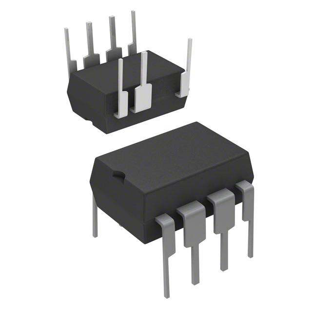
| 产品图片 |
|
| rohs | 符合RoHS无铅 / 符合限制有害物质指令(RoHS)规范要求 |
| 产品系列 | 电源管理 IC,交流/直流转换器,STMicroelectronics VIPER28HEVIPer™ plus |
| 数据手册 | |
| 产品型号 | VIPER28HE |
| 产品培训模块 | http://www.digikey.cn/PTM/IndividualPTM.page?site=cn&lang=zhs&ptm=30015 |
| 产品种类 | 交流/直流转换器 |
| 供应商器件封装 | 10-SDIP |
| 其它名称 | 497-10746-5 |
| 其它有关文件 | http://www.st.com/web/catalog/sense_power/FM142/CL1454/SC432/SS1635/PF216899?referrer=70071840 |
| 功率(W) | 20W |
| 包装 | 管件 |
| 占空比-最大 | 80 % |
| 商标 | STMicroelectronics |
| 安装风格 | Through Hole |
| 封装 | Tube |
| 封装/外壳 | 10-SDIP (0.300", 7.62mm) |
| 封装/箱体 | SDIP-10 |
| 工作温度 | -25°C ~ 125°C |
| 工作温度范围 | - 25 C to + 125 C |
| 工厂包装数量 | 50 |
| 开关频率 | 115 kHz |
| 拓扑结构 | Flyback |
| 标准包装 | 50 |
| 特色产品 | http://www.digikey.com/cn/zh/ph/ST/VIPerPlus.htmlhttp://www.digikey.cn/product-highlights/cn/zh/stmicroelectronics-viperplus-converters/3895 |
| 电压-击穿 | 800V |
| 电压-输入 | 8.5 V ~ 23.5 V |
| 电压-输出 | - |
| 电源电流 | 2.5 mA |
| 相关产品 | /product-detail/zh/750871110/732-2258-ND/2208834 |
| 类型 | Off Line High Voltage Converter |
| 系列 | VIPER28 |
| 绝缘 | Isolated |
| 输入/电源电压—最大值 | 23.5 V |
| 输入/电源电压—最小值 | 8.5 V |
| 输出功率 | 20 W |
| 输出电压 | 800 V |
| 输出电流 | 1.2 A |
| 输出端数量 | 1 Output |
| 输出隔离 | 隔离 |
| 配用 | /product-detail/zh/STEVAL-ISA126V1/497-14483-ND/4759355 |
| 频率范围 | 103kHz ~ 127kHz |


- 商务部:美国ITC正式对集成电路等产品启动337调查
- 曝三星4nm工艺存在良率问题 高通将骁龙8 Gen1或转产台积电
- 太阳诱电将投资9.5亿元在常州建新厂生产MLCC 预计2023年完工
- 英特尔发布欧洲新工厂建设计划 深化IDM 2.0 战略
- 台积电先进制程称霸业界 有大客户加持明年业绩稳了
- 达到5530亿美元!SIA预计今年全球半导体销售额将创下新高
- 英特尔拟将自动驾驶子公司Mobileye上市 估值或超500亿美元
- 三星加码芯片和SET,合并消费电子和移动部门,撤换高东真等 CEO
- 三星电子宣布重大人事变动 还合并消费电子和移动部门
- 海关总署:前11个月进口集成电路产品价值2.52万亿元 增长14.8%


PDF Datasheet 数据手册内容提取
VIPER28 Off-line high voltage converters − Datasheet production data Features ■ 800 V avalanche rugged power section ■ PWM operation with adjustable limiting current ■ 30 mW stand-by power at 265 Vac ■ Operating frequency: SDIP10 SO16 narrow DIP-7 SO 16 – 60 kHz for L type Description – 115 kHz for H type ■ Frequency jittering for low EMC The device is an off-line converter with an 800 V rugged power section, a PWM control, two levels ■ Output overvoltage protection of over-current protection, over-voltage and ■ High primary current protection (2nd OCP) overload protections, hysteretic thermal ■ Extra power timer for peak current protection, soft-start and safe auto-restart after management any fault condition removal. Burst mode operation and device very low consumption help to meet the ■ On-board soft-start standby energy saving regulations. Advance ■ Safe auto-restart after a fault condition frequency jittering reduces EMI filter cost. The ■ Hysteretic thermal shutdown extra power timer allows the management of output peak power for a designed time window. Application The high voltage start-up circuit is embedded in the device. ■ Auxiliary power supply for consumer and home Figure 1. Typical application equipment ■ ATX auxiliary power supply + + DC input high voltage ■ Low / medium power AC-DC adapters w-ide range DC Output voltage - ■ SMPS for set-top boxes, DVD players and recorders, white goods DRAIN DRAIN EPT VIPER28 GND VDD CONT FB Table 1. Device summary Order codes Package Packaging VIPER28LN / VIPER28HN DIP-7 VIPER28LE / VIPER28HE SDIP10 Tube VIPER28HD / VIPER28LD SO16 narrow VIPER28HDTR / VIPER28LDTR Tape and reel January 2013 Doc ID 15028 Rev 5 1/32 This is information on a product in full production. www.st.com 32
Contents VIPER28 Contents 1 Block diagram . . . . . . . . . . . . . . . . . . . . . . . . . . . . . . . . . . . . . . . . . . . . . . 3 2 Typical power . . . . . . . . . . . . . . . . . . . . . . . . . . . . . . . . . . . . . . . . . . . . . . . 3 3 Pin settings . . . . . . . . . . . . . . . . . . . . . . . . . . . . . . . . . . . . . . . . . . . . . . . . 4 4 Electrical data . . . . . . . . . . . . . . . . . . . . . . . . . . . . . . . . . . . . . . . . . . . . . . 5 4.1 Maximum ratings . . . . . . . . . . . . . . . . . . . . . . . . . . . . . . . . . . . . . . . . . . . . 5 4.2 Thermal data . . . . . . . . . . . . . . . . . . . . . . . . . . . . . . . . . . . . . . . . . . . . . . . 5 4.3 Electrical characteristics . . . . . . . . . . . . . . . . . . . . . . . . . . . . . . . . . . . . . . . 6 5 Typical electrical characteristics . . . . . . . . . . . . . . . . . . . . . . . . . . . . . . 10 6 Typical circuit . . . . . . . . . . . . . . . . . . . . . . . . . . . . . . . . . . . . . . . . . . . . . 13 7 Operation descriptions . . . . . . . . . . . . . . . . . . . . . . . . . . . . . . . . . . . . . . 14 7.1 Power section and gate driver . . . . . . . . . . . . . . . . . . . . . . . . . . . . . . . . . 14 7.2 High voltage startup generator . . . . . . . . . . . . . . . . . . . . . . . . . . . . . . . . . 14 7.3 Power-up and soft-start up . . . . . . . . . . . . . . . . . . . . . . . . . . . . . . . . . . . . 15 7.4 Power down operation . . . . . . . . . . . . . . . . . . . . . . . . . . . . . . . . . . . . . . . 17 7.5 Auto restart operation . . . . . . . . . . . . . . . . . . . . . . . . . . . . . . . . . . . . . . . . 17 7.6 Oscillator . . . . . . . . . . . . . . . . . . . . . . . . . . . . . . . . . . . . . . . . . . . . . . . . . 17 7.7 Current mode conversion with adjustable current limit set point . . . . . . . 18 7.8 Overvoltage protection (OVP) . . . . . . . . . . . . . . . . . . . . . . . . . . . . . . . . . 18 7.9 About CONT pin . . . . . . . . . . . . . . . . . . . . . . . . . . . . . . . . . . . . . . . . . . . . 20 7.10 Feed-back and overload protection (OLP) . . . . . . . . . . . . . . . . . . . . . . . . 20 7.11 Burst-mode operation at no load or very light load . . . . . . . . . . . . . . . . . . 23 7.12 Extra power management function (EPT) . . . . . . . . . . . . . . . . . . . . . . . . 24 7.13 2nd level overcurrent protection and hiccup mode . . . . . . . . . . . . . . . . . . 25 8 Package mechanical data . . . . . . . . . . . . . . . . . . . . . . . . . . . . . . . . . . . . 26 9 Revision history . . . . . . . . . . . . . . . . . . . . . . . . . . . . . . . . . . . . . . . . . . . 31 2/32 Doc ID 15028 Rev 5
VIPER28 Block diagram 1 Block diagram Figure 2. Block diagram VDD DDRRAAIINN LLEEBB EPTTToovvll ETTPooTvvll RRIInneetteeffeerrnnrreeaannll ccSS&&eeuu ppVVppoollyyllttaa bbgguueessss SS&&UU UUPPVVPPLLLLOOYY HHVV__OONN IDDch BBLLOOCCKK OOSSCCIILLLLAATTOORR UUVVLLOO TTHHEERRMMAALL SSHHUUTTDDOOWWNN OOLLPP OOTTPP TTUURRNN--OONN CCOONNTT SSSSTTOOAAFRFRTTTT BBOOLLCCOOPPCCKK -- OOCCPP BBUURRSSTT LLOOGGIICC SS QQ ++ LLEEBB RR OOVVPP DDLLOOEEGGTTEEIICCCCTTIIOONN ++ PPWWMM QQ SS HHVV__OONN BBPLPLOOWWCCMMKK -- 22nndd OOCCPP-- 22nndd OOCCPP RR ++ ++ LLOOGGIICC OOVVPP -- DDiissaabbllee OOTTPP OOVVPP OOLLPP RRsseennssee BBUURRSSTT--MMOODDEE BBUURRSSTT LLOOGGIICC FFBB GGNNDD 2 Typical power Table 2. T ypical power 230 V 85-265 V AC AC Part number Adapter(1) Open frame(2) Adapter(1) Open frame(2) VIPER28 18 W 20 W 10 W 12 W 1. Typical continuous power in non ventilated enclosed adapter measured at 50 °C ambient. 2. Maximum practical continuous power in an open frame design at 50 °C ambient, with adequate heat sinking. Doc ID 15028 Rev 5 3/32
Pin settings VIPER28 3 Pin settings Figure 3. Connection diagram (top view) Note: The copper area for heat dissipation has to be designed under the DRAIN pins. Table 3. Pin description Pin n. Name Function SDIP10 DIP-7 SO16N 1 1 1...2 GND This pin represents the device ground and the source of the power section. Function: Not available for user. It can be connected to GND (pins 1-2) or left - - 4 N.A. not connected. Supply voltage of the control section. This pin also provides the charging 2 2 5 VDD current of the external capacitor during start-up time. Control pin. The following functions can be selected: 1. current limit set point adjustment. The internal set default value of the cycle- by-cycle current limit can be reduced by connecting to ground an external 3 3 6 CONT resistor. 2. output voltage monitoring. A voltage exceeding V threshold (see Table8 OVP on page7) shuts the IC down reducing the device consumption. This function is strobed and digitally filtered for high noise immunity. Control input for duty cycle control. Internal current generator provides bias current for loop regulation. A voltage below the threshold V activates the 4 4 7 FB FBbm burst-mode operation. A level close to the threshold V means that we are FBlin approaching the cycle-by-cycle over-current set point. This pin allows the connection of an external capacitor for the extra power 5 5 8 EPT management. If the function is not used, the pin has to be connected to GND. High voltage drain pin. The built-in high voltage switched start-up bias current 6...10 7,8 13...16 DRAIN is drawn from this pin too. Pins connected to the metal frame to facilitate heat dissipation. 4/32 Doc ID 15028 Rev 5
VIPER28 Electrical data 4 Electrical data 4.1 Maximum ratings Table 4. Absolute maximum ratings Value Symbol Parameter Unit Min Max V Drain-to-source (ground) voltage 800 V DRAIN E Repetitive avalanche energy (limited by T = 150 °C) 3.5 mJ AV J I Repetitive avalanche current (limited by T = 150 °C) 1 A AR J I Pulse drain current (limited by T = 150°C) 3 A DRAIN J V Control input pin voltage -0.3 6 V CONT V Feed-back voltage -0.3 5.5 V FB V EPT input pin voltage -0.3 5 V EPT V Supply voltage (I = 25 mA) -0.3 Self limited V DD DD I Input current 25 mA DD Power dissipation at T < 40 °C (DIP-7) 1 A P W TOT Power dissipation at T < 60 °C (SO16N, SDIP-10) 1.5 A T Operating junction temperature range -40 150 °C J T Storage temperature -55 150 °C STG 4.2 Thermal data Table 5. Thermal data Max value Symbol Parameter Unit SO16N DIP7 SDIP10 Thermal resistance junction pin R 25 35 35 °C/W thJP (Dissipated power = 1 W) Thermal resistance junction ambient R 60 100 80 °C/W thJA (Dissipated power = 1 W) Thermal resistance junction ambient (1) R 50 80 65 °C/W thJA (Dissipated power = 1 W) 1. When mounted on a standard single side FR4 board with 100 mm2 (0.155 sq in) of Cu (35 µm thick) Doc ID 15028 Rev 5 5/32
Electrical data VIPER28 4.3 Electrical characteristics (T = -25 to 125 °C, V = 14 V (a); unless otherwise specified) J DD Table 6. P ower section Symbol Parameter Test condition Min Typ Max Unit V Break-down voltage I = 1 mA, V = GND, T = 25 °C 800 V BVDSS DRAIN FB J I OFF state drain current V = max rating,V = GND, T = 25°C 60 μA OFF DRAIN FB J Drain-source on state IDRAIN = 0.4 A, VFB = 3 V, VEPT = GND, TJ = 25 °C 7 Ω R DS(on) resistance I = 0.4 A, V = 3 V, V = GND, T = 125 °C 14 Ω DRAIN FB EPT J Effective (energy related) C V = 0 to 640 V, T = 25°C 40 pF OSS output capacitance DRAIN J Table 7. S upply section Symbol Parameter Test condition Min Typ Max Unit Voltage V Drain-source start voltage 60 80 100 V DRAIN_START V = 120 V, V = GND, DRAIN EPT -2 -3 -4 mA V = GND, V = 4 V FB DD I Start up charging current DDch V = 120 V, V = GND, DRAIN EPT -0.4 -0.6 -0.8 mA V = GND, V = 4 V after fault FB DD V Operating voltage range After turn-on 8.5 23.5 V DD V V clamp voltage I = 20 mA 23.5 V DDclamp DD DD V V start up threshold 13 14 15 V DDon DD V = 120 V, V = GND, DRAIN EPT VDDoff VthDreDs uhnodlder voltage shutdown VFB = GND 7.5 8 8.5 V V = 120 V, V = GND, VDD(RESTART) VDD restart voltage threshold VDR =A IGNND EPT 4 4.5 5 V FB Current I Operating supply current, not VFB = GND, FSW = 0 kHz 0.9 mA DD0 switching V = GND, V = 10 V EPT DD Operating supply current, VDRAIN = 120 V, FSW = 60 kHz 2.5 mA I DD1 switching V = 120 V,F = 115 kHz 3.5 mA DRAIN SW Operating supply current, with I V = 10 V 400 uA DD_FAULT protection tripping DD Operating supply current with I V = 7 V 270 uA DD_OFF V < V DD DD DD_OFF a. Adjust V above V start-up threshold before setting to 14 V DD DDon 6/32 Doc ID 15028 Rev 5
VIPER28 Electrical data Table 8. C ontroller section Symbol Parameter Test condition Min Typ Max Unit Feed-back pin V Over-load shut down threshold 4.5 4.8 5.2 V FBolp V Linear dynamics upper limit 3.2 3.5 3.7 V FBlin V Burst mode threshold Voltage falling 0.6 V FBbm V Burst mode hysteresis Voltage rising 100 mV FBbmhys V = 0.3 V -150 -200 -280 uA FB I Feed-back sourced current FB 3.3 V < V < 4.8 V -3 uA FB R Dynamic resistance V < 3.3 V 14 20 kΩ FB(DYN) FB H ΔV / ΔI 2 6 V/A FB FB D CONT pin V Low level clamp voltage I = -100 µA 0.5 V CONT_l CONT V High level clamp voltage I = 1mA 5 5.5 6 V CONT_h CONT Current limitation V = 4 V, I = -10 µA I Max drain current limitation FB CONT 0.75 0.80 0.85 A Dlim T = 25 °C J t Soft-start time 8.5 ms SS T Minimum turn ON time 220 400 480 ns ON_MIN td Propagation delay 100 ns t Leading edge blanking 300 ns LEB I Peak drain current during burst mode V = 0.6 V 160 mA D_BM FB Oscillator section VIPER28L V = operating voltage 54 60 66 kHz F DD OSC VIPER28H range, VFB = 1 V 103 115 127 kHz VIPER28L ±4 kHz FD Modulation depth VIPER28H ±8 kHz FM Modulation frequency 250 Hz D Maximum duty cycle 70 80 % MAX Doc ID 15028 Rev 5 7/32
Electrical data VIPER28 Table 8. C ontroller section (continued) Symbol Parameter Test condition Min Typ Max Unit Over-current protection (2nd OCP) I Second over-current threshold 1.2 A DMAX Over-voltage protection V Over-voltage protection threshold 2.7 3 3.3 V OVP T Over-voltage protection strobe time 2.2 us STROBE Extra power management I Drain current limit with EPT function ICONT < -10 μA 85% A DLIM_EPT T = 25 °C IDlim J V EPT shut down threshold 4 V EPT(STOP) VEPT(RESTART) EPT restart threshold ICONT < -10 μA 0.6 V I Sourced EPT current 5 μA EPT Thermal shutdown T Thermal shutdown temperature 150 160 °C SD T Thermal shutdown hysteresis 30 °C HYST 8/32 Doc ID 15028 Rev 5
VIPER28 Electrical data Figure 4. Minimum turn-on time test circuit VDRAIN GND DRAIN 90 % VDD DRAIN TONmin 14 V CONT 50 Ω 10 % IDRAIN Time FB EPT 3.5 V 30 V IDLIM Time Figure 5. OVP threshold test circuits VCONT GND DRAIN VOVP VDD DRAIN 14 V CONT 10 kΩ VDRAIN Time FB EPT 30 V 2 V Time Note: Adjust V above V start-up threshold before setting to 14 V DD DDon Doc ID 15028 Rev 5 9/32
Typical electrical characteristics VIPER28 5 Typical electrical characteristics Figure 6. C urrent limit vs T Figure 7. Switching frequency vs T J J Figure 8. Drain start-up voltage vs T Figure 9. HFB vs T J J Figure 10. O perating supply current Figure 11. Operating supply current (no switching) vs T (switching) vs T J J 10/32 Doc ID 15028 Rev 5
VIPER28 Typical electrical characteristics Figure 12. Current limit vs R Figure 13. Power MOSFET on-resistance vs T LIM J Figure 14. Power MOSFET break down voltage vs T J Doc ID 15028 Rev 5 11/32
Typical electrical characteristics VIPER28 Figure 15. Thermal shutdown V DD V DDon V DDoff V DD(RESTART) I time DRAIN time T J T SD T -T SD HYST time Normal operation Shut down after over temperature Normal operation 12/32 Doc ID 15028 Rev 5
VIPER28 Typical circuit 6 Typical circuit Figure 16. Min-features flyback application EPT Figure 17. Full-feature flyback application EPT Doc ID 15028 Rev 5 13/32
Operation descriptions VIPER28 7 Operation descriptions The device is a high-performance low-voltage PWM controller chip with an 800 V, avalanche rugged Power section. The controller includes: the oscillator with jittering feature, the start up circuits with soft-start feature, the PWM logic, the current limit circuit with adjustable set point, the second overcurrent circuit, the burst mode management, the brown-out circuit, the UVLO circuit, the auto-restart circuit and the thermal protection circuit. The current limit set-point is set by the CONT pin. The burst mode operation guaranties high performance in the stand-by mode and helps in the energy saving norm accomplishment. All the fault protections are built in auto restart mode with very low repetition rate to prevent IC's over heating. 7.1 Power section and gate driver The power section is implemented with an avalanche ruggedness N-channel MOSFET, which guarantees safe operation within the specified energy rating as well as high dv/dt capability. The power section has a B of 800 V min. and a typical R of 7 Ω VDSS DS(on) at 25 °C. The integrated SenseFET structure allows a virtually loss-less current sensing. The gate driver is designed to supply a controlled gate current during both turn-on and turn- off in order to minimize common mode EMI. Under UVLO conditions an internal pull-down circuit holds the gate low in order to ensure that the power section cannot be turned on accidentally. 7.2 High voltage startup generator The HV current generator is supplied through the DRAIN pin and it is enabled only if the input bulk capacitor voltage is higher than V threshold, 80 V typically. When DRAIN_START DC the HV current generator is ON, the I current (3 mA typical value) is delivered to the DDch capacitor on the V pin. In case of auto restart mode after a fault event, the I current is DD DDch reduced to 0.6 mA, in order to have a slow duty cycle during the restart phase. 14/32 Doc ID 15028 Rev 5
VIPER28 Operation descriptions 7.3 Power-up and soft-start up If the input voltage rises up till the device start threshold, V , the V voltage DRAIN_START DD begins to grow due to the I current (see Table7 on page6) coming from the internal DDch high voltage start up circuit. If the V voltage reaches V threshold (see Table7 on DD DDon page6) the power MOSFET starts switching and the HV current generator is turned OFF. See Figure18 on page15. The IC is powered by the energy stored in the capacitor on the VDD pin, C , until when VDD the self-supply circuit (typically an auxiliary winding of the transformer and a steering diode) develops a voltage high enough to sustain the operation. C capacitor must be sized enough to avoid fast discharge and keep the needed voltage VDD value higher than V threshold. In fact, a too low capacitance value could terminate the DDoff switching operation before the controller receives any energy from the auxiliary winding. The following formula can be used for the V capacitor calculation: DD Equation 1 I × t C = ---D----D----c---h-----------S----S---a---u---x-- VDD V –V DDon DDoff The t is the time needed for the steady state of the auxiliary voltage. This time is SSaux estimated by applicator according to the output stage configurations (transformer, output capacitances, etc.). During the converter start up time, the drain current limitation is progressively increased to the maximum value. In this way the stress on the secondary diode is considerably reduced. It also helps to prevent transformer saturation. The soft-start time lasts 8.5 ms and the feature is implemented for every attempt of start up converter or after a fault. Figure 18. I current during start-up and burst mode DD V DD V DDon V DDoff V t FB V FBolp V FBlin V V FBbmhys FBbm t V DRAIN I t DD I DD1 I DD0 t I (-3 mA) DDch START-UP NORMAL MODE BURST MODE NORMAL MODE Doc ID 15028 Rev 5 15/32
Operation descriptions VIPER28 Figure 19. Timing diagram: normal power-up and power-down sequences V IN VIN< VDRAIN_START HV startup is no more activated V DRAIN_START VDD regulation is lost here time V DDon V DDoff V DD(RESTART) VDRAIN time I DD time I (3mA) DDch time Power-on Normal operation Power-off Figure 20. Soft-start: timing diagram IDRAIN tSS(soft start) IDlim t VFB TOLP-delay VFBolp VFBlin VOUT t Regulated value t 16/32 Doc ID 15028 Rev 5
VIPER28 Operation descriptions 7.4 Power down operation At converter power down, the system loses regulation as soon as the input voltage is so low that the peak current limitation is reached. The V voltage drops and when it falls below DD the V threshold (see Table7 on page6) the power MOSFET is switched OFF, the DDoff energy transfers to the IC interrupted and consequently the V voltages decreases, DD Figure19 on page16. Later, if the V is lower than V (see Table7 on page6), IN DRAIN_START the start up sequence is inhibited and the power down completed. This feature is useful to prevent converter’s restart attempts and ensures monotonic output voltage decay during the system power down. 7.5 Auto restart operation If after a converter power down, the V is higher than V the start up sequence IN DRAIN_START, is not inhibited and will be activated only when the V voltage drops down the DD V threshold (see Table7 on page6). This means that the HV start up current DD(RESTART) generator restarts the V capacitor charging only when the V voltage drops below DD DD V . The scenario above described is for instance a power down because of a DD(RESTART) fault condition. After a fault condition, the charging current, I , is 0.6 mA (typ.) instead of DDch the 3 mA (typ.) of a normal start up converter phase. This feature together with the low V threshold ensures that, after a fault, the restart attempts of the IC has a very DD(RESTART) long repetition rate and the converter works safely with extremely low power throughput. The Figure21 shows the IC behavioral after a short-circuit event. Figure 21. Timing diagram: behavior after short-circuit V Short circuit occurs here DD VDDon VDDoff VDD(RESTART) V FB time VFBolp VFBlin VDS TREPETITION time = 0.3 x TREPETITION I DD time IDDch (0.6mA) time 7.6 Oscillator The switching frequency is internally fixed to 60 kHz or 115 kHz. In both case the switching frequency is modulated by approximately ±4 kHz (60 kHz version) or ±8 kHz (115 kHz version) at 250 Hz (typical) rate, so that the resulting spread-spectrum action distributes the energy of each harmonic of the switching frequency over a number of side- band harmonics having the same energy on the whole but smaller amplitudes. Doc ID 15028 Rev 5 17/32
Operation descriptions VIPER28 7.7 Current mode conversion with adjustable current limit set point The device is a current mode converter: the drain current is sensed and converted in voltage that is applied to the non inverting pin of the PWM comparator. This voltage is compared with the one on the feed-back pin through a voltage divider on cycle by cycle basis. The device has a default current limit value, I , that the designer can adjust according the Dlim electrical specification, by the R resistor connected to the CONT, see Figure12 on LIM page11. The CONT pin has a minimum current sunk needed to activate the I adjustment: without Dlim R or with high R (i.e. 100 kΩ) the current limit is fixed to the default value (see I , LIM LIM Dlim Table8 on page7). 7.8 Overvoltage protection (OVP) The device has integrated the logic for the monitor of the output voltage using as input signal the voltage V during the OFF time of the power MOSFET. This is the time when the CONT voltage from the auxiliary winding tracks the output voltage, through the turn ratio N-----A----U---X-- N SEC The CONT pin has to be connected to the auxiliary winding through the diode D and the OVP resistors R and R as shows the Figure23 on page20 When, during the OFF time, OVP LIM the voltage V exceeds, four consecutive times, the reference voltage V (see Table8 CONT OVP on page7) the overvoltage protection will stop the power MOSFET and the converter enters the auto-restart mode. In order to bypass the noise immediately after the turn off of the power MOSFET, the voltage V is sampled inside a short window after the time T , see Table8 on page7 and CONT STROBE the Figure22 on page19. The sampled signal, if higher than V , trigger the internal OVP OVP digital signal and increments the internal counter. The same counter is reset every time the signal OVP is not triggered in one oscillator cycle. Referring to the Figure23, the resistors divider ratio k will be given by: OVP Equation 2 V k = ------------------------------------------------O----V----P--------------------------------------------- OVP N -----A----U---X--⋅ (V +V )–V N OUTOVP DSEC DAUX SEC Equation 3 R k = ----------------L---I-M-------------- OVP R +R LIM OVP 18/32 Doc ID 15028 Rev 5
VIPER28 Operation descriptions Where: ● V is the OVP threshold (see Table8 on page8) OVP ● V is the converter output voltage value to activate the OVP set by designer OUT OVP ● N is the auxiliary winding turns AUX ● N is the secondary winding turns SEC ● V is the secondary diode forward voltage DSEC ● V is the auxiliary diode forward voltage DAUX ● R together R make the output voltage divider OVP LIM Than, fixed R according to the desired I , the R can be calculating by: LIM, Dlim OVP Equation 4 1–k R = R × -------------O----V---P--- OVP LIM k OVP The resistor values will be such that the current sourced and sunk by the CONT pin be within the rated capability of the internal clamp. Figure 22. OVP timing diagram VVDDSS t VAUX 00 VCONT tt VOVP tt SSTTRROOBBEE TSTROBE Sampling time tt OOVVPP tt CCOOUUNNTTEERR RREESSEETT CCOOUUNNTTEERR tt SSTTAATTUUSS 00 00 00 00 →→11 11 →→22 22 →→00 00 00 →→11 11 →→ 22 22 →→33 33 →→ 44 FFAAUULLTT tt tt NNOORRMMAALL OOPPEERRAATTIIOONN TTEEMMPPOORRAARRYY DDIISSTTUURRBBAANNCCEE FFEEEEDDBBAACCKK LLOOOOPP FFAAIILLUURREE Doc ID 15028 Rev 5 19/32
Operation descriptions VIPER28 7.9 About CONT pin Referring to the Figure23, through the CONT pin, the below features can be implemented: 1. Current limit set point 2. Overvoltage protection on the converter output voltage The Table9 on page20 referring to the Figure23, lists the external components needed to activate one or plus of the CONT pin functions. Figure 23. CONT pin configuration SOFT Daux ROVP CONT START OCP - OCP BLOCK + to GATE driver Auxiliary winding RLIM OVP LOGIC From RSENSE OVP Table 9. CONT pin configurations Function / component R (1) R D LIM OVP AUX I reduction See Figure12 No No Dlim OVP ≥ 80 kΩ See Equation 4 Yes I reduction + OVP See Figure12 See Equation 4 Yes Dlim 1. R has to be fixed before of R LIM OVP 7.10 Feed-back and overload protection (OLP) The device is a current mode converter: the feedback pin controls the PWM operation, controls the burst mode and actives the overload protection. Figure24 on page22 and Figure25 show the internal current mode structure. With the feedback pin voltage between V and V , (see Table8 on page7) the drain FBbm FBlin current is sensed and converted in voltage that is applied to the non inverting pin of the PWM comparator. See Figure2 on page3. This voltage is compared with the one on the feedback pin through a voltage divider on cycle by cycle basis. When these two voltages are equal, the PWM logic orders the switch off of the power MOSFET. The drain current is always limited to I value. Dlim In case of overload the feedback pin increases in reaction to this event and when it goes higher than V , the PWM comparator is disabled and the drain current is limited to I by FBlin Dlim the OCP comparator, seeFigure2 on page3. 20/32 Doc ID 15028 Rev 5
VIPER28 Operation descriptions When the feedback pin voltage reaches the threshold V an internal current generator FBlin starts to charge the feedback capacitor (C ) and when the feedback voltage reaches the FB V threshold, the converter is turned off and the start up phase is activated with reduced FBolp value of I to 0.6 mA, see Table7 on page6. DDch During the first start up phase of the converter, after the soft-start up time, t , the output SS voltage could force the feedback pin voltage to rise up to the V threshold that switches FBolp off the converter itself. To avoid this event, the appropriate feedback network has to be selected according to the output load. More the network feedback fixes the compensation loop stability. The Figure24 on page22 and Figure25 show the two different feedback networks. The time from the overload detection (V = V ) to the device shutdown FB FBlin (V = V ) can be set by C value (see Figure24 on page22 and Figure25), using the FB FBolp FB formula: Equation 5 V –V T = C × -----F---B---o---l--p-------------F---B---l--i-n-- OLP–delay FB 3μA In the Figure24, the capacitor connected to FB pin (C ) is part of the compensation circuit FB as well as it needs to activate the overload protection (see equation 5). After the start up time, t , during which the feedback voltage is fixed at V , the output SS FBlin capacitor could not be at its nominal value and the controller interprets this situation as an overload condition. In this case, the OLP delay helps to avoid an incorrect device shut down during the start up phase. Owing to the above considerations, the OLP delay time must be long enough to by-pass the initial output voltage transient and check the overload condition only when the output voltage is in steady state. The output transient time depends from the value of the output capacitor and from the load. When the value of the C capacitor calculated for the loop stability is too low and cannot FB ensure enough OLP delay, an alternative compensation network can be used and it is showed in Figure25 on page22. Using this alternative compensation network, two poles (f , f ) and one zero (f ) are PFB PFB1 ZFB introduced by the capacitors C and C and the resistor R . FB FB1 FB1 The capacitor C introduces a pole (f ) at higher frequency than f and f . This pole FB PFB ZB PFB1 is usually used to compensate the high frequency zero due to the ESR (equivalent series resistor) of the output capacitance of the fly-back converter. The mathematical expressions of these poles and zero frequency, considering the scheme in Figure25 are reported by the equations below: Equation 6 1 f = -------------------------------------------------------- ZFB 2⋅ π⋅ C ⋅ R FB1 FB1 Doc ID 15028 Rev 5 21/32
Operation descriptions VIPER28 Equation 7 f = -----------------------R-----F---B---(--D----Y---N----)---+-----R-----F---B---1------------------------ PFB 2⋅ π⋅ C ⋅ (R ⋅ R ) FB FB(DYN) FB1 Equation 8 1 f = --------------------------------------------------------------------------------------------- PFB 2⋅ π⋅ C ⋅ (R ⋅ R ) FB1 FB1 FB(DYN) The R is the dynamic resistance seen by the FB pin. FB(DYN) The C capacitor fixes the OLP delay and usually C results much higher than C . FB1 FB1 FB The Equation 5 can be still used to calculate the OLP delay time but C has to be FB1 considered instead of C . Using the alternative compensation network, the designer can FB satisfy, in all case, the loop stability and the enough OLP delay time alike. Figure 24. FB pin configuration (option 1) From sense FET PWM To PWM Logic + PWM - CONTROL Cfb BURST BURST-MODE BURST-MODE LOGIC REFERENCES OLP comparator + To disable logic 4.8V - Figure 25. FB pin configuration (option 2) From sense FET PWM To PWM Logic + PWM - CONTROL Rfb1 Cfb BURST BURST-MODE Cfb1 BURST-MODE LOGIC REFERENCES OLP comparator + To disable logic 4.8V - 22/32 Doc ID 15028 Rev 5
VIPER28 Operation descriptions 7.11 Burst-mode operation at no load or very light load When the load decrease the feedback loop reacts lowering the feedback pin voltage. If it falls down the burst mode threshold, V , the power MOSFET is not more allowed to be FBbm switched on. After the MOSFET stops, as a result of the feedback reaction to the energy delivery stop, the feedback pin voltage increases and exceeding the level, V + FBbm V , the power MOSFET starts switching again. The burst mode thresholds are FBbmhys reported on Table8 and Figure26 shows this behavior. Systems alternates period of time where power MOSFET is switching to period of time where power MOSFET is not switching; this device working mode is the burst mode. The power delivered to output during switching periods exceeds the load power demands; the excess of power is balanced from not switching period where no power is processed. The advantage of burst mode operation is an average switching frequency much lower then the normal operation working frequency, up to some hundred of hertz, minimizing all frequency related losses. During the burst-mode the drain current peak is clamped to the level, I , reported on Table8. D_BM Figure 26. Burst mode timing diagram, light load management V COMP VFBbm+VFBbmhys VFBbm time I DD IDD1 I DD0 I time DRAIN I D_BM time Burst Mode Doc ID 15028 Rev 5 23/32
Operation descriptions VIPER28 7.12 Extra power management function (EPT) Some applications need an extra power for a limited time window during which the converter regulation has to be guaranteed. The extra power management function allows to design a converter that can satisfy this request and is provided by the EPT pin, see Table8 on page8. This function requires the use of a capacitor on EPT pin (C ) that is charged or EPT discharged by means of a 5 µA current cycle by cycle. When the drain current raises over 85% of Idlim value, see I (Table8 on page7), the current generator charges C DLIM_EPT EPT while when the drain current is below I discharges the capacitor. If C ‘s voltage DLIM_EPT EPT reaches the V threshold (typical, 4 V), the converter is shut down. EPT After the converter shut down, the V voltage will drop below the V start up DD DD(ON) threshold (typ. 14.5 V) and according to the auto restart operation (see Section7.5 on page 17) the VDD pin voltage have to fall below the V DD(RESTART) threshold (typical, 4.5 V) in order to charge again the V capacitor. Moreover the PWM DD operation is enabled again only when the voltage on EPT pin, drop below the V EPT(RESTART) (typical, 0.6 V). The low C discharge current in combination with its low restart threshold, EPT ensures safe operations and avoids overheating in case of repeated overload events. The value of C has to be selected in order to prevent the device overheating. The EPT pin EPT can be connected to GND if the function is not used. 24/32 Doc ID 15028 Rev 5
VIPER28 Operation descriptions nd 7.13 2 level overcurrent protection and hiccup mode The device is protected against short-circuit of the secondary rectifier, short-circuit on the secondary winding or a hard-saturation of fly-back transformer. Such as anomalous condition is invoked when the drain current exceed the threshold I , see Table8 on DMAX page7. To distinguish a real malfunction from a disturbance (e.g. induced during ESD tests) a “warning state” is entered after the first signal trip. If in the subsequent switching cycle the signal is not tripped, a temporary disturbance is assumed and the protection logic will be reset in its idle state; otherwise if the I threshold is exceeded for two consecutive DMAX switching cycles a real malfunction is assumed and the power MOSFET is turned OFF. The shutdown condition is latched as long as the device is supplied. While it is disabled, no energy is transferred from the auxiliary winding; hence the voltage on the V capacitor DD decays till the V under voltage threshold (V ), which clears the latch. DD DDoff The start up HV current generator is still off, until V voltage goes below its restart voltage, DD V . After this condition the V capacitor is charged again by 600 µA current, DD(RESTART) DD and the converter switching restarts if the V occurs. If the fault condition is not removed DDon the device enters in auto-restart mode. This behavioral results in a low-frequency intermittent operation (Hiccup-mode operation), with very low stress on the power circuit. See the timing diagram of Figure27. Figure 27. Hiccup-mode OCP: timing diagram Secondary diode V DD short circuit VDDon VDDoff VDD(RESTART) IDRAIN time I DMAX V time DRAIN time Normal operation Hiccup-mode Doc ID 15028 Rev 5 25/32
Package mechanical data VIPER28 8 Package mechanical data In order to meet environmental requirements, ST offers these devices in different grades of ECOPACK® packages, depending on their level of environmental compliance. ECOPACK® specifications, grade definitions and product status are available at: www.st.com. ECOPACK is an ST trademark. T able 10. DIP-7 mechanical data mm Dim. Typ Min Max A 5,33 A1 0,38 A2 3,30 2,92 4,95 b 0,46 0,36 0,56 b2 1,52 1,14 1,78 c 0,25 0,20 0,36 D 9,27 9,02 10,16 E 7,87 7,62 8,26 E1 6,35 6,10 7,11 e 2,54 eA 7,62 eB 10,92 L 3,30 2,92 3,81 M (6)(8) 2,508 N 0,50 0,40 0,60 N1 0,60 O (7)(8) 0,548 1- The leads size is comprehensive of the thickness of the leads finishing material. 2- Dimensions do not include mold protrusion, not to exceed 0,25 mm in total (both side). 3- Package outline exclusive of metal burrs dimensions. 4- Datum plane “H” coincident with the bottom of lead, where lead exits body. 5- Ref. POA MOTHER doc. 0037880 6- Creepage distance > 800 V 7- Creepage distance 250 V 8- Creepage distance as shown in the 664-1 CEI / IEC standard. 26/32 Doc ID 15028 Rev 5
VIPER28 Package mechanical data Figure 28. Package dimensions Doc ID 15028 Rev 5 27/32
Package mechanical data VIPER28 Table 11. SO16 narrow mechanical data mm Dim. Min. Typ. Max. A 1.75 A1 0.1 0.25 A2 1.25 b 0.31 0.51 c 0.17 0.25 D 9.8 9.9 10 E 5.8 6 6.2 E1 3.8 3.9 4 e 1.27 h 0.25 0.5 L 0.4 1.27 k 0 8 ccc 0.1 28/32 Doc ID 15028 Rev 5
VIPER28 Package mechanical data Figure 29. SO16 narrow mechanical data Doc ID 15028 Rev 5 29/32
Package mechanical data VIPER28 T able 12. SDIP10 mechanical data mm Dim. Min. Typ. Max. A 5.33 A1 0.38 A2 2.92 4.95 b 0.36 0.56 b2 0.51 1.15 c 0.2 0.36 D 9.02 10.16 E 7.62 8.26 E1 6.1 7.11 E2 7.62 E3 10.92 e 1.77 L 2.92 3.81 Figure 30. SDIP10 mechanical drawing 30/32 Doc ID 15028 Rev 5
VIPER28 Revision history 9 Revision history T able 13. Document revision history Date Revision Changes 30-Sep-2008 1 Initial release 22-Jan-2009 2 Updated Figure3 on page4 21-Oct-2009 3 Added SO16N and SDIP10 packages Updated Figure3, Figure4, Figure5 on page9 and Table3 on 31-Aug-2010 4 page4 Minor text changes to improve readability in Chapter7.3, Chapter7.4, Chapter7.5, Chapter7.7, Chapter7.8, 08-Jan-2013 5 Chapter7.9, Chapter7.10, Chapter7.11, Chapter7.13, in Table7 on page6, Table8 on page7 and in Figure22 on page19 Doc ID 15028 Rev 5 31/32
VIPER28 Please Read Carefully: Information in this document is provided solely in connection with ST products. STMicroelectronics NV and its subsidiaries (“ST”) reserve the right to make changes, corrections, modifications or improvements, to this document, and the products and services described herein at any time, without notice. All ST products are sold pursuant to ST’s terms and conditions of sale. Purchasers are solely responsible for the choice, selection and use of the ST products and services described herein, and ST assumes no liability whatsoever relating to the choice, selection or use of the ST products and services described herein. No license, express or implied, by estoppel or otherwise, to any intellectual property rights is granted under this document. If any part of this document refers to any third party products or services it shall not be deemed a license grant by ST for the use of such third party products or services, or any intellectual property contained therein or considered as a warranty covering the use in any manner whatsoever of such third party products or services or any intellectual property contained therein. UNLESS OTHERWISE SET FORTH IN ST’S TERMS AND CONDITIONS OF SALE ST DISCLAIMS ANY EXPRESS OR IMPLIED WARRANTY WITH RESPECT TO THE USE AND/OR SALE OF ST PRODUCTS INCLUDING WITHOUT LIMITATION IMPLIED WARRANTIES OF MERCHANTABILITY, FITNESS FOR A PARTICULAR PURPOSE (AND THEIR EQUIVALENTS UNDER THE LAWS OF ANY JURISDICTION), OR INFRINGEMENT OF ANY PATENT, COPYRIGHT OR OTHER INTELLECTUAL PROPERTY RIGHT. UNLESS EXPRESSLY APPROVED IN WRITING BY TWO AUTHORIZED ST REPRESENTATIVES, ST PRODUCTS ARE NOT RECOMMENDED, AUTHORIZED OR WARRANTED FOR USE IN MILITARY, AIR CRAFT, SPACE, LIFE SAVING, OR LIFE SUSTAINING APPLICATIONS, NOR IN PRODUCTS OR SYSTEMS WHERE FAILURE OR MALFUNCTION MAY RESULT IN PERSONAL INJURY, DEATH, OR SEVERE PROPERTY OR ENVIRONMENTAL DAMAGE. ST PRODUCTS WHICH ARE NOT SPECIFIED AS "AUTOMOTIVE GRADE" MAY ONLY BE USED IN AUTOMOTIVE APPLICATIONS AT USER’S OWN RISK. Resale of ST products with provisions different from the statements and/or technical features set forth in this document shall immediately void any warranty granted by ST for the ST product or service described herein and shall not create or extend in any manner whatsoever, any liability of ST. ST and the ST logo are trademarks or registered trademarks of ST in various countries. Information in this document supersedes and replaces all information previously supplied. The ST logo is a registered trademark of STMicroelectronics. All other names are the property of their respective owners. © 2013 STMicroelectronics - All rights reserved STMicroelectronics group of companies Australia - Belgium - Brazil - Canada - China - Czech Republic - Finland - France - Germany - Hong Kong - India - Israel - Italy - Japan - Malaysia - Malta - Morocco - Philippines - Singapore - Spain - Sweden - Switzerland - United Kingdom - United States of America www.st.com 32/32 Doc ID 15028 Rev 5