ICGOO在线商城 > 集成电路(IC) > PMIC - AC-DC 转换器,离线开关 > UCC2813QDR-2Q1
 Datasheet下载
- 型号: UCC2813QDR-2Q1
- 制造商: Texas Instruments
- 库位|库存: xxxx|xxxx
- 要求:
| 数量阶梯 | 香港交货 | 国内含税 |
| +xxxx | $xxxx | ¥xxxx |
查看当月历史价格
查看今年历史价格
UCC2813QDR-2Q1产品简介:
ICGOO电子元器件商城为您提供UCC2813QDR-2Q1由Texas Instruments设计生产,在icgoo商城现货销售,并且可以通过原厂、代理商等渠道进行代购。 UCC2813QDR-2Q1价格参考¥5.66-¥6.24。Texas InstrumentsUCC2813QDR-2Q1封装/规格:PMIC - AC-DC 转换器,离线开关, Converter Offline Boost, Flyback, Forward Topology 1MHz 8-SOIC。您可以下载UCC2813QDR-2Q1参考资料、Datasheet数据手册功能说明书,资料中有UCC2813QDR-2Q1 详细功能的应用电路图电压和使用方法及教程。
UCC2813QDR-2Q1是德州仪器(Texas Instruments)推出的一款高性能电流模式PWM控制器,属于PMIC - AC-DC转换器、离线开关类别,专为汽车级应用设计,符合AEC-Q100标准。该器件主要应用于需要高可靠性和稳定性的车载电源系统。

典型应用场景包括:车载充电器(OBC)、DC-DC转换模块、车载逆变器、电动汽车的辅助电源系统以及工业级隔离型开关电源。其工作温度范围宽(-40°C至+125°C),适合在严苛的汽车环境中稳定运行。采用SOIC-8封装,便于集成到紧凑型电路板中。

UCC2813QDR-2Q1支持低启动电流和宽输入电压范围,具备良好的负载调整率和线路调整率,适用于反激式、正激式等隔离型拓扑结构。内置的保护功能如过流保护、欠压锁定(UVLO)和过温关断,提升了系统安全性与可靠性。

由于其“Q1”后缀表明该型号通过了汽车电子委员会认证,常用于对功能安全要求较高的汽车电子系统中,例如ADAS(高级驾驶辅助系统)供电模块或车载信息娱乐系统的电源管理单元。总之,UCC2813QDR-2Q1是一款面向汽车行业的高效、可靠的AC-DC控制解决方案。
| 参数 | 数值 |
| 产品目录 | 集成电路 (IC) |
| Cuk | 无 |
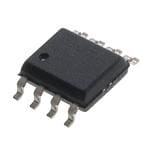
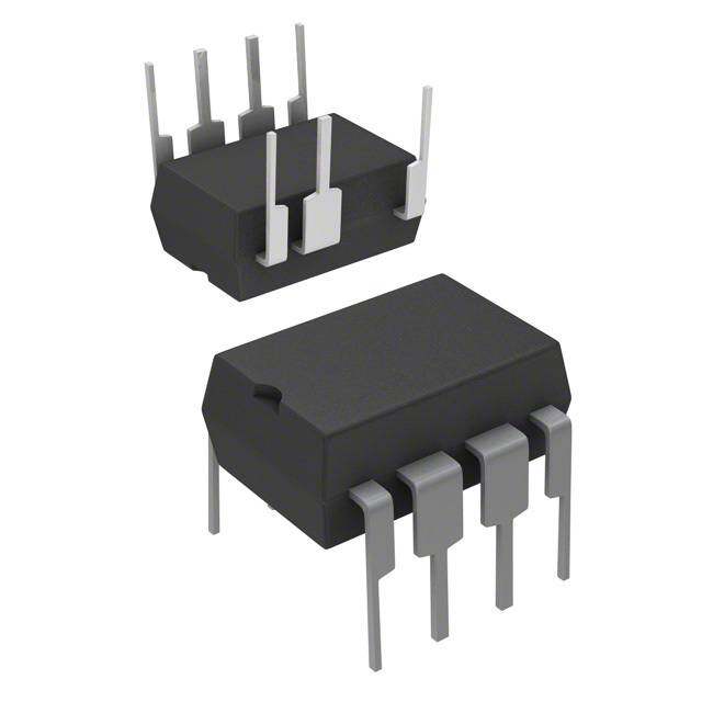
| 描述 | IC REG CTRLR BST FLYBK PWM 8SOIC |
| 产品分类 | |
| 品牌 | Texas Instruments |
| 数据手册 | |
| 产品图片 |
|
| 产品型号 | UCC2813QDR-2Q1 |
| PCN组件/产地 | |
| PWM类型 | 电流模式 |
| rohs | 无铅 / 符合限制有害物质指令(RoHS)规范要求 |
| 产品系列 | - |
| 倍增器 | 无 |
| 其它名称 | 296-23447-1 |
| 分频器 | 无 |
| 包装 | 剪切带 (CT) |
| 升压 | 是 |
| 占空比 | 100% |
| 反向 | 无 |
| 反激式 | 是 |
| 封装/外壳 | 8-SOIC(0.154",3.90mm 宽) |
| 工作温度 | -40°C ~ 125°C |
| 标准包装 | 1 |
| 电压-电源 | 8.3 V ~ 10 V |
| 输出数 | 1 |
| 降压 | 无 |
| 隔离式 | 无 |
| 频率-最大值 | 1MHz |


- 商务部:美国ITC正式对集成电路等产品启动337调查
- 曝三星4nm工艺存在良率问题 高通将骁龙8 Gen1或转产台积电
- 太阳诱电将投资9.5亿元在常州建新厂生产MLCC 预计2023年完工
- 英特尔发布欧洲新工厂建设计划 深化IDM 2.0 战略
- 台积电先进制程称霸业界 有大客户加持明年业绩稳了
- 达到5530亿美元!SIA预计今年全球半导体销售额将创下新高
- 英特尔拟将自动驾驶子公司Mobileye上市 估值或超500亿美元
- 三星加码芯片和SET,合并消费电子和移动部门,撤换高东真等 CEO
- 三星电子宣布重大人事变动 还合并消费电子和移动部门
- 海关总署:前11个月进口集成电路产品价值2.52万亿元 增长14.8%


PDF Datasheet 数据手册内容提取
(cid:26) (cid:1)(cid:2)(cid:2)(cid:3)(cid:4)(cid:5)(cid:6)(cid:7)(cid:8)(cid:9)(cid:7)(cid:5)(cid:9)(cid:7)(cid:3)(cid:9)(cid:7)(cid:6)(cid:9)(cid:7)(cid:10)(cid:9)(cid:7)(cid:11)(cid:7)(cid:12)(cid:5) (cid:13)(cid:14)(cid:15)(cid:7)(cid:16)(cid:14)(cid:15)(cid:17)(cid:18) (cid:19)(cid:20)(cid:2)(cid:21)(cid:14)(cid:22) (cid:2)(cid:1)(cid:18)(cid:18)(cid:17)(cid:23)(cid:24)(cid:7)(cid:21)(cid:14)(cid:25)(cid:17) (cid:16)(cid:15)(cid:21) SGLS245D − MAY 2004 − REVISED APRIL 2008 (cid:1) (cid:1) Qualified for Automotive Applications Internal Leading-Edge Blanking of the (cid:1) ESD Protection Exceeds 200 V Using Current Sense Signal (cid:1) Machine Model (C = 200 pF, R = 0) 1-A Totem-Pole Output (cid:1) 100-µA Typical Starting Supply Current (cid:1) 70-ns Typical Response From (cid:1) 500-µA Typical Operating Supply Current Current-Sense to Gate Drive Output (cid:1) Operation to 1 MHz (cid:1) 1.5% Tolerance Voltage Reference (cid:1) Internal Soft Start (cid:1) Same Pinout as UC3802, UC3842, and (cid:1) UC3842A Internal Fault Soft Start description The UCC2813-0/-1/-2/-3/-4/-5 family of high-speed low-power integrated circuits contain all of the control and drive components required for off-line and dc-to-dc fixed-frequency current-mode switching power supplies with minimal parts count. These devices have the same pin configuration as the UC2842/3/4/5 family and also offer the added features of internal full-cycle soft start and internal leading-edge blanking of the current-sense input. The UCC2813-0/-1/-2/-3/-4/-5 family offers choice of maximum duty cycle and critical voltage levels. Lower reference parts, such as the UCC2813-3 and UCC2813-5, fit best into battery-operated systems, while the higher reference and the higher undervoltage lockout (UVLO) hysteresis of the UCC2813-2 and UCC2813-4 make these ideal choices for use in off-line power supplies. The UCC2813-x series is specified for the automotive temperature range of −40(cid:2)C to 125(cid:2)C. PART NUMBER MAXIMUM DUTY CYCLE REFERENCE VOLTAGE TURN-ON THRESHOLD TURN-OFF THRESHOLD UCC2813-0 100% 5 V 7.2 V 6.9 V UCC2813-1 50% 5 V 9.4 V 7.4 V UCC2813-2 100% 5 V 12.5 V 8.3 V UCC2813-3 100% 4 V 4.1 V 3.6 V UCC2813-4 50% 5 V 12.5 V 8.3 V UCC2813-5 50% 4 V 4.1 V 3.6 V Please be aware that an important notice concerning availability, standard warranty, and use in critical applications of TexasInstruments semiconductor products and disclaimers thereto appears at the end of this data sheet. (cid:16)(cid:18)(cid:14)(cid:25)(cid:1)(cid:2)(cid:24)(cid:20)(cid:14)(cid:23) (cid:25)(cid:27)(cid:24)(cid:27) (cid:28)(cid:29)(cid:30)(cid:31)!"#$(cid:28)(cid:31)(cid:29) (cid:28)% &’!!((cid:29)$ #% (cid:31)(cid:30) )’*+(cid:28)&#$(cid:28)(cid:31)(cid:29) ,#$(- Copyright 2008 Texas Instruments Incorporated (cid:16)!(cid:31),’&$% &(cid:31)(cid:29)(cid:30)(cid:31)!" $(cid:31) %)(&(cid:28)(cid:30)(cid:28)&#$(cid:28)(cid:31)(cid:29)% )(! $.( $(!"% (cid:31)(cid:30) (cid:24)(/#% (cid:20)(cid:29)%$!’"((cid:29)$% %$#(cid:29),#!, 0#!!#(cid:29)$1- (cid:16)!(cid:31),’&$(cid:28)(cid:31)(cid:29) )!(cid:31)&(%%(cid:28)(cid:29)2 ,(cid:31)(% (cid:29)(cid:31)$ (cid:29)(&(%%#!(cid:28)+1 (cid:28)(cid:29)&+’,( $(%$(cid:28)(cid:29)2 (cid:31)(cid:30) #++ )#!#"($(!%- POST OFFICE BOX 655303 • DALLAS, TEXAS 75265 1
(cid:1)(cid:2)(cid:2)(cid:3)(cid:4)(cid:5)(cid:6)(cid:7)(cid:8)(cid:9)(cid:7)(cid:5)(cid:9)(cid:7)(cid:3)(cid:9)(cid:7)(cid:6)(cid:9)(cid:7)(cid:10)(cid:9)(cid:7)(cid:11)(cid:7)(cid:12)(cid:5) (cid:26) (cid:13)(cid:14)(cid:15)(cid:7)(cid:16)(cid:14)(cid:15)(cid:17)(cid:18) (cid:19)(cid:20)(cid:2)(cid:21)(cid:14)(cid:22) (cid:2)(cid:1)(cid:18)(cid:18)(cid:17)(cid:23)(cid:24)(cid:7)(cid:21)(cid:14)(cid:25)(cid:17) (cid:16)(cid:15)(cid:21) SGLS245D − MAY 2004 − REVISED APRIL 2008 block diagram − − − AVAILABLE OPTIONS†‡ D PACKAGE (TOP VIEW) ORDERABLE PART TA NUMBER COMP 1 8 REF UCC2813QDR-0Q1 FB 2 7 VCC UCC2813QDR-1Q1 CS 3 6 OUT UCC2813QDR-2Q1 RC 4 5 GND −−4400(cid:2)CC ttoo 112255(cid:2)CC UCC2813QDR-3Q1 UCC2813QDR-4Q1 TSSOP-8 PW PACKAGE UCC2813QDR-5Q1 (TOP VIEW) UCC2813QPWR-3Q1 †For the most current package and ordering COMP 1 8 REF information, see the Package Option Addendum at FB 2 7 VCC the end of this document, or see the TI web site at CS 3 6 OUT www.ti.com. RC 4 5 GND ‡Package drawings, thermal data, and symbolization are available at www.ti.com/packaging. 2 POST OFFICE BOX 655303 • DALLAS, TEXAS 75265
(cid:26) (cid:1)(cid:2)(cid:2)(cid:3)(cid:4)(cid:5)(cid:6)(cid:7)(cid:8)(cid:9)(cid:7)(cid:5)(cid:9)(cid:7)(cid:3)(cid:9)(cid:7)(cid:6)(cid:9)(cid:7)(cid:10)(cid:9)(cid:7)(cid:11)(cid:7)(cid:12)(cid:5) (cid:13)(cid:14)(cid:15)(cid:7)(cid:16)(cid:14)(cid:15)(cid:17)(cid:18) (cid:19)(cid:20)(cid:2)(cid:21)(cid:14)(cid:22) (cid:2)(cid:1)(cid:18)(cid:18)(cid:17)(cid:23)(cid:24)(cid:7)(cid:21)(cid:14)(cid:25)(cid:17) (cid:16)(cid:15)(cid:21) SGLS245D − MAY 2004 − REVISED APRIL 2008 ordering information UCC2813- Q D R 0 Product Option 0 through 5 Tape and Reel Indicator Package D = Plastic SOIC, PW = Plastic TSSOP Automotive Temperature Range Indicator absolute maximum ratings over operating free-air temperature range (unless otherwise noted)†‡ V voltage (cid:3) . . . . . . . . . . . . . . . . . . . . . . . . . . . . . . . . . . . . . . . . . . . . . . . . . . . . . . . . . . . . . . . . . . . . . . . . . . . . . 12 V CC V current (cid:3) . . . . . . . . . . . . . . . . . . . . . . . . . . . . . . . . . . . . . . . . . . . . . . . . . . . . . . . . . . . . . . . . . . . . . . . . . . . 30 mA CC Output current, IO . . . . . . . . . . . . . . . . . . . . . . . . . . . . . . . . . . . . . . . . . . . . . . . . . . . . . . . . . . . . . . . . . . . . . . . . . ±1 A Output energy (capacitive load) . . . . . . . . . . . . . . . . . . . . . . . . . . . . . . . . . . . . . . . . . . . . . . . . . . . . . . . . . . . . . 20 µJ Analog inputs (FB, CS) . . . . . . . . . . . . . . . . . . . . . . . . . . . . . . . . . . . . . . . . . . . . . . . . . . . . . . . . . . . . −0.3 V to 6.3 V Power dissipation at T < +25(cid:2)C (D package) . . . . . . . . . . . . . . . . . . . . . . . . . . . . . . . . . . . . . . . . . . . . . . 0.65 W A Storage temperature range, T . . . . . . . . . . . . . . . . . . . . . . . . . . . . . . . . . . . . . . . . . . . . . . . . . . . . −65(cid:2)C to 150(cid:2)C stg Lead temperature soldering 1,6 mm (1/16 inch) from case for 10 seconds . . . . . . . . . . . . . . . . . . . . . . . 300(cid:2)C †Stresses beyond those listed under “absolute maximum ratings” may cause permanent damage to the device. These are stress ratings only, and functional operation of the device at these or any other conditions beyond those indicated under “recommended operating conditions” is not implied. Exposure to absolute-maximum-rated conditions for extended periods may affect device reliability. ‡Unless otherwise indicated, voltages are reference to ground and currents are positive into and negative out of the specified terminals. (cid:3)In normal operation VCC is powered through a current limiting resistor. Absolute maximum of 12 V applies when VCC is driven from a low impedance source such that ICC does not exceed 30 mA (which includes gate drive current requirement). electrical characteristics T = −40(cid:2)C to 125(cid:2)C, V = 10 V (see Note 1), RT = 100 kΩ from REF to A CC RC, CT = 330 pF from RC to GND, 0.1-F capacitor from V to GND, 0.1-F capacitor from V to CC REF GND, and TA = TJ (unless otherwise noted) PARAMETER TEST CONDITIONS MIN TYP MAX UNIT Reference Section UCC2813-0/-1/-2/-4 4.925 5 5.075 (cid:2)(cid:2) OOuuttppuutt vvoollttaaggee TTJJ == 2255 CC,, II == 00..22 mmAA VV UCC2813-3/-5 3.94 4 4.06 Load regulation voltage I = 0.2 mA to 5 mA 10 30 mV UCC2813-0/-1/-2/-4 4.84 5 5.1 TToottaall vvaarriiaattiioonn vvoollttaaggee SSeeee NNoottee 55 VV UCC2813-3/-5 3.84 4 4.08 f = 10 Hz to 10 kHz, Output noise voltage See Note 7 TJ = 25(cid:2)C 70 µV 1000 hours, Long term stability See Note 7 TA = 125(cid:2)C 5 mV Output short-circuit current −5 −35 mA POST OFFICE BOX 655303 • DALLAS, TEXAS 75265 3
(cid:1)(cid:2)(cid:2)(cid:3)(cid:4)(cid:5)(cid:6)(cid:7)(cid:8)(cid:9)(cid:7)(cid:5)(cid:9)(cid:7)(cid:3)(cid:9)(cid:7)(cid:6)(cid:9)(cid:7)(cid:10)(cid:9)(cid:7)(cid:11)(cid:7)(cid:12)(cid:5) (cid:26) (cid:13)(cid:14)(cid:15)(cid:7)(cid:16)(cid:14)(cid:15)(cid:17)(cid:18) (cid:19)(cid:20)(cid:2)(cid:21)(cid:14)(cid:22) (cid:2)(cid:1)(cid:18)(cid:18)(cid:17)(cid:23)(cid:24)(cid:7)(cid:21)(cid:14)(cid:25)(cid:17) (cid:16)(cid:15)(cid:21) SGLS245D − MAY 2004 − REVISED APRIL 2008 electrical characteristics T = −40(cid:2)C to 125(cid:2)C, V = 10 V (see Note 1), RT = 100 kΩ from REF to A CC RC, CT = 330 pF from RC to GND, 0.1 F capacitor from V to GND, 0.1 F capacitor from V to GND CC REF and TA = TJ (unless otherwise noted) PARAMETER TEST CONDITIONS MIN TYP MAX UNIT Oscillator Section UCC2813-0/-1/-2/-4 40 46 52 OOsscciillllaattoorr ffrreeqquueennccyy SSeeee NNoottee 22 kkHHzz UCC2813-3/-5 26 31 36 Temperature stability See Note 7 2.5 % Amplitude, peak to peak 2.25 2.4 2.55 V Oscillator peak voltage 2.45 V Error Amplifier Section COMP = 2.5 V UCC2813-0/-1/-2/-4 2.42 2.5 2.56 IInnppuutt vvoollttaaggee VV COMP = 2.0 V UCC2813-3/-5 1.92 2 2.05 Input bias current −2 2 µA Open loop voltage gain 60 80 dB COMP sink current FB = 2.7 V, COMP = 1.1 V 0.3 3.5 mA COMP source current FB = 1.8 V, COMP = REF − 1.2 V −0.2 −0.5 −0.8 mA Gain bandwidth product See Note 7 2 MHz PWM Section UCC2813-0/-2/-3 97 99 100 MMaaxxiimmuumm dduuttyy ccyyccllee %% UCC2813-1/-4/-5 48 49 50 Minimum duty cycle COMP = 0 V 0 % Current Sense Section Gain See Note 3 1.1 1.65 1.8 V/V Maximum input signal COMP = 5 V, See Note 4 0.9 1 1.1 V Input bias current −200 200 nA CS blank time 50 100 150 ns Over-current threshold voltage 1.32 1.55 1.7 V COMP to CS offset voltage CS = 0 V 0.45 0.9 1.35 V Output Section (OUT) IOUT = 20 mA All parts 0.1 0.4 IOUT = 200 mA All parts 0.35 0.9 LLooww--lleevveell oouuttppuutt vvoollttaaggee VV IOUT = 50 mA, VCC = 5 V UCC2813-3/-5 0.15 0.4 IOUT = 20 mA, VCC = 0 V All parts 0.7 1.2 IOUT = −20 mA All parts 0.15 0.4 HHiigghh--lleevveell oouuttppuutt vvoollttaaggee,, VVSSAATT ((VVCCCC −− OOUUTT)) IOUT = −200 mA All parts 1 1.9 VV IOUT = −50 mA, VCC = 5 V UCC2813-3/-5 0.4 0.9 Rise time CL = 1 nF 41 70 ns Fall time CL = 1 nF 44 75 ns 4 POST OFFICE BOX 655303 • DALLAS, TEXAS 75265
(cid:26) (cid:1)(cid:2)(cid:2)(cid:3)(cid:4)(cid:5)(cid:6)(cid:7)(cid:8)(cid:9)(cid:7)(cid:5)(cid:9)(cid:7)(cid:3)(cid:9)(cid:7)(cid:6)(cid:9)(cid:7)(cid:10)(cid:9)(cid:7)(cid:11)(cid:7)(cid:12)(cid:5) (cid:13)(cid:14)(cid:15)(cid:7)(cid:16)(cid:14)(cid:15)(cid:17)(cid:18) (cid:19)(cid:20)(cid:2)(cid:21)(cid:14)(cid:22) (cid:2)(cid:1)(cid:18)(cid:18)(cid:17)(cid:23)(cid:24)(cid:7)(cid:21)(cid:14)(cid:25)(cid:17) (cid:16)(cid:15)(cid:21) SGLS245D − MAY 2004 − REVISED APRIL 2008 electrical characteristics T = −40(cid:2)C to 125(cid:2)C, V = 10 V (see Note 1), RT = 100 kΩ from REF to A CC RC, CT = 330 pF from RC to GND, 0.1 F capacitor from V to GND, 0.1 F capacitor from V to GND, CC REF and TA = TJ (unless otherwise noted) PARAMETER TEST CONDITIONS MIN TYP MAX UNIT Undervoltage Lockout Section UCC2813-0 6.6 7.2 7.8 UCC2813-1 8.6 9.4 10.2 SSttaarrtt tthhrreesshhoolldd SSeeee NNoottee 66 VV UCC2813-2/-4 11.5 12.5 13.5 UCC2813-3/-5 3.7 4.1 4.5 UCC2813-0 6.3 6.9 7.5 UCC2813-1 6.8 7.4 8 SSttoopp tthhrreesshhoolldd SSeeee NNoottee 66 VV UCC2813-2/-4 7.6 8.3 9 UCC2813-3/-5 3.2 3.6 4 UCC2813-0 0.12 0.3 0.48 UCC2813-1 1.6 2 2.4 SSttaarrtt ttoo ssttoopp hhyysstteerreessiiss VV UCC2813-2/-4 3.5 4.2 5.1 UCC2813-3/-5 0.2 0.5 0.8 Soft-Start Section COMP rise time FB = 1.8 V, Rise from 0.5 V to REF − 1 V 4 10 ms Overall Start-up current VCC < Start hreshold 0.1 0.23 mA Operating supply current FB = 0 V, CS = 0 V, RC = 0 V 0.5 1.2 mA VCC internal zener voltage ICC = 10 mA, See Notes 6 and 8 12 13.5 15 V VCC internal zener voltage minus start See Note 6 UCC2813-2/-4 0.5 1.0 V threshold voltage NOTES: 1. Adjust VCC above the start threshold before setting at 10 V. 2. Oscillator frequency for the UCC2813-0, UCC2813-2, and UCC2813-3 is the output frequency. Oscillator frequency for the UCC2813-1, UCC2813-4, and UCC2813-5 is twice the output frequency. 3. Gain is defined by: (cid:1)VCOMP 0 (cid:1) VCS (cid:1) 0.8 V. A = (cid:1)VCS 4. Parameter measured at trip point of latch with pin 2 at 0 V. 5. Total variation includes temperature stability and load regulation. 6. Start threshold, stop threshold, and Zener shunt thresholds track one another. 7. Not production tested 8. The device is fully operating in clamp mode as the forcing current is higher than the normal operating supply current. POST OFFICE BOX 655303 • DALLAS, TEXAS 75265 5
(cid:1)(cid:2)(cid:2)(cid:3)(cid:4)(cid:5)(cid:6)(cid:7)(cid:8)(cid:9)(cid:7)(cid:5)(cid:9)(cid:7)(cid:3)(cid:9)(cid:7)(cid:6)(cid:9)(cid:7)(cid:10)(cid:9)(cid:7)(cid:11)(cid:7)(cid:12)(cid:5) (cid:26) (cid:13)(cid:14)(cid:15)(cid:7)(cid:16)(cid:14)(cid:15)(cid:17)(cid:18) (cid:19)(cid:20)(cid:2)(cid:21)(cid:14)(cid:22) (cid:2)(cid:1)(cid:18)(cid:18)(cid:17)(cid:23)(cid:24)(cid:7)(cid:21)(cid:14)(cid:25)(cid:17) (cid:16)(cid:15)(cid:21) SGLS245D − MAY 2004 − REVISED APRIL 2008 detailed terminal descriptions COMP COMP is the output of the error amplifier and the input of the PWM comparator. Unlike other devices, the error amplifier in the UCC2813 family is a true, low output-impedance, 2-MHz operational amplifier. As such, the COMP terminal can both source and sink current. However, the error amplifier is internally current limited, so that one can command zero duty cycle by externally forcing COMP to GND. The UCC2813 family features built-in full-cycle soft start. Soft start is implemented as a clamp on the maximum COMP voltage. CS CS is the input to the current sense comparators. The UCC2813 family has two different current sense comparators: the PWM comparator and an overcurrent comparator. The UCC2813 family contains digital current sense filtering, which disconnects the CS terminal from the current sense comparator during the 100 ns interval immediately following the rising edge of the OUT pin. This digital filtering, also called leading-edge blanking, means that in most applications, no analog filtering (RC filter) is required on CS. Compared to an external RC filter technique, the leading-edge blanking provides a smaller effective CS to OUT propagation delay. Note, however, that the minimum non-zero on time of the OUT signal is directly affected by the leading-edge blanking and the CS to OUT propagation delay. The overcurrent comparator is only intended for fault sensing, and exceeding the overcurrent threshold causes a soft start cycle. FB FB is the inverting input of the error amplifier. For best stability, keep FB lead length as short as possible and FB stray capacitance as small as possible. GND GND is reference ground and power ground for all functions on this part. OUT OUT is the output of a high-current power driver capable of driving the gate of a power MOSFET with peak currents exceeding (cid:2)750 mA. OUT is actively held low when V is below the UVLO threshold. CC The high-current power driver consists of FET output devices, which can switch all of the way to GND and all of the way to V . The output stage also provides a low impedance to overshoot and undershoot. This means CC that, in many cases, external Schottky clamp diodes are not required. 6 POST OFFICE BOX 655303 • DALLAS, TEXAS 75265
(cid:26) (cid:1)(cid:2)(cid:2)(cid:3)(cid:4)(cid:5)(cid:6)(cid:7)(cid:8)(cid:9)(cid:7)(cid:5)(cid:9)(cid:7)(cid:3)(cid:9)(cid:7)(cid:6)(cid:9)(cid:7)(cid:10)(cid:9)(cid:7)(cid:11)(cid:7)(cid:12)(cid:5) (cid:13)(cid:14)(cid:15)(cid:7)(cid:16)(cid:14)(cid:15)(cid:17)(cid:18) (cid:19)(cid:20)(cid:2)(cid:21)(cid:14)(cid:22) (cid:2)(cid:1)(cid:18)(cid:18)(cid:17)(cid:23)(cid:24)(cid:7)(cid:21)(cid:14)(cid:25)(cid:17) (cid:16)(cid:15)(cid:21) SGLS245D − MAY 2004 − REVISED APRIL 2008 detailed descriptions (continued) RC RC is the oscillator timing pin. For fixed frequency operation, set timing capacitor charging current by connecting a resistor from REF to RC. Set frequency by connecting timing capacitor from RC to GND. For best perfomance, keep the timing capacitor lead to GND as short and direct as possible. If possible, use separate ground traces for the timing capacitor and all other functions. The frequency of oscillation can be estimated with the following equations: UCC2813−0(cid:3)1(cid:3)2(cid:3)4: F(cid:4) 1.5 R(cid:5)C UCC2813−3(cid:3)UCC2813−5: F(cid:4) 1.0 R(cid:5)C (1) where frequency is in Hz, resistance is in ohms, and capacitance is in farads. The recommended range of the timing resistors is between 10 kΩ and 200 kΩ and the timing capacitor is 100 pF to 1000 pF. Never use a timing resistor less than 10 k. To prevent noise problems, bypass V to GND with a ceramic capacitor as close to the V pin as possible. CC CC An electrolytic capacitor may also be used in addition to the ceramic capacitor. voltage reference (REF) REF is the voltage reference for the error amplifier and also for many other functions on the IC. REF is also used as the logic power supply for high-speed switching logic on the IC. When V is greater than 1 V and less than the UVLO threshold, REF is pulled to ground through a 5-kΩ resistor. CC This means that REF can be used as a logic output indicating power system status. It is important for reference stability that REF is bypassed to GND with a ceramic capacitor as close to the pin as possible. An electrolytic capacitor may also be used in addition to the ceramic capacitor. A minimum of 0.1-µF ceramic capacitor is required. Additional REF bypassing is required for external loads greater than 2.5 mA on the reference. To prevent noise problems with high-speed switching transients, bypass REF to ground with a ceramic capacitor close to the IC package. power (V ) CC V is the power input connection for this device. In normal operation, V is powered through a current-limiting CC CC resistor. Although quiescent V current is low, total supply current will be higher, depending on OUT current. CC Total V current is the sum of quiescent V current and the average OUT current. Knowing the operating CC CC frequency and the MOSFET gate charge (Q ), average OUT current can be calculated from: g I (cid:4)Q (cid:5)F. OUT g (2) POST OFFICE BOX 655303 • DALLAS, TEXAS 75265 7
(cid:1)(cid:2)(cid:2)(cid:3)(cid:4)(cid:5)(cid:6)(cid:7)(cid:8)(cid:9)(cid:7)(cid:5)(cid:9)(cid:7)(cid:3)(cid:9)(cid:7)(cid:6)(cid:9)(cid:7)(cid:10)(cid:9)(cid:7)(cid:11)(cid:7)(cid:12)(cid:5) (cid:26) (cid:13)(cid:14)(cid:15)(cid:7)(cid:16)(cid:14)(cid:15)(cid:17)(cid:18) (cid:19)(cid:20)(cid:2)(cid:21)(cid:14)(cid:22) (cid:2)(cid:1)(cid:18)(cid:18)(cid:17)(cid:23)(cid:24)(cid:7)(cid:21)(cid:14)(cid:25)(cid:17) (cid:16)(cid:15)(cid:21) SGLS245D − MAY 2004 − REVISED APRIL 2008 PARAMETER MEASUREMENT INFORMATION Oscillator Error Amplifier Gain/Phase Response REF 8 0.2 V R Q R T S RC 4 2.5 V C T The UCC2813-0/-1/-2/-3/-4/-5 oscillator generates a sawtooth waveform on RC. The rise time is set by the time constant of RT and CT. The fall time is set by CT and an internal transistor on-resistance of approximately 125. During the fall time, the output is off and the maximum duty cycle is reduced below 50% or 100% depending on the part number. Larger timing capacitors increase the discharge time and reduce the maximum duty cycle and frequency. Figure 1 Figure 2 UCC2813-3/5 V UCC2813-0/1/2/4 Oscillator Frequency REF vs vs VCC RT and CT I = 0.5 mA LOAD Figure 3 Figure 4 8 POST OFFICE BOX 655303 • DALLAS, TEXAS 75265
(cid:26) (cid:1)(cid:2)(cid:2)(cid:3)(cid:4)(cid:5)(cid:6)(cid:7)(cid:8)(cid:9)(cid:7)(cid:5)(cid:9)(cid:7)(cid:3)(cid:9)(cid:7)(cid:6)(cid:9)(cid:7)(cid:10)(cid:9)(cid:7)(cid:11)(cid:7)(cid:12)(cid:5) (cid:13)(cid:14)(cid:15)(cid:7)(cid:16)(cid:14)(cid:15)(cid:17)(cid:18) (cid:19)(cid:20)(cid:2)(cid:21)(cid:14)(cid:22) (cid:2)(cid:1)(cid:18)(cid:18)(cid:17)(cid:23)(cid:24)(cid:7)(cid:21)(cid:14)(cid:25)(cid:17) (cid:16)(cid:15)(cid:21) SGLS245D − MAY 2004 − REVISED APRIL 2008 UCC2813-3/5 Oscillator Frequency UCC2813-0/2/3 Maximum Duty Cycle vs vs RT and CT Oscillator Frequency Figure 5 Figure 6 UCC2813-1/4/5 Maximum Duty Cycle UCC2813-0 ICC vs vs Oscillator Frequency Oscillator Frequency Figure 8 Figure 7 POST OFFICE BOX 655303 • DALLAS, TEXAS 75265 9
(cid:1)(cid:2)(cid:2)(cid:3)(cid:4)(cid:5)(cid:6)(cid:7)(cid:8)(cid:9)(cid:7)(cid:5)(cid:9)(cid:7)(cid:3)(cid:9)(cid:7)(cid:6)(cid:9)(cid:7)(cid:10)(cid:9)(cid:7)(cid:11)(cid:7)(cid:12)(cid:5) (cid:26) (cid:13)(cid:14)(cid:15)(cid:7)(cid:16)(cid:14)(cid:15)(cid:17)(cid:18) (cid:19)(cid:20)(cid:2)(cid:21)(cid:14)(cid:22) (cid:2)(cid:1)(cid:18)(cid:18)(cid:17)(cid:23)(cid:24)(cid:7)(cid:21)(cid:14)(cid:25)(cid:17) (cid:16)(cid:15)(cid:21) SGLS245D − MAY 2004 − REVISED APRIL 2008 UCC2813-5 ICC Dead Time vs vs Oscillator Frequency C T R = 100 k(cid:1) T Figure 9 Figure 10 COMP to CS Offset vs Temperature CS = 0 V Figure 11 10 POST OFFICE BOX 655303 • DALLAS, TEXAS 75265
PACKAGE OPTION ADDENDUM www.ti.com 6-Feb-2020 PACKAGING INFORMATION Orderable Device Status Package Type Package Pins Package Eco Plan Lead/Ball Finish MSL Peak Temp Op Temp (°C) Device Marking Samples (1) Drawing Qty (2) (6) (3) (4/5) UCC2813QDR-0Q1 ACTIVE SOIC D 8 2500 Green (RoHS NIPDAU Level-1-260C-UNLIM -40 to 125 (2813-0, 2813-0Q1) & no Sb/Br) UCC2813QDR-1Q1 ACTIVE SOIC D 8 2500 Green (RoHS NIPDAU Level-1-260C-UNLIM -40 to 125 (2813-1, 2813-1Q1) & no Sb/Br) UCC2813QDR-2Q1 ACTIVE SOIC D 8 2500 Green (RoHS NIPDAU Level-1-260C-UNLIM -40 to 125 (2813-2, 2813-2Q1) & no Sb/Br) UCC2813QDR-3Q1 ACTIVE SOIC D 8 2500 Green (RoHS NIPDAU Level-1-260C-UNLIM -40 to 125 (2813-3, 2813-3Q1) & no Sb/Br) UCC2813QDR-4Q1 ACTIVE SOIC D 8 2500 Green (RoHS NIPDAU Level-1-260C-UNLIM -40 to 125 (2813-4, 2813-4Q1) & no Sb/Br) UCC2813QDR-5Q1 ACTIVE SOIC D 8 2500 Green (RoHS NIPDAU Level-1-260C-UNLIM -40 to 125 (2813-5, 2813-5Q1) & no Sb/Br) UCC2813QPWR-3Q1 ACTIVE TSSOP PW 8 2000 Green (RoHS NIPDAU Level-1-260C-UNLIM -40 to 125 28133Q & no Sb/Br) (1) The marketing status values are defined as follows: ACTIVE: Product device recommended for new designs. LIFEBUY: TI has announced that the device will be discontinued, and a lifetime-buy period is in effect. NRND: Not recommended for new designs. Device is in production to support existing customers, but TI does not recommend using this part in a new design. PREVIEW: Device has been announced but is not in production. Samples may or may not be available. OBSOLETE: TI has discontinued the production of the device. (2) RoHS: TI defines "RoHS" to mean semiconductor products that are compliant with the current EU RoHS requirements for all 10 RoHS substances, including the requirement that RoHS substance do not exceed 0.1% by weight in homogeneous materials. Where designed to be soldered at high temperatures, "RoHS" products are suitable for use in specified lead-free processes. TI may reference these types of products as "Pb-Free". RoHS Exempt: TI defines "RoHS Exempt" to mean products that contain lead but are compliant with EU RoHS pursuant to a specific EU RoHS exemption. Green: TI defines "Green" to mean the content of Chlorine (Cl) and Bromine (Br) based flame retardants meet JS709B low halogen requirements of <=1000ppm threshold. Antimony trioxide based flame retardants must also meet the <=1000ppm threshold requirement. (3) MSL, Peak Temp. - The Moisture Sensitivity Level rating according to the JEDEC industry standard classifications, and peak solder temperature. (4) There may be additional marking, which relates to the logo, the lot trace code information, or the environmental category on the device. (5) Multiple Device Markings will be inside parentheses. Only one Device Marking contained in parentheses and separated by a "~" will appear on a device. If a line is indented then it is a continuation of the previous line and the two combined represent the entire Device Marking for that device. Addendum-Page 1
PACKAGE OPTION ADDENDUM www.ti.com 6-Feb-2020 (6) Lead/Ball Finish - Orderable Devices may have multiple material finish options. Finish options are separated by a vertical ruled line. Lead/Ball Finish values may wrap to two lines if the finish value exceeds the maximum column width. Important Information and Disclaimer:The information provided on this page represents TI's knowledge and belief as of the date that it is provided. TI bases its knowledge and belief on information provided by third parties, and makes no representation or warranty as to the accuracy of such information. Efforts are underway to better integrate information from third parties. TI has taken and continues to take reasonable steps to provide representative and accurate information but may not have conducted destructive testing or chemical analysis on incoming materials and chemicals. TI and TI suppliers consider certain information to be proprietary, and thus CAS numbers and other limited information may not be available for release. In no event shall TI's liability arising out of such information exceed the total purchase price of the TI part(s) at issue in this document sold by TI to Customer on an annual basis. OTHER QUALIFIED VERSIONS OF UCC2813-0-Q1, UCC2813-1-Q1, UCC2813-2-Q1, UCC2813-3-Q1, UCC2813-4-Q1, UCC2813-5-Q1 : •Catalog: UCC2813-0, UCC2813-1, UCC2813-2, UCC2813-3, UCC2813-4, UCC2813-5 NOTE: Qualified Version Definitions: •Catalog - TI's standard catalog product Addendum-Page 2
PACKAGE MATERIALS INFORMATION www.ti.com 29-Apr-2016 TAPE AND REEL INFORMATION *Alldimensionsarenominal Device Package Package Pins SPQ Reel Reel A0 B0 K0 P1 W Pin1 Type Drawing Diameter Width (mm) (mm) (mm) (mm) (mm) Quadrant (mm) W1(mm) UCC2813QDR-0Q1 SOIC D 8 2500 330.0 12.4 6.4 5.2 2.1 8.0 12.0 Q1 UCC2813QDR-1Q1 SOIC D 8 2500 330.0 12.4 6.4 5.2 2.1 8.0 12.0 Q1 UCC2813QDR-2Q1 SOIC D 8 2500 330.0 12.4 6.4 5.2 2.1 8.0 12.0 Q1 UCC2813QDR-3Q1 SOIC D 8 2500 330.0 12.4 6.4 5.2 2.1 8.0 12.0 Q1 UCC2813QDR-4Q1 SOIC D 8 2500 330.0 12.4 6.4 5.2 2.1 8.0 12.0 Q1 UCC2813QDR-5Q1 SOIC D 8 2500 330.0 12.4 6.4 5.2 2.1 8.0 12.0 Q1 UCC2813QPWR-3Q1 TSSOP PW 8 2000 330.0 12.4 7.0 3.6 1.6 8.0 12.0 Q1 PackMaterials-Page1
PACKAGE MATERIALS INFORMATION www.ti.com 29-Apr-2016 *Alldimensionsarenominal Device PackageType PackageDrawing Pins SPQ Length(mm) Width(mm) Height(mm) UCC2813QDR-0Q1 SOIC D 8 2500 367.0 367.0 35.0 UCC2813QDR-1Q1 SOIC D 8 2500 367.0 367.0 35.0 UCC2813QDR-2Q1 SOIC D 8 2500 367.0 367.0 35.0 UCC2813QDR-3Q1 SOIC D 8 2500 367.0 367.0 35.0 UCC2813QDR-4Q1 SOIC D 8 2500 367.0 367.0 35.0 UCC2813QDR-5Q1 SOIC D 8 2500 367.0 367.0 35.0 UCC2813QPWR-3Q1 TSSOP PW 8 2000 367.0 367.0 35.0 PackMaterials-Page2
PACKAGE OUTLINE D0008A SOIC - 1.75 mm max height SCALE 2.800 SMALL OUTLINE INTEGRATED CIRCUIT C SEATING PLANE .228-.244 TYP [5.80-6.19] .004 [0.1] C A PIN 1 ID AREA 6X .050 [1.27] 8 1 2X .189-.197 [4.81-5.00] .150 NOTE 3 [3.81] 4X (0 -15 ) 4 5 8X .012-.020 B .150-.157 [0.31-0.51] .069 MAX [3.81-3.98] .010 [0.25] C A B [1.75] NOTE 4 .005-.010 TYP [0.13-0.25] 4X (0 -15 ) SEE DETAIL A .010 [0.25] .004-.010 0 - 8 [0.11-0.25] .016-.050 [0.41-1.27] DETAIL A (.041) TYPICAL [1.04] 4214825/C 02/2019 NOTES: 1. Linear dimensions are in inches [millimeters]. Dimensions in parenthesis are for reference only. Controlling dimensions are in inches. Dimensioning and tolerancing per ASME Y14.5M. 2. This drawing is subject to change without notice. 3. This dimension does not include mold flash, protrusions, or gate burrs. Mold flash, protrusions, or gate burrs shall not exceed .006 [0.15] per side. 4. This dimension does not include interlead flash. 5. Reference JEDEC registration MS-012, variation AA. www.ti.com
EXAMPLE BOARD LAYOUT D0008A SOIC - 1.75 mm max height SMALL OUTLINE INTEGRATED CIRCUIT 8X (.061 ) [1.55] SYMM SEE DETAILS 1 8 8X (.024) [0.6] SYMM (R.002 ) TYP [0.05] 5 4 6X (.050 ) [1.27] (.213) [5.4] LAND PATTERN EXAMPLE EXPOSED METAL SHOWN SCALE:8X SOLDER MASK SOLDER MASK METAL OPENING OPENING METAL UNDER SOLDER MASK EXPOSED METAL EXPOSED METAL .0028 MAX .0028 MIN [0.07] [0.07] ALL AROUND ALL AROUND NON SOLDER MASK SOLDER MASK DEFINED DEFINED SOLDER MASK DETAILS 4214825/C 02/2019 NOTES: (continued) 6. Publication IPC-7351 may have alternate designs. 7. Solder mask tolerances between and around signal pads can vary based on board fabrication site. www.ti.com
EXAMPLE STENCIL DESIGN D0008A SOIC - 1.75 mm max height SMALL OUTLINE INTEGRATED CIRCUIT 8X (.061 ) [1.55] SYMM 1 8 8X (.024) [0.6] SYMM (R.002 ) TYP [0.05] 5 4 6X (.050 ) [1.27] (.213) [5.4] SOLDER PASTE EXAMPLE BASED ON .005 INCH [0.125 MM] THICK STENCIL SCALE:8X 4214825/C 02/2019 NOTES: (continued) 8. Laser cutting apertures with trapezoidal walls and rounded corners may offer better paste release. IPC-7525 may have alternate design recommendations. 9. Board assembly site may have different recommendations for stencil design. www.ti.com
PACKAGE OUTLINE PW0008A TSSOP - 1.2 mm max height SCALE 2.800 SMALL OUTLINE PACKAGE C 6.6 TYP SEATING PLANE 6.2 PIN 1 ID A 0.1 C AREA 6X 0.65 8 1 3.1 2X 2.9 NOTE 3 1.95 4 5 0.30 8X 0.19 4.5 1.2 MAX B 0.1 C A B 4.3 NOTE 4 (0.15) TYP SEE DETAIL A 0.25 GAGE PLANE 0.15 0.75 0 - 8 0.05 0.50 DETAIL A TYPICAL 4221848/A 02/2015 NOTES: 1. All linear dimensions are in millimeters. Any dimensions in parenthesis are for reference only. Dimensioning and tolerancing per ASME Y14.5M. 2. This drawing is subject to change without notice. 3. This dimension does not include mold flash, protrusions, or gate burrs. Mold flash, protrusions, or gate burrs shall not exceed 0.15 mm per side. 4. This dimension does not include interlead flash. Interlead flash shall not exceed 0.25 mm per side. 5. Reference JEDEC registration MO-153, variation AA. www.ti.com
EXAMPLE BOARD LAYOUT PW0008A TSSOP - 1.2 mm max height SMALL OUTLINE PACKAGE 8X (1.5) 8X (0.45) SYMM (R0.05) 1 TYP 8 SYMM 6X (0.65) 5 4 (5.8) LAND PATTERN EXAMPLE SCALE:10X SOOPLEDNEINRG MASK METAL MSOELTDAEL RU NMDAESRK SOOPLEDNEINRG MASK 0.05 MAX 0.05 MIN ALL AROUND ALL AROUND NON SOLDER MASK SOLDER MASK DEFINED DEFINED SOLDER MASK DETAILS NOT TO SCALE 4221848/A 02/2015 NOTES: (continued) 6. Publication IPC-7351 may have alternate designs. 7. Solder mask tolerances between and around signal pads can vary based on board fabrication site. www.ti.com
EXAMPLE STENCIL DESIGN PW0008A TSSOP - 1.2 mm max height SMALL OUTLINE PACKAGE 8X (1.5) SYMM (R0.05) TYP 8X (0.45) 1 8 SYMM 6X (0.65) 5 4 (5.8) SOLDER PASTE EXAMPLE BASED ON 0.125 mm THICK STENCIL SCALE:10X 4221848/A 02/2015 NOTES: (continued) 8. Laser cutting apertures with trapezoidal walls and rounded corners may offer better paste release. IPC-7525 may have alternate design recommendations. 9. Board assembly site may have different recommendations for stencil design. www.ti.com
IMPORTANTNOTICEANDDISCLAIMER TI PROVIDES TECHNICAL AND RELIABILITY DATA (INCLUDING DATASHEETS), DESIGN RESOURCES (INCLUDING REFERENCE DESIGNS), APPLICATION OR OTHER DESIGN ADVICE, WEB TOOLS, SAFETY INFORMATION, AND OTHER RESOURCES “AS IS” AND WITH ALL FAULTS, AND DISCLAIMS ALL WARRANTIES, EXPRESS AND IMPLIED, INCLUDING WITHOUT LIMITATION ANY IMPLIED WARRANTIES OF MERCHANTABILITY, FITNESS FOR A PARTICULAR PURPOSE OR NON-INFRINGEMENT OF THIRD PARTY INTELLECTUAL PROPERTY RIGHTS. These resources are intended for skilled developers designing with TI products. You are solely responsible for (1) selecting the appropriate TI products for your application, (2) designing, validating and testing your application, and (3) ensuring your application meets applicable standards, and any other safety, security, or other requirements. These resources are subject to change without notice. TI grants you permission to use these resources only for development of an application that uses the TI products described in the resource. Other reproduction and display of these resources is prohibited. No license is granted to any other TI intellectual property right or to any third party intellectual property right. TI disclaims responsibility for, and you will fully indemnify TI and its representatives against, any claims, damages, costs, losses, and liabilities arising out of your use of these resources. TI’s products are provided subject to TI’s Terms of Sale (www.ti.com/legal/termsofsale.html) or other applicable terms available either on ti.com or provided in conjunction with such TI products. TI’s provision of these resources does not expand or otherwise alter TI’s applicable warranties or warranty disclaimers for TI products. Mailing Address: Texas Instruments, Post Office Box 655303, Dallas, Texas 75265 Copyright © 2020, Texas Instruments Incorporated