ICGOO在线商城 > 集成电路(IC) > PMIC - AC-DC 转换器,离线开关 > UCC2895PW
 Datasheet下载
- 型号: UCC2895PW
- 制造商: Texas Instruments
- 库位|库存: xxxx|xxxx
- 要求:
| 数量阶梯 | 香港交货 | 国内含税 |
| +xxxx | $xxxx | ¥xxxx |
查看当月历史价格
查看今年历史价格
UCC2895PW产品简介:
ICGOO电子元器件商城为您提供UCC2895PW由Texas Instruments设计生产,在icgoo商城现货销售,并且可以通过原厂、代理商等渠道进行代购。 UCC2895PW价格参考¥30.87-¥58.53。Texas InstrumentsUCC2895PW封装/规格:PMIC - AC-DC 转换器,离线开关, Converter Offline Full-Bridge Topology 1MHz 20-TSSOP。您可以下载UCC2895PW参考资料、Datasheet数据手册功能说明书,资料中有UCC2895PW 详细功能的应用电路图电压和使用方法及教程。
UCC2895PW 是 Texas Instruments(德州仪器)推出的一款 PMIC - AC-DC 转换器,属于离线开关类别。该器件主要应用于需要高效、低待机功耗的电源系统中,以下是其典型应用场景:

1. 消费类电子设备
   - UCC2895PW 常用于充电器和适配器中,例如手机、平板电脑、笔记本电脑等便携式设备的电源适配器。它支持高效率的功率转换,同时满足全球能效标准(如 CoC Tier 2 和 DOE 6)对低待机功耗的要求。
   - 在智能家居设备中,如智能音箱、智能灯泡和智能插座,UCC2895PW 可以提供稳定且高效的电源支持。

2. 家电产品
   - 家用电器中的待机电源模块,例如电视、机顶盒、洗衣机、冰箱等。UCC2895PW 的低待机功耗特性有助于减少家电在待机状态下的电能浪费,提升整体能效。
   - 在小型家用电器(如电风扇、咖啡机等)中,UCC2895PW 提供紧凑型解决方案,适合空间受限的设计。

3. 工业应用
   - 工业设备中的辅助电源模块,例如 PLC(可编程逻辑控制器)、传感器接口、数据采集系统等。UCC2895PW 的高性能和可靠性使其能够在严苛的工业环境中稳定运行。
   - 用于工业通信设备(如路由器、交换机)的电源模块,确保设备在各种负载条件下都能获得稳定的电压输出。

4. 医疗设备
   - 在医疗设备中,如便携式监护仪、超声波设备等,UCC2895PW 提供高效的电源管理方案,同时满足医疗行业对安全性和可靠性的严格要求。

5. LED 驱动电源
   - UCC2895PW 可用于 LED 照明系统的驱动电源,特别是在需要高功率因数校正(PFC)和恒流输出的应用中,如路灯、室内照明和户外广告牌照明。

总结来说,UCC2895PW 凭借其高效率、低待机功耗和灵活的设计,广泛适用于消费类电子、家电、工业、医疗以及 LED 照明等领域,为各类设备提供可靠的电源解决方案。
| 参数 | 数值 |
| 产品目录 | 集成电路 (IC)半导体 |
| Cuk | 无 |
| 描述 | IC REG CTRLR ISO PWM 20-TSSOP开关控制器 BiCMOS Adv Phase Shft Resonant Cntrlr |
| 产品分类 | |
| 品牌 | Texas Instruments |
| 产品手册 | |
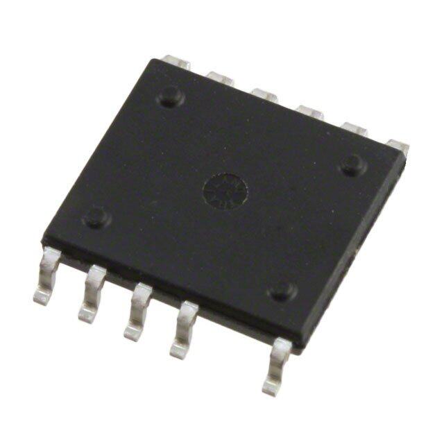
| 产品图片 |
|
| rohs | 符合RoHS无铅 / 符合限制有害物质指令(RoHS)规范要求 |
| 产品系列 | 电源管理 IC,开关控制器 ,Texas Instruments UCC2895PW- |
| 数据手册 | |
| 产品型号 | UCC2895PW |
| PWM类型 | 电流/电压模式 |
| 产品培训模块 | http://www.digikey.cn/PTM/IndividualPTM.page?site=cn&lang=zhs&ptm=9438 |
| 产品目录页面 | |
| 产品种类 | 开关控制器 |
| 倍增器 | 无 |
| 其它名称 | 296-11419-5 |
| 分频器 | 无 |
| 制造商产品页 | http://www.ti.com/general/docs/suppproductinfo.tsp?distId=10&orderablePartNumber=UCC2895PW |
| 包装 | 管件 |
| 升压 | 无 |
| 占空比 | 100% |
| 占空比-最大 | 100 % |
| 反向 | 无 |
| 反激式 | 无 |
| 商标 | Texas Instruments |
| 安装风格 | SMD/SMT |
| 封装 | Tube |
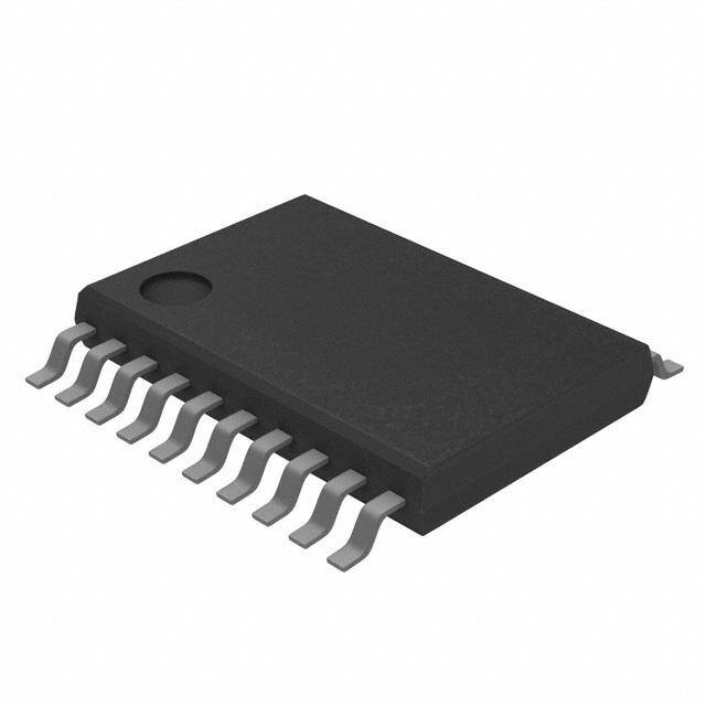
| 封装/外壳 | 20-TSSOP(0.173",4.40mm 宽) |
| 封装/箱体 | TSSOP-20 |
| 工作温度 | -40°C ~ 85°C |
| 工作电源电压 | 9 V to 16.5 V |
| 工厂包装数量 | 70 |
| 开关频率 | 1000 kHz |
| 拓扑结构 | Full-Bridge |
| 最大工作温度 | + 85 C |
| 最小工作温度 | - 40 C |
| 标准包装 | 70 |
| 电压-电源 | 10 V ~ 16.5 V |
| 类型 | BiCMOS Advanced Phase Shift Resonant Controller |
| 系列 | UCC2895 |
| 输出数 | 4 |
| 输出电流 | 100 mA |
| 输出端数量 | 4 Output |
| 降压 | 无 |
| 隔离式 | 是 |
| 频率-最大值 | 1MHz |


- 商务部:美国ITC正式对集成电路等产品启动337调查
- 曝三星4nm工艺存在良率问题 高通将骁龙8 Gen1或转产台积电
- 太阳诱电将投资9.5亿元在常州建新厂生产MLCC 预计2023年完工
- 英特尔发布欧洲新工厂建设计划 深化IDM 2.0 战略
- 台积电先进制程称霸业界 有大客户加持明年业绩稳了
- 达到5530亿美元!SIA预计今年全球半导体销售额将创下新高
- 英特尔拟将自动驾驶子公司Mobileye上市 估值或超500亿美元
- 三星加码芯片和SET,合并消费电子和移动部门,撤换高东真等 CEO
- 三星电子宣布重大人事变动 还合并消费电子和移动部门
- 海关总署:前11个月进口集成电路产品价值2.52万亿元 增长14.8%


PDF Datasheet 数据手册内容提取
Product Order Technical Tools & Support & Folder Now Documents Software Community UCC1895,UCC2895,UCC3895 SLUS157Q–DECEMBER1999–REVISEDOCTOBER2019 UCCx895 BiCMOS Advanced Phase-Shift PWM Controller 1 Features 3 Description • Programmable-outputturnondelay The UCC3895 is a phase-shift PWM controller that 1 implements control of a full-bridge power stage by • Adaptivedelayset phase shifting the switching of one half-bridge with • Bidirectionaloscillatorsynchronization respect to the other. The device allows constant • Voltage-mode,peakcurrent-mode,oraverage frequency pulse-width modulation in conjunction with current-modecontrol resonant zero-voltage switching to provide high efficiency at high frequencies. The part is used either • Programmablesoftstart,softstop,andchip asavoltage-modeorcurrent-modecontroller. disableviaasinglepin While the UCC3895 maintains the functionality of the • 0%to100%duty-cyclecontrol UC3875/6/7/8 family and UC3879, it improves on that • 7-MHzerroramplifier controller family with additional features such as • Operationto1MHz enhanced control logic, adaptive delay set, and • Typical5-mAoperatingcurrentat500kHz shutdowncapability.Because the device is built using the BCDMOS process, it operates with dramatically • Verylow150-μAcurrentduringUVLO less supply current than it’s bipolar counterparts. The UCC3895 operates with a maximum clock frequency 2 Applications of1MHz. • Phase-shiftedfull-bridgeconverters DeviceInformation(1) • Off-line,telecom,datacom,andservers PARTNUMBER PACKAGE BODYSIZE(NOM) • Distributedpowerarchitecture CDIP(20) 24.20mm×6.92mm • High-densitypowermodules LCCC(20 8.89mm×8.89mm SOIC(20) 12.80mm×7.50mm UCCx895 PDIP(20) 24.33mm×6.35mm TSSOP(20) 6.50mm×4.40mm PLCC(20) 8.96mm×8.96mm (1) For all available packages, see the orderable addendum at theendofthedatasheet. SimplifiedApplicationDiagram UCC3895 Q1 1 EAN EAP 27777777770 VOUT 2 EAOUT SS/DISB 19 3 RAMP OUTA 18 4 REF OUTB 17 A C 5 GND PGND 16 VIN 6 SYNC VDD 15 VBIAS 7 CT OUTC 14 B D 8 RT OUTD 13 9 DELAB CS 12 10 DELCD ADS 11 Copyright © 2017, Texas Instruments Incorporated 1 An IMPORTANT NOTICE at the end of this data sheet addresses availability, warranty, changes, use in safety-critical applications, intellectualpropertymattersandotherimportantdisclaimers.PRODUCTIONDATA.
UCC1895,UCC2895,UCC3895 SLUS157Q–DECEMBER1999–REVISEDOCTOBER2019 www.ti.com Table of Contents 1 Features.................................................................. 1 7.5 Programming...........................................................17 2 Applications........................................................... 1 8 ApplicationandImplementation........................ 20 3 Description............................................................. 1 8.1 ApplicationInformation............................................20 4 RevisionHistory..................................................... 2 8.2 TypicalApplication..................................................22 5 PinConfigurationandFunctions......................... 3 9 PowerSupplyRecommendations...................... 42 6 Specifications......................................................... 5 10 Layout................................................................... 42 6.1 AbsoluteMaximumRatings......................................5 10.1 LayoutGuidelines.................................................42 6.2 ESDRatings..............................................................5 10.2 LayoutExample....................................................43 6.3 RecommendedOperatingConditions.......................5 11 DeviceandDocumentationSupport................. 44 6.4 ThermalInformation..................................................6 11.1 DocumentationSupport........................................44 6.5 ElectricalCharacteristics...........................................6 11.2 ReceivingNotificationofDocumentationUpdates44 6.6 TypicalCharacteristics............................................10 11.3 CommunityResource............................................44 7 DetailedDescription............................................ 11 11.4 Trademarks...........................................................44 7.1 Overview.................................................................11 11.5 ElectrostaticDischargeCaution............................45 7.2 FunctionalBlockDiagrams.....................................11 11.6 Glossary................................................................45 7.3 FeatureDescription.................................................14 12 Mechanical,Packaging,andOrderable Information........................................................... 45 7.4 DeviceFunctionalModes........................................17 4 Revision History NOTE:Pagenumbersforpreviousrevisionsmaydifferfrompagenumbersinthecurrentversion. ChangesfromRevisionP(June2013)toRevisionQ Page • AddedESDRatingstable,FeatureDescriptionsection,DeviceFunctionalModes,ApplicationandImplementation section,PowerSupplyRecommendationssection,Layoutsection,DeviceandDocumentationSupportsection,and Mechanical,Packaging,andOrderableInformationsection.................................................................................................. 1 • ChangedUCC1895V MAX,From250mV:To300mVinElectricalCharacteristics....................................................... 8 OL • ChangedUCC1895RAMPsinkcurrentMIN,From12mA:To10mAinElectricalCharacteristics.................................... 8 • ChangedtheF noteintheDetailedDesignProceduresection ...................................................................................... 23 SW • ChangedthevoltagedropacrosstheR from0.5-Vto4.5-Vforwardvoltagedropintheoutputrectifiers..................23 DS(on) • AddedOutputVoltageSetpointsection................................................................................................................................ 34 • AddedSettingtheSwitchingFrequencysection.................................................................................................................. 36 • AddedSoftStartsection....................................................................................................................................................... 36 • AddedSettingtheSwitchingDelayssection........................................................................................................................ 36 • AddedSettingtheSlopeCompensationsection.................................................................................................................. 38 ChangesfromRevisionO(April2010)toRevisionP Page • AddedTheCSinputconnectstotexttothebeginningoftheCSDetailedPinDescription................................................ 14 • AddedsecondparagraphtodetailedREFPinDescriptionandincludedtheUCC1895attheendofthefirst paragraphtodifferentiatecapacitancecapabilitiesofthedevices....................................................................................... 16 • ChangedUCC3895TimingDiagramintheApplicationInformationsectiontoreflectthemaximumdutycycleconditions19 ChangesfromRevisionN(May2009)toRevisionO Page • ChangedREFpindescriptionfrom“Donotusemorethan1.0μFoftotalcapacitanceonthispin.”to“Donotuse morethan4.7μFoftotalcapacitanceonthispin.”.............................................................................................................. 16 2 SubmitDocumentationFeedback Copyright©1999–2019,TexasInstrumentsIncorporated ProductFolderLinks:UCC1895 UCC2895 UCC3895
UCC1895,UCC2895,UCC3895 www.ti.com SLUS157Q–DECEMBER1999–REVISEDOCTOBER2019 5 Pin Configuration and Functions PWANDDWPACKAGEDRAWINGS (TOPVIEW) NANDJPACKAGEDRAWINGS (TOPVIEW) PWandDWPACKAGE (TOPVIEW) EAN 1 20 EAP EAN 1 20 EAP EAOUT 2 19 SS/DISB EAOUT 2 19 SS/DISB RAMP 3 18 OUTA RAMP 3 18 OUTA REF 4 17 OUTB REF 4 17 OUTB GND 5 16 PGND GND 5 16 PGND SYNC 6 15 VDD SYNC 6 15 VDD CT 7 14 OUTC CT 7 14 OUTC RT 8 13 OUTD DELAB 9 12 CS RT 8 13 OUTD DELCD 10 11 ADS DELAB 9 12 CS DELCD 10 11 ADS FNANDFKPACKAGEDRAWINGS (TOPVIEW) EAN EAOUT EAP RAMP SS/DISB 3 2 1 20 19 REF 4 18 OUTA GND 5 17 OUTB SYNC 6 16 PGND CT 7 15 VDD RT 8 14 OUTC 9 10 11 12 13 DELAB OUTD DELCD CS ADS Copyright©1999–2019,TexasInstrumentsIncorporated SubmitDocumentationFeedback 3 ProductFolderLinks:UCC1895 UCC2895 UCC3895
UCC1895,UCC2895,UCC3895 SLUS157Q–DECEMBER1999–REVISEDOCTOBER2019 www.ti.com PinFunctions PIN I/O DESCRIPTION NAME NO. Theadaptive-delay-setpinsetstheratiobetweenthemaximumandminimumprogrammedoutputdelay ADS 11 I deadtime. CS 12 I Currentsenseinputforcycle-by-cyclecurrentlimitingandforover-currentcomparator. Oscillatortimingcapacitorforprogrammingtheswitchingfrequency.TheUCC3895oscillatorchargesCTvia CT 7 I aprogrammedcurrent. Thedelay-programmingbetweencomplementary-outputspin,DELAB,programsthedeadtimebetween DELAB 9 I switchingofoutputAandoutputB. Thedelay-programmingbetweencomplementary-outputspin,DELCD,programsthedeadtimebetween DELCD 10 I switchingofoutputCandoutputD. EAOUT 2 I/O Erroramplifieroutput. EAP 20 I Non-invertinginputtotheerroramplifier.Keepbelow3.6Vforproperoperation. EAN 1 I Invertinginputtotheerroramplifier.Keepbelow3.6Vforproperoperation. GND 5 — Chipgroundforallcircuitsexcepttheoutputstages. OUTA 18 O OUTB 17 O Thefouroutputsare100-mAcomplementaryMOSdrivers,andareoptimizedtodriveFETdrivercircuits OUTC 14 O suchasUCC27714orgatedrivetransformers. OUTD 13 O PGND 16 — Outputstageground. RAMP 3 I InvertinginputofthePWMcomparator. 5-V,±1.2%,5-mAvoltagereference.Forbestperformance,bypasswitha0.1-μFlowESR,lowESL REF 4 O capacitortoground.Donotusemorethan4.7μFoftotalcapacitanceonthispin. RT 8 I Oscillatortimingresistorforprogrammingtheswitchingfrequency. SS/DISB 19 I Soft-startanddisablepinwhichcombinesthetwoindependentfunctions. SYNC 6 I/O Theoscillatorsynchronizationpinisbidirectional. Thepowersupplyinputpin,VDD,mustbebypassedwithaminimumofa1-μFlowESR,lowESLcapacitor VDD 15 I toground.Theadditionofa10-μFlowESR,lowESLbetweenVDDandPGNDisrecommended. 4 SubmitDocumentationFeedback Copyright©1999–2019,TexasInstrumentsIncorporated ProductFolderLinks:UCC1895 UCC2895 UCC3895
UCC1895,UCC2895,UCC3895 www.ti.com SLUS157Q–DECEMBER1999–REVISEDOCTOBER2019 6 Specifications 6.1 Absolute Maximum Ratings overoperatingfree-airtemperaturerange(unlessotherwisenoted)(1) MIN MAX UNIT Supplyvoltage 17 V Outputcurrent 100 mA Referencecurrent 15 mA Supplycurrent 30 mA EAP,EAN,EAOUT,RAMP,SYNC,ADS,CS, Analoginputs –0.3 REF+0.3 V SS/DISB Driveoutputs OUTA,OUTB,OUTC,OUTD –0.3 VCC+0.3 V DW-20package 650 mW PowerdissipationatT =25°C A N-20package 1 W T Junctiontemperature –55 150 °C J T Storagetemperature –65 150 °C stg (1) StressesbeyondthoselistedunderAbsoluteMaximumRatingsmaycausepermanentdamagetothedevice.Thesearestressratings only,whichdonotimplyfunctionaloperationofthedeviceattheseoranyotherconditionsbeyondthoseindicatedunderRecommended OperatingConditions.Exposuretoabsolute-maximum-ratedconditionsforextendedperiodsmayaffectdevicereliability. 6.2 ESD Ratings VALUE UNIT Human-bodymodel(HBM),perANSI/ESDA/JEDECJS-001(1) ±1000 V Electrostaticdischarge V (ESD) Charged-devicemodel(CDM),perJEDECspecificationJESD22-C101(2) ±1000 (1) JEDECdocumentJEP155statesthat500-VHBMallowssafemanufacturingwithastandardESDcontrolprocess. (2) JEDECdocumentJEP157statesthat250-VCDMallowssafemanufacturingwithastandardESDcontrolprocess. 6.3 Recommended Operating Conditions overoperatingfree-airtemperaturerange(unlessotherwisenoted)(1) MIN NOM MAX UNIT V Supplyvoltage 10 16.5 V DD V Supplyvoltagebypasscapacitor(2) 10×C µF DD REF C Referencebypasscapacitor(UCC1895)(3) 0.1 1 µF REF C Referencebypasscapacitor(UCC2895,UCC3895)(3) 0.1 4.7 µF REF C Timingcapacitor(for500-kHzswitchingfrequency) 220 pF T R Timingresistor(for500-kHzswitchingfrequency) 82 kΩ T R ,R Delayresistor 2.5 40 kΩ DEL_AB DEL_CD T Operatingjunctiontemperature(4) –55 125 °C J (1) TIrecommendsthattherebeasinglepointgroundedbetweenGNDandPGNDdirectlyunderthedevice.Theremustbeaseparate groundplaneassociatedwiththeGNDpinandallcomponentsassociatedwithpins1through12,plus19and20,belocatedoverthis groundplane.Anyconnectionsassociatedwiththesepinstogroundmustbeconnectedtothisgroundplane. (2) TheV capacitormustbealowESR,ESLceramiccapacitorlocateddirectlyacrosstheVDDandPGNDpins.Alargerbulkcapacitor DD mustbelocatedasphysicallycloseaspossibletotheV pins. DD (3) TheV capacitormustbealowESR,ESLceramiccapacitorlocateddirectlyacrosstheREFandGNDpins.Ifalargercapacitoris REF desiredfortheV thenitmustbelocatedneartheV capandconnectedtotheV pinwitharesistorof51Ωorgreater.Thebulk REF REF REF capacitoronV mustbeafactorof10greaterthanthetotalV capacitance. DD REF (4) TIdoesnotrecommendedthatthedeviceoperateunderconditionsbeyondthosespecifiedinthistableforextendedperiodsoftime. Copyright©1999–2019,TexasInstrumentsIncorporated SubmitDocumentationFeedback 5 ProductFolderLinks:UCC1895 UCC2895 UCC3895
UCC1895,UCC2895,UCC3895 SLUS157Q–DECEMBER1999–REVISEDOCTOBER2019 www.ti.com 6.4 Thermal Information UCC2895 UCC2895 UCC1895 UCC3895 UCC3895 UCC3895 THERMALMETRIC(1) J FK DW PW FN N UNIT (CDIP) (LCCC) (SOIC) (TSSOP) (PLCC) (PDIP) 20PINS 20PINS 20PINS 20PINS 20PINS 20PINS R Junction-to-ambientthermalresistance N/A N/A 66.4 91.0 54.8 48.6 °C/W θJA Junction-to-case(top)thermal R 34.2 31.2 31.6 26.1 32.8 35.6 °C/W θJC(top) resistance R Junction-to-boardthermalresistance 48.9 30.9 34.1 42.2 19.0 29.6 °C/W θJB Junction-to-topcharacterization ψ N/A N/A 8.6 1.3 9.0 16.0 °C/W JT parameter Junction-to-boardcharacterization ψ N/A N/A 33.7 41.6 18.7 29.4 °C/W JB parameter Junction-to-case(bottom)thermal R 8.9 3.3 N/A N/A N/A N/A °C/W θJC(bot) resistance (1) Formoreinformationabouttraditionalandnewthermalmetrics,seetheSemiconductorandICPackageThermalMetricsapplication report,SPRA953. 6.5 Electrical Characteristics V =12V,R =82kΩ,C =220pF,R =10kΩ,R =10kΩ,C =0.1μF,C =0.1μFandnoloadonthe DD T T DELAB DELCD REF VDD outputs,T =T.T =0°Cto70°CforUCC3895x,T =–40°Cto85°CforUCC2895xandT =–55°Cto125°Cforthe A J A A A UCC1895x(unlessotherwisenoted) PARAMETER TESTCONDITIONS MIN TYP MAX UNIT UVLO(UNDERVOLTAGELOCKOUT) UVLO Start-upvoltagethreshold 10.2 11 11.8 V (on) UVLO Minimumoperatingvoltageafterstart-up 8.2 9 9.8 V (off) UVLO Hysteresis 1 2 3 V (hys) SUPPLY I Start-upcurrent VDD=8V 150 250 µA START I Operatingcurrent 5 6 mA DD V V clampvoltage IDD=10mA 16.5 17.5 18.5 V DD_CLAMP DD VOLTAGEREFERENCE T =25°C 4.94 5 5.06 J VREF Outputvoltage 10V<VDD<VDD_CLAMP, V 0mA<IREF<5mA, 4.85 5 5.15 temperature I Shortcircuitcurrent REF=0V,T =25°C 10 20 mA SC J ERRORAMPLIFIER Common-modeinputvoltagerange –0.1 3.6 V V Offsetvoltage –7 7 mV IO I Inputbiascurrent(EAP,EAN) –1 1 µA BIAS EAOUT High-leveloutputvoltage EAP–EAN=500mV,I =–0.5mA 4 4.5 5 V _VOH EAOUT EAOUT Low-leveloutputvoltage EAP–EAN=–500mV,I =0.5mA 0 0.2 0.4 V _VOL EAOUT I Erroramplifieroutputsourcecurrent EAP–EAN=500mV,EAOUT=2.5V 1 1.5 mA SOURCE I Erroramplifieroutputsinkcurrent EAP–EAN=–500mV,EAOUT=2.5V 2.5 4.5 mA SINK A Open-loopdcgain 75 85 dB VOL GBW Unitygainbandwidth(1) 5 7 mHz Slewrate(1) 1V<EAN<0V,EAP=500mV, 1.5 2.2 V/µs 0.5V<EAOUT<3V No-loadcomparatorturn-offthreshold 0.45 0.5 0.55 V No-loadcomparatorturn-onthreshold 0.55 0.6 0.69 V (1) Ensuredbydesign.Notproductiontested. 6 SubmitDocumentationFeedback Copyright©1999–2019,TexasInstrumentsIncorporated ProductFolderLinks:UCC1895 UCC2895 UCC3895
UCC1895,UCC2895,UCC3895 www.ti.com SLUS157Q–DECEMBER1999–REVISEDOCTOBER2019 Electrical Characteristics (continued) V =12V,R =82kΩ,C =220pF,R =10kΩ,R =10kΩ,C =0.1μF,C =0.1μFandnoloadonthe DD T T DELAB DELCD REF VDD outputs,T =T.T =0°Cto70°CforUCC3895x,T =–40°Cto85°CforUCC2895xandT =–55°Cto125°Cforthe A J A A A UCC1895x(unlessotherwisenoted) PARAMETER TESTCONDITIONS MIN TYP MAX UNIT No-loadcomparatorhysteresis 0.035 0.1 0.165 V OSCILLATOR f Frequency T =25°C 473 500 527 kHz OSC J Frequencytotalvariation Overline,temperature 2.5% 5% V SYNCinputthreshold,SYNC 2.05 2.1 2.4 V IH_SYNC V High-leveloutputvoltage,SYNC I =–400μA,V =2.6V 4.1 4.5 5 V OH_SYNC SYNC CT V Low-leveloutputvoltage,SYNC I =100μA,V =0V 0 0.5 1 V OL_SYNC SYNC CT Syncoutputpulsewidth LOAD =3.9kΩand30pFinparallel 85 135 ns SYNC V Timingresistorvoltage 2.9 3 3.1 V RT V Timingcapacitorpeakvoltage 2.25 2.35 2.55 V CT(peak) V Timingcapacitorvalleyvoltage 0 0.2 0.4 V CT(valley) CURRENTSENSE 0V<CS<2.5V, I Currentsensebiascurrent –4.5 20 µA CS(bias) 0VADS<2.5V Peakcurrentthreshold 1.9 2 2.1 V Overcurrentthreshold 2.4 2.5 2.6 V 0V≤CS≤2.3V, Currentsensetooutputdelay 75 110 ns DELAB=DELCD=REF SOFTSTART/SHUTDOWN SS/DISB=3.0V, I Soft-startsourcecurrent –40 –35 –30 µA SOURCE CS=1.9V SS/DISB=3.0V, I Soft-startsinkcurrent 325 350 375 µA SINK CS=2.6V Soft-start/disablecomparatorthreshold 0.44 0.5 0.56 V ADAPTIVEDELAYSET(ADS) ADS=CS=0V 0.45 0.5 0.55 DELAB/DELCDoutputvoltage ADS=0V, V 1.9 2 2.1 CS=2V t Outputdelay(1)(2) ADS=CS=0V 450 560 620 ns DELAY 0V<ADS<2.5V, ADSbiascurrent –20 20 µA 0V<CS<2.5V (2) OutputdelayismeasuredbetweenOUTAandOUTB,orOUTCandOUTD.Outputdelayisdefinedasshownbelowwhere:t = f(OUTA) fallingedgeofOUTAsignal,t =risingedgeofOUTBsignal(seeFigure1andFigure2). r(OUTB) Copyright©1999–2019,TexasInstrumentsIncorporated SubmitDocumentationFeedback 7 ProductFolderLinks:UCC1895 UCC2895 UCC3895
UCC1895,UCC2895,UCC3895 SLUS157Q–DECEMBER1999–REVISEDOCTOBER2019 www.ti.com Electrical Characteristics (continued) V =12V,R =82kΩ,C =220pF,R =10kΩ,R =10kΩ,C =0.1μF,C =0.1μFandnoloadonthe DD T T DELAB DELCD REF VDD outputs,T =T.T =0°Cto70°CforUCC3895x,T =–40°Cto85°CforUCC2895xandT =–55°Cto125°Cforthe A J A A A UCC1895x(unlessotherwisenoted) PARAMETER TESTCONDITIONS MIN TYP MAX UNIT OUTPUT V High-leveloutputvoltage(alloutputs) I =–10mA,VDDtooutput 250 400 mV OH OUT UCC1895 150 300 V Low-leveloutputvoltage(alloutputs) I =10mA mV OL OUT UCC2895,UCC3895 150 250 t Risetime(1) C =100pF 20 35 ns R LOAD t Falltime(1) C =100pF 20 35 ns F LOAD PWMCOMPARATOR RAMP=0V, EAOUTtoRAMPinputoffsetvoltage 0.72 0.85 1.05 V DELAB=DELCD=REF Minimumphaseshift(3) RAMP=0V, 0.0% 0.85% 1.4% (OUTAtoOUTC,OUTBtoOUTD) EAOUT=650mV Delay(2) 0V<RAMP<2.5V,EAOUT=1.2V, t 70 120 ns DELAY (RAMPtoOUTC,RAMPtoOUTD) DELAB=DELCD=REF I RAMPbiascurrent RAMP<5V,CT=2.2V –5 5 µA R(bias) RAMP=5V, UCC1895 10 19 I RAMPsinkcurrent mA R(sink) CT=2.6V UCC2895,UCC3895 12 19 (3) Minimumphaseshiftisdefinedas: t -t t -t f(OUTC) f(OUTA) f(OUTC) f(OUTB) F =180´ or F =180´ t t PERIOD PERIOD where (a)t =fallingedgeofOUTAsignal f(OUTA) (b)t =fallingedgeofOUTBsignal f(OUTB) (c)t =fallingedgeofOUTCsignal f(OUTC) (d)t =fallingedgeofOUTDsignal f(OUTD) (e)t =periodofOUTAorOUTBsignal PERIOD t PERIOD OUTA t = t - t DELAY f(OUTA) f(OUTC) OUTC Figure1. SameAppliestoOUTBandOUTD 8 SubmitDocumentationFeedback Copyright©1999–2019,TexasInstrumentsIncorporated ProductFolderLinks:UCC1895 UCC2895 UCC3895
UCC1895,UCC2895,UCC3895 www.ti.com SLUS157Q–DECEMBER1999–REVISEDOCTOBER2019 OUTA t = t - t DELAY R(OUTB) f(OUTA) OUTB Figure2. SameAppliestoOUTCandOUTD Copyright©1999–2019,TexasInstrumentsIncorporated SubmitDocumentationFeedback 9 ProductFolderLinks:UCC1895 UCC2895 UCC3895
UCC1895,UCC2895,UCC3895 SLUS157Q–DECEMBER1999–REVISEDOCTOBER2019 www.ti.com 6.6 Typical Characteristics 2000 1600 Vcs = 0 V RT = 47 k(cid:13) 1800 1400 RT = 62 k(cid:13) 1600 Vcs = 2 V Hz) 1200 RRTT == 8120 0k (cid:13)k(cid:13) Delay (ns) 111024000000 equency (k1080000 Output 680000 cillator Fr 460000 400 Os 200 200 0 0 0 10 20 30 40 100 1000 Delay Resistance (k(cid:13)(cid:12) C001 Timing Capacitance (pF) C002 Figure3.OutputDelay(tDELAY)vs Figure4.OscillatorFrequency(fSW)vs DelayResistance(RDEL) TimingCapacitance(CT) 1.00 100 200 V) 80 160 et (0.95 p Offs dB) 60 120 °gin() Ram0.90 ain( Mar o G 40 80 se T t ha U P O0.85 A 20 40 E Gain (dB) Phase Margin(°C) 0.80 0 0 –60 –40 –20 0 20 40 60 80 100 120 1 10 100 1k 10k 100k 1M 10M Temperature ((cid:131)C) C003 Frequency(Hz) C004 Figure5.EAOUTtoRampOffset(VOFFSET)vs Figure6.AmplifierGainandPhaseMarginvs Temperature(TA) Frequency(fOSC) 9 13 Vdd = 10 V Vdd = 10 V Vdd = 12 V 12 Vdd = 12 V Vdd = 15 V Vdd = 15 V 8 Vdd = 17 V 11 Vdd = 17 V 10 A) 7 A) 9 m m d ( d ( 8 Id6 Id 7 5 6 5 4 4 0 400 800 1200 1600 0 400 800 1200 1600 Oscillator Frequency (kHz) C005 Oscillator Frequency (kHz) C006 Figure7.InputCurrent(IDD)vs Figure8.InputCurrent(IDD)vs OscillatorFrequency(fOSC) OscillatorFrequency(fOSC) 10 SubmitDocumentationFeedback Copyright©1999–2019,TexasInstrumentsIncorporated ProductFolderLinks:UCC1895 UCC2895 UCC3895
UCC1895,UCC2895,UCC3895 www.ti.com SLUS157Q–DECEMBER1999–REVISEDOCTOBER2019 7 Detailed Description 7.1 Overview TheUCC3895devicecombinesallthefunctions necessary to control a phase-shifted full bridge power stage in a 20-pin package. It includes all the outputs needed to drive the four switches in the full-bridge circuit. The dead times between the upper and lower switches in the full bridge may be set using the DELAB and DELCD inputs. Further, this dead time may be dynamically adjusted according to the load level using the ADS pin allowing the user to optimize the dead time for their particular power circuit and to achieve ZVS over the entire operating range. At light loads a no-load comparator forces cycle skipping to maintain output voltage regulation. At higher- power levels, two or more UCC3895 devices may be easily synchronized for parallel operation. The SS/DISB input may be used to set the length of the soft-start process and to turn the controller on and off. The controller may be used in Voltage mode or Current mode control and cycle-by-cycle current limiting is provided in both modes. The switching frequency may be set over a wide range making this device suited to both IGBT and MOSFETbaseddesigns. 7.2 Functional Block Diagrams + VOUT VIN CIN UCC3895 - 1 EAN EAP 20 2 EAOUT SS/DISB 19 3 RAMP OUTA 18 A QA QC 4 REF OUTB 17 B A DB C T1 5 GND PGND 16 LS 6 SYNC VDD 15 DC QB QD 7 CT OUTC 14 C B D 8 RT OUTD 13 D 9 DELAB CS 12 VOUT 10 DELCD ADS 11 + - Copyright © 2017, Texas Instruments Incorporated Figure9. SimplifiedApplicationDiagram Copyright©1999–2019,TexasInstrumentsIncorporated SubmitDocumentationFeedback 11 ProductFolderLinks:UCC1895 UCC2895 UCC3895
UCC1895,UCC2895,UCC3895 SLUS157Q–DECEMBER1999–REVISEDOCTOBER2019 www.ti.com Functional Block Diagrams (continued) IRT RT 8 Q 15 VDD D S Q 8(IRT) OSC CT 7 Q OUTA D S Q DELAY A 18 Q R 9 DELAB SYNC 6 PWM R Q DELAY B 17 OUTB COMPARATOR RAMP 3 + 0.8 V + EAOUT 2 14 OUTC ERROR D S Q DELAY C EAP 20 AMP CONMOP ALORAATDO R 10 DELCD + + R Q DELAY D EAN 1 13 OUTD CURRENT SENSE COMPARATOR 0.5 V / 0.6 V 2 V + 16 PGND CS 12 11 ADS OVER CURRENT ADAPTIVE DELAY SET COMPARATOR + AMPLIFIER 2.5 V + 0.5V Q S UVLO COMPARATOR + REF Q R 11 V / 9 V DISABLE IRT COMPARATOR REF 4 REF HI=ON 0.5 V REFERENCE OK SS 19 + COMPARATOR HI=ON 4 V 5 GND + 10(I ) RT Copyright © 2017, Texas Instruments Incorporated Figure10. BlockDiagram 12 SubmitDocumentationFeedback Copyright©1999–2019,TexasInstrumentsIncorporated ProductFolderLinks:UCC1895 UCC2895 UCC3895
UCC1895,UCC2895,UCC3895 www.ti.com SLUS157Q–DECEMBER1999–REVISEDOCTOBER2019 Functional Block Diagrams (continued) REF VREF RT 8IRT RT IRT CT 2.5 V S Q CLOCK + CT 0.2 V + R SYNC CLOCK Figure11. OscillatorBlockDiagram REF 0.5 V TO DELAY A 100 k: 75 k: + AND DELAY B BLOCKS CS DELAB + 100 k: ADS 75 k: REF TO DELAY C + AND DELAY D DELCD BLOCKS Figure12. AdaptiveDelaySetBlockDiagram Copyright©1999–2019,TexasInstrumentsIncorporated SubmitDocumentationFeedback 13 ProductFolderLinks:UCC1895 UCC2895 UCC3895
UCC1895,UCC2895,UCC3895 SLUS157Q–DECEMBER1999–REVISEDOCTOBER2019 www.ti.com Functional Block Diagrams (continued) REF BUSSED CURRENT FROM ADS CIRCUIT 3.5 V DELAB/CD FROM PAD DELAYED 2.5 V CLOCK SIGNAL CLOCK Figure13. DelayBlockDiagram(OneDelayBlockPerOutlet) 7.3 Feature Description 7.3.1 ADS(AdaptiveDelaySet) This function sets the ratio between the maximum and minimum programmed output-delay dead time. When the ADS pin is directly connected to the CS pin, no delay modulation occurs. The maximum delay modulation occurs whenADSisgrounded.Inthiscase,delaytimeis four-times longer when CS = 0 than when CS = 2 V (the peak- currentthreshold),ADSchangestheoutputvoltageonthedelaypinsDELABandDELCDbyEquation1. V = é0.75´(V -V )ù+0.5 V DEL ë CS ADS û where • V andV areinvolts (1) CS ADS ADS must be limited to between 0 V and 2.5 V and must be less-than or equal-to CS. DELAB and DELCD are clampedtoaminimumof0.5V. 7.3.2 CS(CurrentSense) The CS input connects to the inverting input of the current-sense comparator and the non-inverting input of the overcurrent comparator and the ADS amplifier. The current sense signal is used for cycle-by-cycle current limiting in peak current-mode control, and for overcurrent protection in all cases with a secondary threshold for outputshutdown.Anoutputdisableinitiatedbyanovercurrentfaultalsoresultsinarestartcycle, called soft stop, withfullsoftstart. 7.3.3 CT(OscillatorTimingCapacitor) The UCC3895 oscillator charges CT via a programmed current. The waveform on C is a sawtooth, with a peak T voltageof2.35V.TheapproximateoscillatorperiodiscalculatedbyEquation2. 5´R ´C t = T T +120ns OSC 48 where • C isinFarads T • R isinOhms T • t isinseconds OSC • C canrangefrom100to880pF (2) T 14 SubmitDocumentationFeedback Copyright©1999–2019,TexasInstrumentsIncorporated ProductFolderLinks:UCC1895 UCC2895 UCC3895
UCC1895,UCC2895,UCC3895 www.ti.com SLUS157Q–DECEMBER1999–REVISEDOCTOBER2019 Feature Description (continued) NOTE A large C and a small R combination results in extended fall times on the C waveform. T T T The increased fall time increases the SYNC pulse width, hence limiting the maximum phase shift between OUTA, OUTB and OUTC, OUTD outputs, which limits the maximum dutycycleoftheconverter(seeFigure11). 7.3.4 DELABandDELCD(DelayProgrammingBetweenComplementaryOutputs) DELAB programs the dead time between switching of OUTA and OUTB. DELCD programs the dead time between OUTC and OUTD. This delay is introduced between complementary outputs in the same leg of the externalbridge.TheUCC3895allows the user to select the delay, in which the resonant switching of the external power stages takes place. Separate delays are provided for the two half-bridges to accommodate differences in resonant-capacitorchargingcurrents.ThedelayineachstageissetaccordingtoEquation3. (25´10-12)´R DEL t = +25ns DELAY V DEL where • V isinvolts DEL • R isinOhms DEL • t isinseconds (3) DELAY DELAB and DELCD source about 1-mA maximum. Choose the delay resistors so that this maximum is not exceeded. Programmable output delay is defeated by tying DELAB and, or, DELCD to REF. For an optimum performancekeepstraycapacitanceonthesepinsatlessthan10pF. 7.3.5 EAOUT,EAP,andEAN(ErrorAmplifier) EAOUT connects internally to the non-inverting input of the PWM comparator and the no-load comparator. EAOUT is internally clamped to the soft-start voltage. The no-load comparator shuts down the output stages whenEAOUTfallsbelow500mV,andallowstheoutputstoturnonagainwhenEAOUTrisesabove600mV. EAPisthenon-invertingandtheEANistheinvertinginputtotheerroramplifier. 7.3.6 OUTA,OUTB,OUTC,andOUTD(OutputMOSFETDrivers) The four outputs are 100-mA complementary MOS drivers, and are optimized to drive MOSFET driver circuits. OUTA and OUTB are fully complementary, (assuming no programming delay) and operate near 50% duty cycle andone-halftheoscillatorfrequency.OUTAandOUTBareintendedtodriveone half-bridge circuit in an external power stage. OUTC and OUTD drive the other half-bridge and have the same characteristics as OUTA and OUTB.OUTCisphaseshiftedwithrespecttoOUTA,andOUTDisphaseshiftedwithrespecttoOUTB. NOTE Changing the phase relationship of OUTC and OUTD with respect to OUTA and OUTB requires other than the nominal 50% duty ratio on OUTC and OUTD during those transients. 7.3.7 PGND(PowerGround) To keep output switching noise from critical analog circuits, the UCC3895 has two different ground connections. PGNDisthegroundconnectionforthehigh-currentoutputstages.BothGND and PGND must be electrically tied together.Also,becausePGNDcarrieshighcurrent,boardtracesmustbelowimpedance. 7.3.8 RAMP(InvertingInputofthePWMComparator) This pin receives either the C waveform in voltage and average current-mode controls, or the current signal T (plusslopecompensation)inpeakcurrent-modecontrol. Copyright©1999–2019,TexasInstrumentsIncorporated SubmitDocumentationFeedback 15 ProductFolderLinks:UCC1895 UCC2895 UCC3895
UCC1895,UCC2895,UCC3895 SLUS157Q–DECEMBER1999–REVISEDOCTOBER2019 www.ti.com Feature Description (continued) 7.3.9 REF(VoltageReference) The 5-V ± 1.2% reference supplies power to internal circuitry, and also supplies up to 5 mA to external loads. The reference is shutdown during undervoltage lockout but is operational during all other disable modes. For best performance, bypass with a 0.1-μF low-ESR low-ESL capacitor to GND. To ensure the stability of the internalreference,donotusemorethan1μFoftotalcapacitanceonthispinfortheUCC1895. For the UCC2895 and the UCC3895, this capacitance increases as per the limits defined in the Recommended OperatingConditionsofthisspecification. 7.3.10 RT(OscillatorTimingResistor) The oscillator in the UCC3895 operates by charging an external timing capacitor, C , with a fixed current T programmedbyR .R currentiscalculatedwithEquation4. T T 3 V I (A)= RT R (W) T (4) R rangesfrom40kΩ to 120 kΩ. Soft-start charging and discharging currents are also programmed by I (Refer T RT toFigure11). 7.3.11 GND(AnalogGround) Thispinisthechipgroundforallinternalcircuitsexcepttheoutputstages. 7.3.12 SS/DISB(SoftStart/Disable) Thispincombinestwoindependentfunctions. Disable Mode: A rapid shutdown of the chip is accomplished by externally forcing SS/DISB below 0.5 V, externally forcing REF below 4 V, or if VDD drops below the undervoltage lockout threshold. In the case of REF being pulled below 4 V or an undervoltage condition, SS/DISB is actively pulled to ground via an internal MOSFETswitch. If an overcurrent fault is sensed (CS = 2.5 V), a soft stop is initiated. In this mode, SS/DISB sinks a constant current of (10 × I ). The soft stop continues until SS/DISB falls below 0.5 V. When any of these faults are RT detected,alloutputsareforcedtogroundimmediately. NOTE If SS/DISB is forced below 0.5 V, the pin starts to source current equal to I . The only RT time the part switches into low I current mode, though, is when the part is in DD undervoltagelockout. Soft Start Mode: After a fault or disable condition has passed, VDD is above the start threshold, and, or, SS/DISB falls below 0.5 V during a soft stop, SS/DISB switches to a soft-start mode. The pin then sources current, equal to I . A user-selected resistor/capacitor combination on SS/DISB determines the soft-start time RT constant. NOTE SS/DISB actively clamps the EAOUT pin voltage to approximately the SS/DISB pin voltageduringsoft-start,soft-stop,anddisableconditions. 16 SubmitDocumentationFeedback Copyright©1999–2019,TexasInstrumentsIncorporated ProductFolderLinks:UCC1895 UCC2895 UCC3895
UCC1895,UCC2895,UCC3895 www.ti.com SLUS157Q–DECEMBER1999–REVISEDOCTOBER2019 Feature Description (continued) 7.3.13 SYNC(OscillatorSynchronization) This pin is bidirectional (refer to Figure 11). When used as an output, SYNC is used as a clock, which is the same as the internal clock of the device. When used as an input, SYNC overrides the internal oscillator of the chip and acts as the clock signal. This bidirectional feature allows synchronization of multiple power supplies. Also, the SYNC signal internally discharge the C capacitor and any filter capacitors that are present on the T RAMP pin. The internal SYNC circuitry is level sensitive, with an input-low threshold of 1.9 V, and an input-high threshold of 2.1 V. A resistor as small as 3.9 kΩ may be tied between SYNC and GND to reduce the sync pulse width. 7.3.14 VDD(ChipSupply) This is the input pin to the chip. VDD must be bypassed with a minimum of 1-μF low ESR, low ESL capacitor to ground.Theadditionofa10-μFlowESR,lowESLbetweenVDDandPGNDisrecommended. 7.4 Device Functional Modes The UCC3895 has a number of operational modes. These modes are described in detail in Feature Description section. • Current mode - The UCC3895 device may be operated in current mode control. The CS pin is connected to thecurrentsensesignalplusslopecompensation.TheRAMPpinisconnectedtotheCSpin. • Voltage mode - The UCC3895 may be operated in voltage mode control. The RAMP pin is connected to the signalatCT. • Light load mode - Under light load conditions the signal at the EAOUT pin can fall below the threshold of the No-Load-Comparator.WhenthishappenstheUCC3895maintainsoutputregulationbyskippingcycles. • Synchronized mode - Multiple UC3895 devices may be synchronised to each other or to an external clock signal. • Disablemode-ThedevicewillstopiftheEN/DISBpinispulledbelow0.5V. • Soft-startmode-Thismodeprotectsthepowerstagefromexcessivestressesduringthestart-upprocess. 7.5 Programming 7.5.1 ProgrammingDELAB,DELCDandtheAdaptiveDelaySet The UCC3895 allows the user to set the delay between switch commands within each leg of the full-bridge powercircuitaccordingtoEquation5. (25´10-12)´R DEL t = +25ns DELAY V DEL (5) From Equation 5 VDEL is determined in conjunction with the desire to use (or not) the ADS feature from Equation6. V = é0.75´(V -V )ù+0.5 V DEL ë CS ADS û (6) Figure14illustratestheresistorsneededtoprogramthedelayperiodsandtheADSfunction. Copyright©1999–2019,TexasInstrumentsIncorporated SubmitDocumentationFeedback 17 ProductFolderLinks:UCC1895 UCC2895 UCC3895
UCC1895,UCC2895,UCC3895 SLUS157Q–DECEMBER1999–REVISEDOCTOBER2019 www.ti.com Programming (continued) UCC3895 CS 12 9 DELAB R DELAB 10 DELCD ADS 11 R DELCD Figure14. ProgrammingAdaptiveDelaySet The ADS allows the user to vary the delay times between switch commands within each of the two legs of the converter. The delay-time modulation is implemented by connecting ADS (pin 11) to CS, GND, or a resistive divider from CS through ADS to GND to set V as shown in Figure 14. From Equation 6 for V , if ADS is tied ADS DEL to GND then V rises in direct proportion to V , causing a decrease in t as the load increases. In this DEL CS DELAY condition,themaximumvalueofV is2V. DEL If ADS is connected to a resistive divider between CS and GND, the term (V – V ) becomes smaller, CS ADS reducing the level of V . This reduction decreases the amount of delay modulation. In the limit of ADS tied to DEL CS, V = 0.5 V and no delay modulation occurs. Figure 15 graphically shows the delay time versus load for DEL varyingadaptivedelaysetfeaturevoltages(V ). ADS In the case of maximum delay modulation (ADS = GND), when the circuit goes from light load to heavy load, the variation of V is from 0.5 to 2 V. This change causes the delay times to vary by a 4:1 ratio as the load is DEL changed. The ability to program an adaptive delay is a desirable feature because the optimum delay time is a function of the current flowing in the primary winding of the transformer, and changes by a factor of 10:1 or more as circuit loading changes. Reference 7 (see the Related Documentation section) describes the many interrelated factors forchoosingtheoptimumdelaytimesfor the most efficient power conversion, and illustrates an external circuit to enable ADS using the UC3879. Implementing this adaptive feature is simplified in the UCC3895 controller, giving theusertheabilitytotailorthedelaytimestosuitaparticularapplicationwithaminimumofexternalparts. 18 SubmitDocumentationFeedback Copyright©1999–2019,TexasInstrumentsIncorporated ProductFolderLinks:UCC1895 UCC2895 UCC3895
UCC1895,UCC2895,UCC3895 www.ti.com SLUS157Q–DECEMBER1999–REVISEDOCTOBER2019 Programming (continued) DELAY TIME vs CURRENT SENSE VOLTAGE A = V /V R = 10k(cid:13) ADS CS DELAY 500 A=1.0 ) s n ( 400 E M I T A=0.8 Y 300 A L E A=0.6 D 200 A=0.4 A=0.2 A=0.1 100 0 0.5 1.0 1.5 2.0 2.5 CURRENT SENSE VOLTAGE (V) Figure15. DelayTimeUnderVaryingADSVoltages CLOCK RAMP & COMP PWM SIGNAL OUTPUT A OUTPUT B OUTPUT C OUTPUT D NoOutputDelayShown,COMPtoRAMPoffsetnotincluded. Figure16. UCC3895TimingDiagram Copyright©1999–2019,TexasInstrumentsIncorporated SubmitDocumentationFeedback 19 ProductFolderLinks:UCC1895 UCC2895 UCC3895
UCC1895,UCC2895,UCC3895 SLUS157Q–DECEMBER1999–REVISEDOCTOBER2019 www.ti.com 8 Application and Implementation NOTE Information in the following applications sections is not part of the TI component specification, and TI does not warrant its accuracy or completeness. TI’s customers are responsible for determining suitability of components for their purposes. Customers should validateandtesttheirdesignimplementationtoconfirmsystemfunctionality. 8.1 Application Information A simplified electrical diagram of this converter is shown in Figure 18. The controller device is located on the primarysideofconvertertoalloweasybiaspowergeneration. The power stage includes primary side MOSFETs, QA, QB, QC and QD. Diode rectification is used here for simplicity but synchronous rectification is also possible and is described in application notes SLUU109 Using the UCC3895 in a Direct Control Driven Synchronous Rectifier Applications and SLUA287 Control Driven Synchronous Rectifiers In Phase Shifted Full Bridge Converters. The centre-tapped rectifier scheme with L-C outputfilterisapopularchoiceforthe12-Voutputconvertersinserverpowersupplies. The major waveforms of the phase-shifted converter during normal operation are shown in Figure 17. The upper four waveforms show the output drive signals of the controller. Current, I , is the current flowing through the PR primary winding of the power transformer. The bottom two waveforms show the voltage at the output inductor, V , and the current through the output inductor, I . ZVS is an important feature for high input voltage LOUT LOUT convertersinreducing switching losses associated with the internal parasitic capacitances of power switches and transformers. The controller ensures ZVS conditions over the entire load current range by adjusting the delay time between the primary MOSFETs switching in the same leg in accordance to the load variation. At light loads the output of the error amplifier (EAOUT) will drop below the threshold of the No-Load Comparator and the controllerwillenterapulseskippingmode. 20 SubmitDocumentationFeedback Copyright©1999–2019,TexasInstrumentsIncorporated ProductFolderLinks:UCC1895 UCC2895 UCC3895
UCC1895,UCC2895,UCC3895 www.ti.com SLUS157Q–DECEMBER1999–REVISEDOCTOBER2019 Application Information (continued) TABSET2 TSW(nom) OUTA TABSET1 TSW(osc) TCDSET2 OUTB OUTC TCDSET1 OUTD IPR VOUTx(1-D) /D VLOUT VOUT ILOUT IOUT Figure17. MajorWaveformsofPhase-ShiftedConverter Copyright©1999–2019,TexasInstrumentsIncorporated SubmitDocumentationFeedback 21 ProductFolderLinks:UCC1895 UCC2895 UCC3895
UCC1895,UCC2895,UCC3895 SLUS157Q–DECEMBER1999–REVISEDOCTOBER2019 www.ti.com 8.2 Typical Application A typical application for the UCC3895 device is a controller for a phase-shifted full-bridge converter that converts a390-V inputtoaregulated12-Voutput. DC + CT RG VIN CIN UCC3895 50 (cid:13) VOUT - RR 1 EAN EAP 20 U2 RLOOP DA 2 EAOUT SS/DISB 19 CSS CF 3 RAMP OUTA 18 A RF RA QA QC ½ UCC27714 ½ UCC27714 RCS RH 4 REF OUTB 17 B A DB C RLF CREF 5 GND PGND 16 RD HI HO LS T1 HO HI CLF RJ Q1 6 SYNC VDD 15 CVDD DC CT 7 CT OUTC 14 C ½ UCC27714 QB QD ½ UCC27714 RSLC RRABT 89 RDTELAB OUTCDS 1132 DRADSH CE B LI LO LOUT LO LI D CRAMP RCD 10 DELCD ADS 11 U1 VOUT + TL431 D1 D2 RADSL RB COUT - Figure18. UCC3895TypicalApplication 8.2.1 DesignRequirements Table1liststherequirementsforthisapplication. Table1.UCC3895TypicalApplicationDesignRequirements PARAMETER TESTCONDITIONS MIN TYP MAX UNIT INPUTCHARACTERISTICS V DCinputvoltagerange 370 390 410 V IN I Maximuminputcurrent V =370V to410V 2 A IN(max) IN DC DC OUTPUTCHARACTERISTICS V Outputvoltage V =370V to410V 11.4 12 12.6 V OUT IN DC DC I Outputcurrent V =370V to410V 50 A OUT IN DC DC Outputvoltagetransient 90%loadstep 600 mV P Continuousoutputpower V =370V to410V 600 W OUT IN DC DC Loadregulation V =370V to410V ,I =5Ato50A 140 mV IN DC DC OUT Lineregulation V =370V to410V ,I =5Ato50A 140 mV IN DC DC OUT Outputripplevoltage V =370V to410V ,I =5Ato50A 200 mV IN DC DC OUT SYSTEM F Switchingfrequency 100 kHz SW Full-loadefficiency V =370V to410V ,P =500W 92% 93% IN DC DC OUT 22 SubmitDocumentationFeedback Copyright©1999–2019,TexasInstrumentsIncorporated ProductFolderLinks:UCC1895 UCC2895 UCC3895
UCC1895,UCC2895,UCC3895 www.ti.com SLUS157Q–DECEMBER1999–REVISEDOCTOBER2019 8.2.2 DetailedDesignProcedure The phase-shifted full-bridge converter topology is well suited to high-power server applications. This is because the phase-shifted, full-bridge converter can obtain zero-voltage switching on the primary side of the converter, reducing switching losses and EMI and increasing overall efficiency. This is a review of the design of a 600-W, phase-shifted, full-bridge converter for one of these power systems using TI's UCC3895 device. The review is basedontypicalvalues.Inaproductiondesign,thevaluesmayneedtobemodifiedforworst-caseconditions. NOTE F refers to the switching frequency applied to the power transformer. The oscillator on SW the UCC2895 is set to 2 × F . The output inductor also experiences a switching SW frequencywhichis2×F . SW 8.2.2.1 PowerLossBudget Tomeettheefficiencygoalapowerlossbudgetneedstobeset. æ1-hö PBUDGET =POUT´ç ÷»52W è h ø (7) 8.2.2.2 PreliminaryTransformerCalculations(T1) Transformerturnsratio(a1): N a1= P N S (8) The voltage drop across the R of the primary side FETs is negligible. We assume a 0.5-V forward voltage DS(on) dropintheoutputrectifiers. V =0.45V f (9) Select transformer turns based on 70% duty cycle (D ) at minimum specified input voltage. This will give some MAX roomfordropoutifaPFCfrontendisused. N a1= P N S (10) V ´D a1= INMIN MAX »21 V -V OUT f (11) Turnsratioroundedtothenearestwholeturn. a1=21 (12) Calculatedtypicaldutycycle(D )basedonaverageinputvoltage. TYP (V +V )´a1 D = OUT f »0.66 TYP V IN (13) Outputinductorpeak-to-peakripplecurrentissetto20%oftheoutputcurrent. P ´0.2 DI = OUT =10A LOUT V OUT (14) Copyright©1999–2019,TexasInstrumentsIncorporated SubmitDocumentationFeedback 23 ProductFolderLinks:UCC1895 UCC2895 UCC3895
UCC1895,UCC2895,UCC3895 SLUS157Q–DECEMBER1999–REVISEDOCTOBER2019 www.ti.com Care must be taken in selecting the correct amount of magnetizing inductance (L ). The following equations MAG calculate the minimum magnetizing inductance of the primary of the transformer (T1) to ensure the converter operates in current-mode control. As L reduces, the increasing magnetizing current becomes an increasing MAG proportion of the signal at the CS pin. If the magnetizing current increases enough it can swamp out the current sense signal across R and the converter will operate increasingly as if it were in voltage mode control rather CS thancurrentmode. V ´(1-D ) L ³ IN TYP »2.78mH MAG DI ´0.5 LOUT ´2´F a1 SW (15) Figure19showsthetransformerprimaryandsecondarycurrentsduringnormaloperation. IPP I C(cid:3)/ - 4I /(2 a1) MP2 PP LOUT I MP2 I MP 0A I PS I C(cid:3)/ + 4I /2 I MS PS LOUT MS2 I MS 0A 4I /2 LOUT 0A TON TOFF Figure19. T1PrimaryandSecondaryCurrents 24 SubmitDocumentationFeedback Copyright©1999–2019,TexasInstrumentsIncorporated ProductFolderLinks:UCC1895 UCC2895 UCC3895
UCC1895,UCC2895,UCC3895 www.ti.com SLUS157Q–DECEMBER1999–REVISEDOCTOBER2019 CalculateT1secondaryRMScurrent(I ): SRMS P DI I = OUT + LOUT »55A PS V 2 OUT (16) P DI I = OUT - LOUT » 45A MS V 2 OUT (17) ΔI I =I - LOUT »50A MS2 PS 2 (18) Secondary RMS current (I ) when energy is being delivered to the secondary: (OUTA = OUTD = HI or SRMS1 OUTB=OUTC=HI). æD öé (I -I )2ù I = MAX êI ´I + PS MS ú »29.6A SRMS1 ç 2 ÷ PS MS 3 è øê ú ë û (19) SecondaryRMScurrent(I )duringfreewheelingperiod:(OUTA=OUTC=HIorOUTB=OUTD=HI). SRMS2 æ1-D öé (I -I )2ù I = MAX êI ´I + PS MS2 ú »20.3A SRMS2 ç 2 ÷ PS MS2 3 è øê ú ë û (20) Secondary RMS current (I ) caused by the negative current in the opposing winding during freewheeling SRMS3 period,pleaserefertoFigure19. DI æ1-D ö I = LOUT MAX »1.1A ç ÷ SRMS3 2 è 2´3 ø (21) TotalsecondaryRMScurrent(I ): SRMS I = I 2 +I 2 +I 2 »36.0A SRMS SRMS1 SRMS2 SRMS3 (22) CalculateT1PrimaryRMSCurrent(I ): PRMS V ´D DI = INMIN MAX »0.47A LMAG L ´2´F MAG SW (23) æ P DI ö 1 I =ç OUT + LOUT ÷ +DI »3.3A PP V ´h 2 a1 LMAG è OUT ø (24) æ P DI ö 1 I =ç OUT - LOUT ÷ +DI »2.8A MP V ´h 2 a1 LMAG è OUT ø (25) IPRMS1= (DMAX)éêIPP´IMP +(IPP -IMP)2ùú »2.5A ê 3 ú ë û (26) æDI ö 1 I =I - LOUT »3.0A ç ÷ MP2 PP è 2 øa1 (27) Copyright©1999–2019,TexasInstrumentsIncorporated SubmitDocumentationFeedback 25 ProductFolderLinks:UCC1895 UCC2895 UCC3895
UCC1895,UCC2895,UCC3895 SLUS157Q–DECEMBER1999–REVISEDOCTOBER2019 www.ti.com T1PrimaryRMS(I )currentwhenenergyisbeingdeliveredtothesecondary. PRMS1 IPRMS1= (DMAX)éêIPP´IMP +(IPP -IMP)2ùú »2.5A ê 3 ú ë û (28) T1PrimaryRMS(I )currentwhentheconverterisfreewheeling. PRMS2 é (I -I )2ù I = (1-D )êI ´I + PP MP2 ú »1.7A PRMS2 MAX PP MP2 3 ê ú ë û (29) TotalT1primaryRMScurrent(I ): PRMS I = I 2 +I 2 »3.1A PRMS PRMS1 PRMS2 (30) Weselectatransformerwiththefollowingspecifications: a1=21 (31) L =2.8mH MAG (32) TransformerPrimaryDCresistance: DCR =0.215W P (33) TransformerSecondaryDCresistance: DCR =0.58W S (34) Estimatedtransformercorelosses(P )aretwicethecopperloss. T1 NOTE Thisisjustanestimateandthetotallossesmayvarybasedonmagneticdesign. P »2´(I 2´DCR +2´I 2´DCR )»7.0W T1 PRMS P SRMS S (35) Calculateremainingpowerbudget: P =P -P »45W BUDGET BUDGET T1 (36) 26 SubmitDocumentationFeedback Copyright©1999–2019,TexasInstrumentsIncorporated ProductFolderLinks:UCC1895 UCC2895 UCC3895
UCC1895,UCC2895,UCC3895 www.ti.com SLUS157Q–DECEMBER1999–REVISEDOCTOBER2019 8.2.2.3 QA,QB,QC,QDFETSelection Inthisdesigntomeetefficiencyandvoltagerequirements20 A, 650 V, CoolMOS FETs from Infineon are chosen forQA..QD. FETdraintosourceonresistance: R =0.220W ds(on)QA (37) FETSpecifiedC : OSS C =780pF OSS_QA_SPEC (38) Voltageacrossdrain-to-source(V )whereC wasmeasured,datasheetparameter: dsQA OSS V =25V dsQA (39) CalculateaverageC [2]: oss V C =C dsQA »193pF OSS_QA_AVG OSS_QA_SPEC V INMAX (40) QAFETgatecharge: QA =15nC g (41) VoltageappliedtoFETgatetoactivateFET: V =12V g (42) CalculateQAlosses(P )basedonR andgatecharge(QA ): QA ds(on)QA g P I 2 uR (cid:14)2uQA uV uf |2.1W QA PRMS DS(on)QA g g SW (43) Recalculatepowerbudget: P =P -4´P »36.6W BUDGET BUDGET QA (44) Copyright©1999–2019,TexasInstrumentsIncorporated SubmitDocumentationFeedback 27 ProductFolderLinks:UCC1895 UCC2895 UCC3895
UCC1895,UCC2895,UCC3895 SLUS157Q–DECEMBER1999–REVISEDOCTOBER2019 www.ti.com 8.2.2.4 SelectingL S Calculatingthevalueoftheshiminductor(L )isbased on the amount of energy required to achieve zero voltage S switching. This inductor needs to able to deplete the energy from the parasitic capacitance at the switch node. The following equation selects L to achieve ZVS at 100% load down to 50% load based on the primary FET’s S averagetotalC attheswitchnode. OSS NOTE The actual parasitic capacitance at the switched node may differ from the estimate and L S mayhavetobeadjustedaccordingly. V 2 ( ) L ³ 2´C INMAX -L »26mH S OSS_QA_AVG 2 LK æI DI ö PP - LOUT ç ÷ è 2 2´a1ø (45) L =26mH S (46) TypicalshiminductorDCresistance: DCR =27mW LS (47) EstimateL powerloss(P )andreadjustremainingpowerbudget: S LS P =2´I 2´DCR »0.5W LS PRMS LS (48) P =P -P »36.1W BUDGET BUDGET LS (49) 8.2.2.5 SelectingDiodesD andD B C There is a potential for high voltage ringing on the secondary rectifiers, caused by the difference in current between the transformer and the shim inductor when the transformer comes out of freewheeling. Diodes D and B D provide a path for this current and prevent any ringing by clamping the transformer primary to the primary C side power rails. Normally these diodes do not dissipate much power but they should be sized to carry the full primarycurrent.Theworsecasepowerdissipatedinthesediodesis: P =0.5´L ´I2 ´F S PRMS SW (50) The diodes should be ultra-fast types and rated for the input voltage of the converter – V (410 VDC in this IN case). AMURS360partissuitableatthispowerlevel. 28 SubmitDocumentationFeedback Copyright©1999–2019,TexasInstrumentsIncorporated ProductFolderLinks:UCC1895 UCC2895 UCC3895
UCC1895,UCC2895,UCC3895 www.ti.com SLUS157Q–DECEMBER1999–REVISEDOCTOBER2019 8.2.2.6 OutputInductorSelection(L ) OUT InductorL isdesignedfor20%inductorripplecurrent(∆I ): OUT LOUT P ´0.2 600W´0.2 DI = OUT = »10A LOUT V 12V OUT (51) V u(1(cid:16)D ) L OUT TYP |2PH OUT ’I u2uf LOUT SW (52) CalculateoutputinductorRMScurrent(I ): LOUT_RMS æP ö2 æDI ö2 I = ç OUT ÷ +ç LOUT ÷ =50.3A LOUT_RMS èV ø è 3 ø OUT (53) L =2mH OUT (54) TypicaloutputinductorDCresistance: DCR =750mW LOUT (55) Estimate output inductor losses (P ) and recalculate power budget. Note P is an estimate of inductor LOUT LOUT losses that is twice the copper loss. Note this may vary based on magnetic manufactures. It is advisable to doublecheckthemagneticlosswiththemagneticmanufacture. P =2´I 2´DCR »3.8W LOUT LOUT_RMS LOUT (56) P =P -P »32.8W BUDGET BUDGET LOUT (57) Copyright©1999–2019,TexasInstrumentsIncorporated SubmitDocumentationFeedback 29 ProductFolderLinks:UCC1895 UCC2895 UCC3895
UCC1895,UCC2895,UCC3895 SLUS157Q–DECEMBER1999–REVISEDOCTOBER2019 www.ti.com 8.2.2.7 OutputCapacitance(C ) OUT Theoutputcapacitorisselectedbasedonholdupandtransient(V )loadrequirements. TRAN TimeittakesL tochange90%ofitsfullloadcurrent: OUT L ´P ´0.9 OUT OUT V t = OUT =7.5ms HU V OUT (58) During load transients most of the current will immediately go through the capacitors equivalent series resistance (ESR ). The following equations are used to select ESR and C based on a 90% load step in current. COUT COUT OUT The ESR is selected for 90% of the allowable transient voltage (V ), while the output capacitance (C ) is TRAN OUT selectedfor10%ofV . TRAN V ´0.9 ESR £ TRAN =12mW COUT P ´0.9 OUT V OUT (59) P ´0.9´t OUT HU V C ³ OUT »5.6mF OUT V ´0.1 TRAN (60) Beforeselectingtheoutputcapacitor,theoutputcapacitorRMScurrent(I )mustbecalculated. COUT_RMS DI I = LOUT »5.8A COUT_RMS 3 (61) To meet the design requirements five 1500-µF, aluminum electrolytic capacitors are chosen for the design from UnitedChemi-Con™,partnumberEKY-160ELL152MJ30S.ThesecapacitorshaveanESRof31mΩ. Numberofoutputcapacitors: n=5 (62) Totaloutputcapacitance: C =1500mF´n»7500mF OUT (63) EffectiveoutputcapacitanceESR: 31mW ESR = =6.2mW COUT n (64) Calculateoutputcapacitorloss(P ): COUT P =I 2´ESR »0.21W COUT COUT_RMS COUT (65) RecalculateremainingPowerBudget: P =P -P »32.6W BUDGET BUDGET COUT (66) 8.2.2.8 SelectRectifierDiodes Selecting the rectifier diodes begins with determining the voltage and current ratings necessary. In this case the peakdiodereversevoltageisgivenby: V V =2× INMAX »38V r a1 (67) Theaverageoutputdiodecurrentisgivenby: I I = OUT_avg »30A f 2 (68) 30 SubmitDocumentationFeedback Copyright©1999–2019,TexasInstrumentsIncorporated ProductFolderLinks:UCC1895 UCC2895 UCC3895
UCC1895,UCC2895,UCC3895 www.ti.com SLUS157Q–DECEMBER1999–REVISEDOCTOBER2019 For this design we select dual 40-A, 45-V Schottky diodes type STPS40L45CT. This is a dual diode and we connect both of the diodes in parallel for current sharing. Each diode in the package will carry approximately half of the I calculated above, or about 15 A. The forward voltage drop of these diodes at maximum output current f willbetypically0.45V. ThepowerlossintheoutputrectifiersisdominatedbytheVI product. ff Thelossineachdualdiodepackageisgivenby: P =V ×I »13.5W Diode f f (69) Thedevicewillrequireaheatsinktokeepitsjunctiontemperatureatareasonablelevel. Theheatsinkthermalresistancewillhavetobelessthan: T -T R = J_max A -R »4.5oCW-1 TH_HSK_D P THJC Diode (70) whereT =125°C,T =50°C,andR =0.8°CW–1. j_max A TH_jc Atypicalheatsinkwiththisthermalresistancewouldhavedimensions63.5mm× 42mm ×25mm. Recalculatethepowerbudget. P =P -2´P »5.6W BUDGET BUDGET Diode (71) Copyright©1999–2019,TexasInstrumentsIncorporated SubmitDocumentationFeedback 31 ProductFolderLinks:UCC1895 UCC2895 UCC3895
UCC1895,UCC2895,UCC3895 SLUS157Q–DECEMBER1999–REVISEDOCTOBER2019 www.ti.com 8.2.2.9 InputCapacitance(C ) IN The input voltage in this design is 390 V , which is generally fed by the output of a PFC boost pre-regulator. DC Theinputcapacitanceisgenerallyselectedbasedonholdupandripplerequirements. NOTE ThedelaytimeneededtoachieveZVScanactasadutycycleclamp(D ). CLAMP Calculatetankfrequency: 1 f = R 2p L ´(2´C ) S OSS_QA_AVG (72) Estimateddelaytime: 2 t = »314ns DELAY f ´4 R (73) Effectivedutycycleclamp(D ): CLAMP § 1 • D ¤ (cid:16)t ‚u2uf 94% CLAMP 2uf DELAY SW ' „ SW (74) V istheminimuminputvoltagewheretheconvertercanstillmaintainoutputregulation.Theconverter’sinput DROP voltage would only drop down this low during a brownout or line-drop condition if this converter was following a PFCpre-regulator. a1´(V +V ) V = OUT f »278V DROP D CLAMP (75) C wascalculatedbasedononelinecycleofholdup: IN 1 2´P ´ OUT 60Hz C ³ »364mF IN (V 2 -V 2) IN DROP (76) CalculatehighfrequencyinputcapacitorRMScurrent(I ). CINRMS 2 æ P ö I = I 2 -ç OUT ÷ =1.8A CINRMS PRMS1 V ´a1 è ø INMIN (77) To meet the input capacitance and RMS current requirements for this design a 330-µF capacitor was chosen fromPanasonicpartnumberEETHC2W331EA. C =330mF IN (78) Thiscapacitorhasahighfrequency(ESR )of150mΩ,measuredwithanimpedanceanalyzerat200kHz. CIN ESR =0.150W CIN (79) EstimateC powerdissipation(P ): IN CIN P =I 2´ESR =0.5W CIN CINRMS CIN (80) Recalculateremainingpowerbudget: P =P -P »5.0W BUDGET BUDGET CIN (81) There is roughly 5.0 W left in the power budget left for the current sensing network, and biasing the control deviceandallresistorssupportingthecontroldevice. 32 SubmitDocumentationFeedback Copyright©1999–2019,TexasInstrumentsIncorporated ProductFolderLinks:UCC1895 UCC2895 UCC3895
UCC1895,UCC2895,UCC3895 www.ti.com SLUS157Q–DECEMBER1999–REVISEDOCTOBER2019 8.2.2.10 CurrentSenseNetwork(CT,R ,R ,D ) CS R A TheCTchosenforthisdesignhasaturnsratio(CT )of100:1. RAT I CT = P =100 RAT I S (82) Calculatenominalpeakcurrent(I )atV : P1 INMIN Peakprimarycurrent: æ P DI ö 1 V ´D I =ç OUT + LOUT ÷ + INMIN MAX »3.3A P1 V ´h 2 a1 L ´2´F è OUT ø MAG SW (83) TheCSpinvoltagewherepeakcurrentlimitwilltrip. V =2V P (84) Calculatecurrentsenseresistor(R )andleave300mVforslopecompensation.Includea1.1factorformargin: CS V -0.3V R = P » 47W CS I P1 ´1.1 CT RAT (85) SelectastandardresistorforR : CS R = 47W CS (86) EstimatepowerlossforR : CS 2 æ I ö P =ç PRMS1 ÷ ´R »0.03W RCS CT CS è ø RAT (87) Calculatemaximumreversevoltage(V )onD : DA A D V = V CLAMP »29.8V DA P1-D CLAMP (88) EstimateD powerloss(P ): A DA P ´0.6V P = OUT »0.01W DA V ´h´CT INMIN RAT (89) CalculateresetresistorR : R ResistorR isusedtoresetthecurrentsensetransformerCT. R R =100´R = 4.7kW R CS (90) Copyright©1999–2019,TexasInstrumentsIncorporated SubmitDocumentationFeedback 33 ProductFolderLinks:UCC1895 UCC2895 UCC3895
UCC1895,UCC2895,UCC3895 SLUS157Q–DECEMBER1999–REVISEDOCTOBER2019 www.ti.com Resistor R and capacitor C form a low pass filter for the current sense signal (Pin 15). For this design we LF LF chose the following values. This filter has a low frequency pole (f ) at 482 kHz. This should work for most LFP applicationsbutmaybeadjustedtosuitindividuallayoutsandEMIpresentinthedesign. R =1kW LF (91) C =330pF LF (92) 1 f = = 482kHz LFP 2pf´R ´C LF LF (93) The UCC3895 REF output (Pin 4) needs a high frequency bypass capacitor to filter out high frequency noise. ThemaximumamountofcapacitanceallowedisgivenintheRecommendedOperatingConditions. C =1mF REF (94) The voltage amplifier reference voltage (Pin 2, EA+) can be set with a voltage divider (R1, R2), for this design example, the error amplifier reference voltage (V1) will be set to 2.5 V. Select a standard resistor value for R1 andthencalculateresistorvalueR2. UCC3895referencevoltage: V =5V REF (95) Setvoltageamplifierreferencevoltage: V1=2.5V (96) R1= 2.37kW (97) R1´(V -V1) R2= REF = 2.37kW V1 (98) VoltagedividerformedbyresistorR3andR4arechosentosettheDCoutputvoltage(V )atPin3(EA–). OUT SelectastandardresistorforR3: R3 = 2.37kW (99) CalculateR4: R3´(V -V1) R4 = OUT »9kW V1 (100) ThenchooseastandardresistorforR4: R3´(V -V1) R4 = OUT »9.09kW V1 (101) 8.2.2.10.1 OutputVoltageSetpoint Peak current mode control is chosen for this design and a TL431 (U1) acts as the output voltage error amplifier. It has a 2.5-V internal reference and we want to regulate V to 12 V. We set R , the lower resistor of the OUT B outputvoltagedividerchainto10kΩ.R theupperresistorisgivenby: A §V • RA RB ¤VOUT (cid:16)1‚ 38 k: ' REF „ (102) It is possible, but not necessary, to add a small resistor, R , in series with the feedback network as a signal LOOP injectionpointforloopstabilitytests,R . LOOP The output of U is transferred across the isolation barrier by the optocoupler U and fed into the EAP pin of the 1 2 UCC3895 as a current demand signal. The UCC2895 internal error amplifier is configured as a voltage follower byconnectingEANtoEAOUT. 34 SubmitDocumentationFeedback Copyright©1999–2019,TexasInstrumentsIncorporated ProductFolderLinks:UCC1895 UCC2895 UCC3895
UCC1895,UCC2895,UCC3895 www.ti.com SLUS157Q–DECEMBER1999–REVISEDOCTOBER2019 8.2.2.10.2 VoltageLoopCompensation We choose a standard configuration for a TL431 / optocoupler based feedback network. Type 2 loop compensation is appropriate for a design using peak current mode control. First we set the DC operating points fortheTL431(U1)andtheoptocoupler(U2). We assume that the optocoupler (U2) has a current transfer ratio (CTR) of 1 and choose to operate it at a maximumLEDcurrent,I of10mA.R isthengivenby: F D V (cid:16)V (cid:16)V R OUT F k_MIN | 820 : D I F (103) We set the parallel combination of R and R to 2.4 kΩ for a nominal 10-dB gain for output perturbations via the G F direct path from R to the optocoupler diode. This path exists in parallel with the path through R and the TL431. D A ThedirectpathisimportantatfrequencieswherethegainoftheTL431integratorhasfallento0dB. R and R form a potential divider whose function is to keep the EAP pin within the upper limit of its common G F mode input range (V = 3.6 V) when there is no current in the photo-transistor. R is connected to VREF CM_MAX G andthisconstraintonthevoltageattheEAPpingives: V R R REF (cid:16)1 0.39 R G FV F CM_MAX (104) SinceweknowtheparallelvalueofR andR andtheirratio(R /R ),wecalculateRFasfollows: F G F G 1.39 R R ||R |8.6k: F F G 0.39 (105) and R 0.39 R 3.3 k: G F (106) At low frequencies the gain is dominated by the response of the TL431 error amplifier which is configured as a pure integrator. The TL431 has a typical open loop gain of about 60 dB at DC, which decreases at the normal –20 dB per decade. Its gain will be 0 dB when the impedance of CE falls to that of RA. Even though the TL431 gainhasfallento0dB,thesystemstillhas10-dBgainduetothedirectpaththroughRD. We put the zero due to capacitor C and resistor R at the desired 0-dB gain frequency of 2 kHz. Since R is E A A alreadyselectedfromV setpointconsiderationswecalculateC asfollows: OUT E 1 C |22 nF E 2(cid:140)(cid:3)2000+](cid:3)38N: (107) The optocoupler has a 10-dB response through the direct path, to perturbations on V . At higher frequencies OUT the capacitance at the collector of the optocoupler (C ) forms a pole with the resistor in series with the F optocouplerLED. The gain then rolls off in half a decade to reach 0 dB. With CF = 68 nF this pole is at about 2.8 kHz. Having chosen the component values in the feedback path around the TL431 we can draw a Bode Plot of the VOUTtoEAPtransferfunctionG (f). C Thecontroltooutputtransferfunctionofthepowertrainisapproximatedby: ß9 5 §1(cid:14)V(cid:3)(65 u& • 1 GCO(cid:11)f(cid:12) ßO9CUT |a1uCTRAT u 5LOCASD u¤' 1(cid:14)V(cid:3)5LOCAODUTu&OUOTUT ‚„ u s § s •2 1(cid:14) (cid:14) ¤ ‚ s s PP ' PP „ where • s=2πjfisthecomplexfrequency • s isF /2=50kHzinthiscase PP SW • TheoverallloopresponseisthengivenbyG (f).G (o). (108) C C This loop response has a crossover frequency of 7.5 kHz. TI recommends that you check the loop stability of the final design with load transient tests and by checking that the gain and phase margins are sufficient. R LOOP provides a convenient point to inject signals for loop gain and phase measurements. The feedback network may needtobeadjustedtoachievesatisfactoryperformance. Copyright©1999–2019,TexasInstrumentsIncorporated SubmitDocumentationFeedback 35 ProductFolderLinks:UCC1895 UCC2895 UCC3895
UCC1895,UCC2895,UCC3895 SLUS157Q–DECEMBER1999–REVISEDOCTOBER2019 www.ti.com 8.2.2.10.3 SettingtheSwitchingFrequency In this design we set the UCC2895 oscillator frequency to 200 kHz to give a switching frequency (F ) of 100 SW kHz at the transformer primary. We set R = 82 kΩ, within the limits given in the RT (Oscillator Timing Resistor) T sectionandrearrangeEquation2tofindtheneededvalueofC . T C 48 u “‹tOSC (cid:16)120ns”… | 560 pF T 5 u R T (109) ThisvalueiswithinthelimitsforC intheCT(OscillatorTimingCapacitor)section. T 8.2.2.10.4 SoftStart 3 V I |36 (cid:29)A RT R T (110) The UCC3895 has a soft-start function to reduce component stresses during the start-up phase. For this design we set the soft-start time to 50 ms. This time is controlled by the value of the capacitor C at the SS/DISB pin SS andthechargingcurrentsetbyR (Equation4). T t 3 V t C I u SS u SS |470 nF SS RT 3.6 V R 3.6 V T (111) 8.2.2.10.5 SettingtheSwitchingDelays Higher power designs will benefit from the adaptive delays provided by the ADS pin but that feature is not used in this example. Setting RADSH = 0 Ω defeats the adaptive delay and a fixed value for t and t is used. DELAB DELCD If it is planned to use the adaptive delay feature then the resistor RADSL should be included in the layout but not populateduntildelayoptimisationisbeingdoneonactualhardware. UCC3895 R AHI CS 15 ADEL 14 R AEFHI ADELEF 13 R A R AEF Figure20. UCC3895AdaptiveDelays We set the delay times as follows. The resonant frequency of the shim inductor L with the stray capacitance at S theswitchednodeisgivenby: 1 f |1.6 MHz R 2(cid:140)(cid:3) / (cid:3)u2(cid:3)u(cid:3)& S OSS_AVG (112) Settheinitialt andt valuestohalftheresonantperiod ABSET CDSET t 314 ns DELAY (113) TheresistorsR andR aregivenbyamodifiedversionofEquation5andEquation6. AB CD (cid:11)t (cid:16)25 ns(cid:12) u 0.5 V R R DELAY | 5.6 k: AB CD 25 u1 0(cid:16)12 (114) 36 SubmitDocumentationFeedback Copyright©1999–2019,TexasInstrumentsIncorporated ProductFolderLinks:UCC1895 UCC2895 UCC3895
UCC1895,UCC2895,UCC3895 www.ti.com SLUS157Q–DECEMBER1999–REVISEDOCTOBER2019 It is important to recognise that the delay times set by R and R are those measured at the device pins. AB CD Propagation delays mean that the delay times seen at the primary of the transformer will be different and this is the reason why the delays have to be optimised on actual hardware. Once the prototype is up and running it is recommended that you fine tune t and t at light load. Refer to Figure 21 and Figure 22. It is easier to ABSET CDSET achieve ZVS at the drain of QD than at the drain of QA because the output inductor current reflected in the transformerprimaryisgreateratQDandQCturn-offthanitisatQAandQBturn-off. Set t at resonant tank Peak and Valley ABSET t = t - t t = t - t ABSET 1 0 ABSET 4 3 QB d QA g Miller Plateau t = t - t MILLER 2 1 QBg Miller Plateau t = t - t MILLER 5 4 t0 t1 t2 t3 t4 t5 Figure21. t toAchieveValleySwitchingatLightLoads ABSET Copyright©1999–2019,TexasInstrumentsIncorporated SubmitDocumentationFeedback 37 ProductFolderLinks:UCC1895 UCC2895 UCC3895
UCC1895,UCC2895,UCC3895 SLUS157Q–DECEMBER1999–REVISEDOCTOBER2019 www.ti.com Set t at resonant tank Peak and Valley CDSET t = t - t t = t - t CDSET 1 0 CDSET 4 3 QD d QC g Miller Plateau t = t - t MILLER 2 1 QDg Miller Plateau t = t - t MILLER 5 4 t t t t t t 0 1 2 3 4 5 Figure22. t toAchieveValleySwitchingatLightLoads CDSET 8.2.2.10.6 SettingtheSlopeCompensation Slope compensation is necessary to stabilise a converter operating in peak current mode at duty cycles greater than 50%. The optimum slope compensation ramp should be half the inductor current ramp downslope during theofftime.Thisslopeiscalculatedasfollows: V u R m 0.5 OUT CS 67 mv (cid:29)V(cid:16)1 e L ua1 u CT OUT RAT (115) The magnetizing current of the power transformer provides part of the compensating ramp and is calculated as follows. The V x D factor takes account of the fact that the slope of the magnetizing current is less at lower IN TYP inputvoltages. V u D u R m IN TYP CS | 43 mv (cid:29)V(cid:16)1(cid:3) MAG L u CT MAG RAT (116) Theaddedslopecompensationrampisthen: m m (cid:16)m | 24 mv (cid:29)V(cid:16)1 SUM e MAG (117) TheresistorR setstheaddedslopecompensationramp,m andischosenasfollows: SC SUM 8 u I R = R u RT =21 k: SC LF m u C MAG T (118) AsmallACcouplingcapacitorisusedintheemitterofQ1toeliminatetheneedforoffsetbiasingcircuitry.C = 1 C nF. TheresistorR isaDCloadresistorfortheemitterofQ1.ItshouldhavethesamevalueasR . EL SC 38 SubmitDocumentationFeedback Copyright©1999–2019,TexasInstrumentsIncorporated ProductFolderLinks:UCC1895 UCC2895 UCC3895
UCC1895,UCC2895,UCC3895 www.ti.com SLUS157Q–DECEMBER1999–REVISEDOCTOBER2019 A small capacitor at the RAMP pin input helps suppress high frequency noise, we set C = 56 pF. Transistor RAMP Q1isasmallsignalNPNtype. In peak current mode control the RAMP pin receives the current sense signal, plus the slope compensation ramp, through the 510-Ω resistor R . The 10-kΩ resistor R provides approximately 250-mV offset bias. The RCS RB valueofthisresistormaybeadjustedupordowntoalterthepointatwhichtheinternalnoloadcomparatortrips. Copyright © 2017, Texas Instruments Incorporated Figure23. DaughterBoardSchematic Copyright©1999–2019,TexasInstrumentsIncorporated SubmitDocumentationFeedback 39 ProductFolderLinks:UCC1895 UCC2895 UCC3895
UCC1895,UCC2895,UCC3895 SLUS157Q–DECEMBER1999–REVISEDOCTOBER2019 www.ti.com VOUT TP2LOOP-R1049.9 TP3LOOP+ TP4VOUT+J2 CXS70-14-C C81500µF12V/50A C121µF J4 CXS70-14-CTP6VOUT- VOUT R24820 R2737.9k C23 0.022µF 18R34U5A10.0k 2367 GND C71500µF U1 C160.068µF C111µF C61500µF GND R258.56k R354.48k CR113R121.00k0.22µF1.00k C51500µF C9C101µF1µF OUTA OUTB OUTC OUTD C21 0.047µFREFC281µF R29CS1.00kR33C254.48k330pF R3120.0 D1CS1N4148W-7-FT125R347R44.70k31PE-63587 PGNDD2D3MURS360T3GES3BB-13-FR13100kD6T2311023L1STPS40L45CT112 775PR8108D7975PR8107ES3BB-13-FC4D81500µF123STPS40L45CTD11MURS360T3G C13 1000pF C19 56pFR26R1921.0k10kU4R211820C17OUTAEAP3.3k117EANOUTB0.1uF214EAOUOUTCTR18C24313ROAMPUTDREF5101000pF912DELABCSQ5R321011DELCDADS0619SYNCSS/DISB48REFRT7CT16PGNDR30515R23GNDVDD21.0k10.0MUCC1895J R2882.0kVBIAS C22560pFC27C260.1uF1.0uF PGND Q2SPP20N60C3 SWi Q3SPP20N60C3 8 7 6 5 R73.01 R810.0k R143.01 D10R17BAT54-7-F10.0k L21 2 3 460PR964 D5BAT54-7-F Q1SPP20N60C3HS1 Q1,Q2 PGND HS2 Q3,Q4Q4SPP20N60C3 PGND D13 MURS360T3GC150.1µF 0231891111 CCCOSBHHNNNH R222.20NEMDS/OCDOSVBIASINCVVLL 234567 DTUC20O1µF PGNDPGND R63.01 R910.0kD4BAT54-7-F SWi R153.01 D9R16BAT54-7-F10.0k PGND 41 CNU3UCC27714D IH 1 CTUO R11.0Meg R21.0Meg R51.0Meg C1330µF D12 MURS360T3GC140.1µF 0231891111 CCCOSBHHNNNH R202.20NEMDVBIASS/OCDOSINCVVLL 234567 BC18TU1µFO PGNDPGND 41 CN IH 1 ATUO TP1VBULK C20.47µF TP5PGND U2UCC27714D iHVFC1F1Fuse,2A,250V,TH J1FC2 VIN+390V/2A J3 VIN- Copyright©2017,TexasInstrumentsIncorporated Figure24. PowerStageSchematic 40 SubmitDocumentationFeedback Copyright©1999–2019,TexasInstrumentsIncorporated ProductFolderLinks:UCC1895 UCC2895 UCC3895
UCC1895,UCC2895,UCC3895 www.ti.com SLUS157Q–DECEMBER1999–REVISEDOCTOBER2019 8.2.3 ApplicationCurves OUTA OUTA OUTB Transformer Primary Typical OUTD OUTC OUTD Operating at Dmax VIN=390V VIN=390V IOUT=5A IOUT=5A Figure25.FullBridgeGateDrivesandPrimarySwitched Figure26.GateDriveSignalsatDMAX Nodes OUTA OUTB VOUT OUTD OUTC D = 72% VIN=390V VIN=390V IOUT=10A IOUT=10A Figure27.GateDriveSignalsD=72% Figure28.TypicalStart-up(Into50%FullLoad) Copyright©1999–2019,TexasInstrumentsIncorporated SubmitDocumentationFeedback 41 ProductFolderLinks:UCC1895 UCC2895 UCC3895
UCC1895,UCC2895,UCC3895 SLUS157Q–DECEMBER1999–REVISEDOCTOBER2019 www.ti.com 9 Power Supply Recommendations The UCC3895 device should be operated from a V rail within the limits given in the Recommended Operating DD Conditions of this data sheet. To avoid the possibility that the device might stop switching, V must not be DD allowed to fall into the UVLO(off) range. In order to minimize power dissipation in the device, V should not be DD unnecessarily high. Keeping V at 12 V is a good compromise between these competing constraints. The gate DD drive outputs from the UCC3895 device deliver large-current pulses into their loads. This indicates the need for a low-ESRdecouplingcapacitortobeconnectedasdirectlyaspossiblebetweentheV andPGNDterminals. DD TI recommends ceramic capacitors with stable dielectric characteristics over temperature, such as X7R. Avoid capacitorswhichhavealargedropincapacitancewithappliedDCvoltagebias.Forexample,useapartthat has a low-voltage co-efficient of capacitance. The recommended decoupling capacitance is 1 μF, X7R, with at least a 25-Vratingwitha0.1-µFNPOcapacitorinparallel. 10 Layout 10.1 Layout Guidelines In order to increase the reliability and robustness of the design, it is recommended that the following layout guidelinesarefollowed. • EAN pin - This is the inverting input to the error amplifier. It is a high impedance pin and is susceptible to noisepickup.Keeptracksfromthispinasshortaspossible. • EAP pin - This is the non-inverting input to the error amplifier. It is a high impedance pin and is susceptible to noisepickup.Keeptracksfromthispinasshortaspossible. • EAOUT-pinKeeptracksfromthispinasshortaspossible. • RAMP,CT, RT, DELAB, DELCD and ADS pins - The components connected to these pins are used to set important operating parameters. Keep these components close to the IC and provide short, low impedance returnconnectionstotheGNDpin. • REF pin - Decouple this pin to GND with a good quality ceramic capacitor. A 1-µF, X7R, 25-V capacitor is recommended.KeepREFPCBtracksasfarawayaspossiblefromsourcesofswitchingnoise. • SYNC pin - This pin is essentially a digital I/O port. If it is unused, then it may be left open circuit. If Synchronisation is used, then route the incoming Synchronisation signal as far away from noise sensitive inputpinsaspossible. • CS pin - This connection is arguably the most important single connection in the entire PSU system. Avoid running the CS signal traces near to sources of high dv/dt. Provide a simple RC filter as close as possible to thepintohelpfilteroutleadingedgenoisespikeswhichwilloccuratthebeginningofeachswitchingcycle. • SS/DISB pin - Keep tracks from this pin as short as possible. If the Enable signal is coming from a remote source then avoid running it close to any source of high dv/dt (MOSFET Drain connections for example) and addasimpleRCfilterattheSS/DISBpin. • OUTA, OUTB, OUTC, and OUTD pins - These are the gate drive output pins and will have a high dv/dt rate associated with their rising and falling edges. Keep the tracks from these pins as far away from noise sensitive input pins as possible. Ensure that the return currents from these outputs do not cause voltage changesintheanaloggroundconnectionstonoisesensitiveinputpins. • VDD pin - This pin must be decoupled to PGND using ceramic capacitors as detailed in the Power Supply Recommendationssection.KeepthiscapacitorasclosetotheVDDandPGNDpinsaspossible. • GND pin - This pin provides the analog ground reference to the controller. Use this pin to provide a return path for the components at the RAMP, REF, CT, RT, DELAB, DELCD, ADS, CS, and SS/DISB pins. Use a GroundPlanetominimisetheimpedanceof the ground connection and to reduce noise pickup. It is important tohavealowimpedanceconnectionfromGNDtoPGND. • PGND pin - This pin provides the ground reference to the controller. This pin should be used to return the currents from the OUTX and SYNC pins. Use a Ground Plane to minimise the impedance of the ground connectionandtoreducenoisepickup. An ideal ground plane provides an equipotential surface to which the controller ground pins can be connected. However, real ground planes have a non-zero impedance and having separate ground planes for analog and driver circuits is an easy way to prevent the analog ground from being disturbed by driver return currents. A single ground plane may be used if care is taken to ensure that the driver return currents are kept away from the partofthegroundplaneusedforanalogconnections. 42 SubmitDocumentationFeedback Copyright©1999–2019,TexasInstrumentsIncorporated ProductFolderLinks:UCC1895 UCC2895 UCC3895
UCC1895,UCC2895,UCC3895 www.ti.com SLUS157Q–DECEMBER1999–REVISEDOCTOBER2019 10.2 Layout Example FurtherlayoutinformationforthisdeviceisgiveninapplicationreportSLUA501. Figure29. SuggestedPCBLayout Copyright©1999–2019,TexasInstrumentsIncorporated SubmitDocumentationFeedback 43 ProductFolderLinks:UCC1895 UCC2895 UCC3895
UCC1895,UCC2895,UCC3895 SLUS157Q–DECEMBER1999–REVISEDOCTOBER2019 www.ti.com 11 Device and Documentation Support 11.1 Documentation Support 11.1.1 RelatedDocumentation Seethefollowingforrelateddocumentation: 1. UCC2895LayoutandGroundingRecommendations,(SLUA501). 2. UsingtheUCC3895inaDirectControlDrivenSynchronousRectifierApplications,(SLUU109). 3. M. Dennis, A Comparison Between the BiCMOS UCC3895 Phase Shift Controller and the UC3875, ApplicationNote(SLUA246). 4. L. Balogh, The Current-Doubler Rectifier: An Alternative Rectification Technique for Push-Pull and Bridge Converters,ApplicationNote(SLUA121). 5. W.Andreycak,PhaseShifted,ZeroVoltageTransitionDesignConsiderations,ApplicationNote(SLUA107). 6. L. Balogh, The New UC3879 Phase Shifted PWM Controller Simplifies the Design of Zero Voltage Transition Full-BridgeConverters,ApplicationNote(SLUA122). 7. L. Balogh, Design Review: 100 W, 400 kHz, dc-to-dc Converter With Current Doubler Synchronous Rectification Achieves 92% Efficiency, Unitrode Power Supply Design Seminar Manual, SEM-1100, 1996, Topic2. 8. UC3875PhaseShiftResonantController,DataSheet(SLUS229). 9. UC3879PhaseShiftResonantController,DataSheet(SLUS230). 10. UCC3895EVM-1, Using the UCC3895 in a Direct Control Driven Synchronous Rectifier Applications, User's Guide(SLUU109). 11. UCC3895,OUTC/OUTDAsymmetricDutyCycleOperation,ApplicationReport(SLUA275). 12. CurrentDoublerRectifierOffersRippleCurrentCancellation,ApplicationNote(SLUA323). 13. Control Driven Synchronous Rectifiers In Phase Shifted Full Bridge Converters, Application Note (SLUA287). 11.1.2 RelatedLinks The table below lists quick access links. Categories include technical documents, support and community resources,toolsandsoftware,andquickaccesstosampleorbuy. Table2.RelatedLinks TECHNICAL TOOLS& SUPPORT& PARTS PRODUCTFOLDER SAMPLE&BUY DOCUMENTS SOFTWARE COMMUNITY UCC1895 Clickhere Clickhere Clickhere Clickhere Clickhere UCC2895 Clickhere Clickhere Clickhere Clickhere Clickhere UCC3895 Clickhere Clickhere Clickhere Clickhere Clickhere 11.2 Receiving Notification of Documentation Updates To receive notification of documentation updates, navigate to the device product folder on ti.com. In the upper right corner, click on Alert me to register and receive a weekly digest of any product information that has changed.Forchangedetails,reviewtherevisionhistoryincludedinanyreviseddocument. 11.3 Community Resource TI E2E™ support forums are an engineer's go-to source for fast, verified answers and design help — straight fromtheexperts.Searchexistinganswersoraskyourownquestiontogetthequickdesignhelpyouneed. Linked content is provided "AS IS" by the respective contributors. They do not constitute TI specifications and do notnecessarilyreflectTI'sviews;seeTI'sTermsofUse. 11.4 Trademarks E2EisatrademarkofTexasInstruments. 44 SubmitDocumentationFeedback Copyright©1999–2019,TexasInstrumentsIncorporated ProductFolderLinks:UCC1895 UCC2895 UCC3895
UCC1895,UCC2895,UCC3895 www.ti.com SLUS157Q–DECEMBER1999–REVISEDOCTOBER2019 11.4 Trademarks (continued) UnitedChemi-ConisatrademarkofUnitedChemi-Con. Allothertrademarksarethepropertyoftheirrespectiveowners. 11.5 Electrostatic Discharge Caution Thesedeviceshavelimitedbuilt-inESDprotection.Theleadsshouldbeshortedtogetherorthedeviceplacedinconductivefoam duringstorageorhandlingtopreventelectrostaticdamagetotheMOSgates. 11.6 Glossary SLYZ022—TIGlossary. Thisglossarylistsandexplainsterms,acronyms,anddefinitions. 12 Mechanical, Packaging, and Orderable Information The following pages include mechanical, packaging, and orderable information. This information is the most current data available for the designated devices. This data is subject to change without notice and revision of thisdocument.Forbrowser-basedversionsofthisdatasheet,refertotheleft-handnavigation. Copyright©1999–2019,TexasInstrumentsIncorporated SubmitDocumentationFeedback 45 ProductFolderLinks:UCC1895 UCC2895 UCC3895
PACKAGE OPTION ADDENDUM www.ti.com 17-Jul-2020 PACKAGING INFORMATION Orderable Device Status Package Type Package Pins Package Eco Plan Lead finish/ MSL Peak Temp Op Temp (°C) Device Marking Samples (1) Drawing Qty (2) Ball material (3) (4/5) (6) UCC1895J ACTIVE CDIP J 20 1 TBD SNPB N / A for Pkg Type -55 to 125 UCC1895J UCC1895L ACTIVE LCCC FK 20 1 TBD POST-PLATE N / A for Pkg Type -55 to 125 UCC1895L UCC2895DW ACTIVE SOIC DW 20 25 Green (RoHS NIPDAU Level-2-260C-1 YEAR -40 to 85 UCC2895DW & no Sb/Br) UCC2895DWG4 ACTIVE SOIC DW 20 25 Green (RoHS NIPDAU Level-2-260C-1 YEAR -40 to 85 UCC2895DW & no Sb/Br) UCC2895DWTR ACTIVE SOIC DW 20 2000 Green (RoHS NIPDAU Level-2-260C-1 YEAR -40 to 85 UCC2895DW & no Sb/Br) UCC2895DWTRG4 ACTIVE SOIC DW 20 2000 Green (RoHS NIPDAU Level-2-260C-1 YEAR -40 to 85 UCC2895DW & no Sb/Br) UCC2895N ACTIVE PDIP N 20 18 Green (RoHS NIPDAU N / A for Pkg Type -40 to 85 UCC2895N & no Sb/Br) UCC2895PW ACTIVE TSSOP PW 20 70 Green (RoHS NIPDAU Level-2-260C-1 YEAR -40 to 85 UCC2895 & no Sb/Br) UCC2895PWTR ACTIVE TSSOP PW 20 2000 Green (RoHS NIPDAU Level-2-260C-1 YEAR -40 to 85 UCC2895 & no Sb/Br) UCC3895DW ACTIVE SOIC DW 20 25 Green (RoHS NIPDAU Level-2-260C-1 YEAR 0 to 70 UCC3895DW & no Sb/Br) UCC3895DWG4 ACTIVE SOIC DW 20 25 Green (RoHS NIPDAU Level-2-260C-1 YEAR 0 to 70 UCC3895DW & no Sb/Br) UCC3895DWTR ACTIVE SOIC DW 20 2000 Green (RoHS NIPDAU Level-2-260C-1 YEAR 0 to 70 UCC3895DW & no Sb/Br) UCC3895DWTRG4 ACTIVE SOIC DW 20 2000 Green (RoHS NIPDAU Level-2-260C-1 YEAR 0 to 70 UCC3895DW & no Sb/Br) UCC3895N ACTIVE PDIP N 20 18 Green (RoHS NIPDAU N / A for Pkg Type 0 to 70 UCC3895N & no Sb/Br) UCC3895NG4 ACTIVE PDIP N 20 18 Green (RoHS NIPDAU N / A for Pkg Type 0 to 70 UCC3895N & no Sb/Br) UCC3895PW ACTIVE TSSOP PW 20 70 Green (RoHS NIPDAU Level-2-260C-1 YEAR 0 to 70 UCC3895 & no Sb/Br) UCC3895PWTR ACTIVE TSSOP PW 20 2000 Green (RoHS NIPDAU Level-2-260C-1 YEAR 0 to 70 UCC3895 & no Sb/Br) Addendum-Page 1
PACKAGE OPTION ADDENDUM www.ti.com 17-Jul-2020 Orderable Device Status Package Type Package Pins Package Eco Plan Lead finish/ MSL Peak Temp Op Temp (°C) Device Marking Samples (1) Drawing Qty (2) Ball material (3) (4/5) (6) UCC3895PWTRG4 ACTIVE TSSOP PW 20 2000 Green (RoHS NIPDAU Level-2-260C-1 YEAR 0 to 70 UCC3895 & no Sb/Br) (1) The marketing status values are defined as follows: ACTIVE: Product device recommended for new designs. LIFEBUY: TI has announced that the device will be discontinued, and a lifetime-buy period is in effect. NRND: Not recommended for new designs. Device is in production to support existing customers, but TI does not recommend using this part in a new design. PREVIEW: Device has been announced but is not in production. Samples may or may not be available. OBSOLETE: TI has discontinued the production of the device. (2) RoHS: TI defines "RoHS" to mean semiconductor products that are compliant with the current EU RoHS requirements for all 10 RoHS substances, including the requirement that RoHS substance do not exceed 0.1% by weight in homogeneous materials. Where designed to be soldered at high temperatures, "RoHS" products are suitable for use in specified lead-free processes. TI may reference these types of products as "Pb-Free". RoHS Exempt: TI defines "RoHS Exempt" to mean products that contain lead but are compliant with EU RoHS pursuant to a specific EU RoHS exemption. Green: TI defines "Green" to mean the content of Chlorine (Cl) and Bromine (Br) based flame retardants meet JS709B low halogen requirements of <=1000ppm threshold. Antimony trioxide based flame retardants must also meet the <=1000ppm threshold requirement. (3) MSL, Peak Temp. - The Moisture Sensitivity Level rating according to the JEDEC industry standard classifications, and peak solder temperature. (4) There may be additional marking, which relates to the logo, the lot trace code information, or the environmental category on the device. (5) Multiple Device Markings will be inside parentheses. Only one Device Marking contained in parentheses and separated by a "~" will appear on a device. If a line is indented then it is a continuation of the previous line and the two combined represent the entire Device Marking for that device. (6) Lead finish/Ball material - Orderable Devices may have multiple material finish options. Finish options are separated by a vertical ruled line. Lead finish/Ball material values may wrap to two lines if the finish value exceeds the maximum column width. Important Information and Disclaimer:The information provided on this page represents TI's knowledge and belief as of the date that it is provided. TI bases its knowledge and belief on information provided by third parties, and makes no representation or warranty as to the accuracy of such information. Efforts are underway to better integrate information from third parties. TI has taken and continues to take reasonable steps to provide representative and accurate information but may not have conducted destructive testing or chemical analysis on incoming materials and chemicals. TI and TI suppliers consider certain information to be proprietary, and thus CAS numbers and other limited information may not be available for release. In no event shall TI's liability arising out of such information exceed the total purchase price of the TI part(s) at issue in this document sold by TI to Customer on an annual basis. OTHER QUALIFIED VERSIONS OF UCC1895, UCC2895, UCC3895 : Addendum-Page 2
PACKAGE OPTION ADDENDUM www.ti.com 17-Jul-2020 •Catalog: UCC3895 •Automotive: UCC2895-Q1 •Enhanced Product: UCC2895-EP •Military: UCC1895 NOTE: Qualified Version Definitions: •Catalog - TI's standard catalog product •Automotive - Q100 devices qualified for high-reliability automotive applications targeting zero defects •Enhanced Product - Supports Defense, Aerospace and Medical Applications •Military - QML certified for Military and Defense Applications Addendum-Page 3
PACKAGE MATERIALS INFORMATION www.ti.com 12-Feb-2019 TAPE AND REEL INFORMATION *Alldimensionsarenominal Device Package Package Pins SPQ Reel Reel A0 B0 K0 P1 W Pin1 Type Drawing Diameter Width (mm) (mm) (mm) (mm) (mm) Quadrant (mm) W1(mm) UCC2895PWTR TSSOP PW 20 2000 330.0 16.4 6.95 7.1 1.6 8.0 16.0 Q1 UCC3895DWTR SOIC DW 20 2000 330.0 24.4 10.8 13.3 2.7 12.0 24.0 Q1 PackMaterials-Page1
PACKAGE MATERIALS INFORMATION www.ti.com 12-Feb-2019 *Alldimensionsarenominal Device PackageType PackageDrawing Pins SPQ Length(mm) Width(mm) Height(mm) UCC2895PWTR TSSOP PW 20 2000 367.0 367.0 38.0 UCC3895DWTR SOIC DW 20 2000 350.0 350.0 43.0 PackMaterials-Page2
None
None
None
None
None
PACKAGE OUTLINE DW0020A SOIC - 2.65 mm max height SCALE 1.200 SOIC C 10.63 SEATING PLANE TYP 9.97 A PIN 1 ID 0.1 C AREA 18X 1.27 20 1 13.0 2X 12.6 11.43 NOTE 3 10 11 0.51 20X 7.6 0.31 2.65 MAX B 7.4 0.25 C A B NOTE 4 0.33 TYP 0.10 0.25 SEE DETAIL A GAGE PLANE 0.3 1.27 0 - 8 0.1 0.40 DETAIL A TYPICAL 4220724/A 05/2016 NOTES: 1. All linear dimensions are in millimeters. Dimensions in parenthesis are for reference only. Dimensioning and tolerancing per ASME Y14.5M. 2. This drawing is subject to change without notice. 3. This dimension does not include mold flash, protrusions, or gate burrs. Mold flash, protrusions, or gate burrs shall not exceed 0.15 mm per side. 4. This dimension does not include interlead flash. Interlead flash shall not exceed 0.43 mm per side. 5. Reference JEDEC registration MS-013. www.ti.com
EXAMPLE BOARD LAYOUT DW0020A SOIC - 2.65 mm max height SOIC 20X (2) SYMM 1 20 20X (0.6) 18X (1.27) SYMM (R0.05) TYP 10 11 (9.3) LAND PATTERN EXAMPLE SCALE:6X SOOPLEDNEINRG MASK METAL MSOELTDAEL RU NMDAESRK SOOPLEDNEINRG MASK 0.07 MAX 0.07 MIN ALL AROUND ALL AROUND NON SOLDER MASK SOLDER MASK DEFINED DEFINED SOLDER MASK DETAILS 4220724/A 05/2016 NOTES: (continued) 6. Publication IPC-7351 may have alternate designs. 7. Solder mask tolerances between and around signal pads can vary based on board fabrication site. www.ti.com
EXAMPLE STENCIL DESIGN DW0020A SOIC - 2.65 mm max height SOIC 20X (2) SYMM 1 20 20X (0.6) 18X (1.27) SYMM 10 11 (9.3) SOLDER PASTE EXAMPLE BASED ON 0.125 mm THICK STENCIL SCALE:6X 4220724/A 05/2016 NOTES: (continued) 8. Laser cutting apertures with trapezoidal walls and rounded corners may offer better paste release. IPC-7525 may have alternate design recommendations. 9. Board assembly site may have different recommendations for stencil design. www.ti.com
IMPORTANTNOTICEANDDISCLAIMER TI PROVIDES TECHNICAL AND RELIABILITY DATA (INCLUDING DATASHEETS), DESIGN RESOURCES (INCLUDING REFERENCE DESIGNS), APPLICATION OR OTHER DESIGN ADVICE, WEB TOOLS, SAFETY INFORMATION, AND OTHER RESOURCES “AS IS” AND WITH ALL FAULTS, AND DISCLAIMS ALL WARRANTIES, EXPRESS AND IMPLIED, INCLUDING WITHOUT LIMITATION ANY IMPLIED WARRANTIES OF MERCHANTABILITY, FITNESS FOR A PARTICULAR PURPOSE OR NON-INFRINGEMENT OF THIRD PARTY INTELLECTUAL PROPERTY RIGHTS. These resources are intended for skilled developers designing with TI products. You are solely responsible for (1) selecting the appropriate TI products for your application, (2) designing, validating and testing your application, and (3) ensuring your application meets applicable standards, and any other safety, security, or other requirements. These resources are subject to change without notice. TI grants you permission to use these resources only for development of an application that uses the TI products described in the resource. Other reproduction and display of these resources is prohibited. No license is granted to any other TI intellectual property right or to any third party intellectual property right. TI disclaims responsibility for, and you will fully indemnify TI and its representatives against, any claims, damages, costs, losses, and liabilities arising out of your use of these resources. TI’s products are provided subject to TI’s Terms of Sale (www.ti.com/legal/termsofsale.html) or other applicable terms available either on ti.com or provided in conjunction with such TI products. TI’s provision of these resources does not expand or otherwise alter TI’s applicable warranties or warranty disclaimers for TI products. Mailing Address: Texas Instruments, Post Office Box 655303, Dallas, Texas 75265 Copyright © 2020, Texas Instruments Incorporated