ICGOO在线商城 > 集成电路(IC) > PMIC - AC-DC 转换器,离线开关 > TNY264PG
 Datasheet下载
- 型号: TNY264PG
- 制造商: Power Integrations
- 库位|库存: xxxx|xxxx
- 要求:
| 数量阶梯 | 香港交货 | 国内含税 |
| +xxxx | $xxxx | ¥xxxx |
查看当月历史价格
查看今年历史价格
TNY264PG产品简介:
ICGOO电子元器件商城为您提供TNY264PG由Power Integrations设计生产,在icgoo商城现货销售,并且可以通过原厂、代理商等渠道进行代购。 TNY264PG价格参考¥5.41-¥7.51。Power IntegrationsTNY264PG封装/规格:PMIC - AC-DC 转换器,离线开关, Converter Offline Flyback Topology 132kHz DIP-8B。您可以下载TNY264PG参考资料、Datasheet数据手册功能说明书,资料中有TNY264PG 详细功能的应用电路图电压和使用方法及教程。
TNY264PG 是 Power Integrations 公司推出的 PMIC - AC-DC 转换器系列中的离线开关产品,广泛应用于需要高效、小型化和高可靠性的电源转换场景。以下是其主要应用场景:

1. 适配器和充电器:
   TNY264PG 常用于手机、平板电脑、笔记本电脑等电子设备的外部适配器和充电器中。它支持高效的功率转换,能够满足 USB 充电器(如 USB-A 和 USB-C PD)对小体积和高性能的需求。

2. 家电设备:
   在家用电器(如电视、机顶盒、电风扇、吸尘器等)中,TNY264PG 提供稳定的电源解决方案,适用于待机功耗要求低的设备。其高效率特性有助于降低能耗并符合国际能效标准。

3. 工业控制:
   该芯片可用于工业设备中的辅助电源模块,例如 PLC(可编程逻辑控制器)、传感器接口和通信模块等。其可靠的性能和宽输入电压范围使其适合复杂的工业环境。

4. 消费类电子产品:
   包括便携式音频设备、游戏机配件(如手柄)、智能音箱等。TNY264PG 的紧凑设计和高效特性非常适合这些对空间和能效有严格要求的产品。

5. LED 照明驱动:
   TNY264PG 可用作 LED 驱动电源的核心组件,为室内和室外照明系统提供稳定且高效的电源支持。其内置保护功能确保了系统的安全性和耐用性。

6. 医疗设备:
   在低功率医疗设备(如血压计、血糖仪等)中,TNY264PG 提供精确的电源管理,同时满足严格的安规要求。

7. 物联网 (IoT) 设备:
   对于智能家居、智能安防摄像头和其他 IoT 终端设备,TNY264PG 的低待机功耗和高集成度使其成为理想选择。

总结来说,TNY264PG 的应用场景覆盖了从消费电子到工业控制等多个领域,凭借其高效、可靠和易于设计的特点,成为众多电源设计方案中的优选方案。
| 参数 | 数值 |
| 产品目录 | 集成电路 (IC)半导体 |
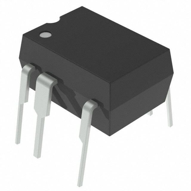
| 描述 | IC OFFLINE SWIT OTP OCP HV 8DIP交流/直流转换器 6 W (85-265 VAC) 9 W (230 VAC) |
| 产品分类 | |
| 品牌 | Power Integrations |
| 产品手册 | |
| 产品图片 |
|
| rohs | 符合RoHS无铅 / 符合限制有害物质指令(RoHS)规范要求 |
| 产品系列 | 电源管理 IC,交流/直流转换器,Power Integrations TNY264PGTinySwitch®-II |
| 数据手册 | |
| 产品型号 | TNY264PG |
| 产品目录页面 | |
| 产品种类 | 交流/直流转换器 |
| 供应商器件封装 | DIP-8B |
| 其它名称 | 596-1255-5 |
| 功率(W) | 9W |
| 包装 | 管件 |
| 商标 | Power Integrations |
| 封装 | Tube |
| 封装/外壳 | 8-DIP(0.300",7.62mm),7 引线 |
| 工作温度 | -40°C ~ 150°C |
| 工厂包装数量 | 50 |
| 标准包装 | 50 |
| 电压-击穿 | 700V |
| 电压-输入 | - |
| 电压-输出 | - |
| 输出隔离 | 隔离 |
| 频率范围 | 124kHz ~ 140kHz |


- 商务部:美国ITC正式对集成电路等产品启动337调查
- 曝三星4nm工艺存在良率问题 高通将骁龙8 Gen1或转产台积电
- 太阳诱电将投资9.5亿元在常州建新厂生产MLCC 预计2023年完工
- 英特尔发布欧洲新工厂建设计划 深化IDM 2.0 战略
- 台积电先进制程称霸业界 有大客户加持明年业绩稳了
- 达到5530亿美元!SIA预计今年全球半导体销售额将创下新高
- 英特尔拟将自动驾驶子公司Mobileye上市 估值或超500亿美元
- 三星加码芯片和SET,合并消费电子和移动部门,撤换高东真等 CEO
- 三星电子宣布重大人事变动 还合并消费电子和移动部门
- 海关总署:前11个月进口集成电路产品价值2.52万亿元 增长14.8%


PDF Datasheet 数据手册内容提取
This product is not recommended for new designs. TNY263-268 TinySwitch-II Family Enhanced, Energy Efficient, Low Power Off-line Switcher Product Highlights + + Optional DC TinySwitch-II Features Reduce System Cost UV Resistor Output • Fully integrated auto-restart for short circuit and open loop fault - protection – saves external component costs Wide-Range • Built-in circuitry practically eliminates audible noise with ordinary High-Voltage dip-varnished transformer DC Input D EN/UV • Programmable line undervoltage detect feature prevents power TinySwitch-II BP on/off glitches – saves external components • Frequency jittering dramatically reduces EMI (~10 dB) S – minimizes EMI filter component costs - • 132 kHz operation reduces transformer size – allows use of PI-2684-061815 EF12.6 or EE13 cores for low cost and small size • Very tight tolerances and negligible temperature variation on key Figure 1. Typical Standby Application. parameters eases design and lowers cost • Lowest component count switcher solution • Expanded scalable device family for low system cost Output Power Table Better Cost/Performance over RCC & Linears 230 VAC ± 15% 85-265 VAC • Lower system cost than RCC, discrete PWM and other Product3 Open Open integrated/hybrid solutions Adapter1 Adapter1 Frame2 Frame2 • Cost effective replacement for bulky regulated linears • Simple ON/OFF control – no loop compensation needed TNY263 P/G 5 W 7.5 W 3.7 W 4.7 W • No bias winding – simpler, lower cost transformer TNY264 P/G 5.5 W 9 W 4 W 6 W • Simple design practically eliminates rework in manufacturing TNY265 P/G 8.5 W 11 W 5.5 W 7.5 W TNY266 P/G 10 W 15 W 6 W 9.5 W EcoSmart™– Extremely Energy Efficient • No load consumption <50 mW with bias winding and TNY267 P/G 13 W 19 W 8 W 12 W <250 mW without bias winding at 265 VAC input TNY268 P/G 16 W 23 W 10 W 15 W • Meets California Energy Commission (CEC), Energy Star, and EU requirements Table 1. Output Power Table. • Ideal for cell-phone charger and PC standby applications Notes: 1. Minimum continuous power in a typical non-ventilated enclosed adapter measured at 50 °C ambient. High Performance at Low Cost 2. Minimum practical continuous power in an open frame design with adequate • High voltage powered – ideal for charger applications heat sinking, measured at 50 °C ambient (See Key Applications • High bandwidth provides fast turn on with no overshoot Considerations). • Current limit operation rejects line frequency ripple 3. Packages: P: DIP-8B, G: SMD-8B. Please see Part Ordering Information. • Built-in current limit and thermal protection improves safety Description TinySwitch™-II integrates a 700 V power MOSFET, oscillator, The fully integrated auto-restart circuit safely limits output power high voltage switched current source, current limit and thermal during fault conditions such as output short circuit or open loop, shutdown circuitry onto a monolithic device. The start-up and reducing component count and secondary feedback circuitry operating power are derived directly from the voltage on the cost. An optional line sense resistor externally programs a line DRAIN pin, eliminating the need for a bias winding and associated undervoltage threshold, which eliminates power down glitches circuitry. In addition, the TinySwitch-II devices incorporate caused by the slow discharge of input storage capacitors present auto-restart, line undervoltage sense, and frequency jittering. An in applications such as standby supplies. The operating innovative design minimizes audio frequency components in the frequency of 132 kHz is jittered to significantly reduce both the simple ON/OFF control scheme to practically eliminate audible quasi-peak and average EMI, minimizing filtering cost. noise with standard taped/varnished transformer construction. www.power.com August 2016 This Product is Covered by Patents and/or Pending Patent Applications.
TNY263-268 BYPASS DRAIN (BP) (D) REGULATOR 5.8 V LINE UNDERVOLTAGE 240 µA 50 µA FAULT BYPASS PIN PRESENT + UNDERVOLTAGE AUTO- RESTART - COUNTER CURRENT 5.8 V LIMIT STATE 4.8 V VILIMIT MACHINE 6.3 V RESET CURRENT LIMIT COMPARATOR ENABLE - + JITTER CLOCK 1.0 V + VT DCMAX THERMAL SHUTDOWN OSCILLATOR ENABLE/ UNDER- 1.0 V VOLTAGE S Q (EN/UV) R Q LEADING EDGE BLANKING SOURCE (S) PI-2643-031715 Figure 2. Functional Block Diagram. Pin Functional Description DRAIN (D) Pin: P Package (DIP-8B) Power MOSFET drain connection. Provides internal operating G Package (SMD-8B) current for both start-up and steady-state operation. BYPASS (BP) Pin: BP 1 8 S (HV RTN) Connection point for a 0.1 µF external bypass capacitor for the internally generated 5.8 V supply. S 2 7 S (HV RTN) ENABLE/UNDERVOLTAGE (EN/UV) Pin: S 3 This pin has dual functions: enable input and line undervoltage EN/UV 4 5 D sense. During normal operation, switching of the power MOSFET is controlled by this pin. MOSFET switching is terminated when a current greater than 240 µA is drawn from this pin. This pin also senses line undervoltage conditions PI-2685-031715 through an external resistor connected to the DC line voltage. If there is no external resistor connected to this pin, Figure 3. Pin Configuration. TinySwitch-II detects its absence and disables the line undervoltage function. SOURCE (HV RTN) Pin: Output MOSFET source connection for high voltage return. SOURCE (S) Pin: Control circuit common, internally connected to output MOSFET source. 2 Rev. J 08/16 www.power.com
TNY263-268 TinySwitch-II Functional Description MOSFET remains off (disabled). Since the sampling is done only at the beginning of each cycle, subsequent changes in TinySwitch-II combines a high voltage power MOSFET switch the EN/UV pin voltage or current during the remainder of the with a power supply controller in one device. Unlike conventional cycle are ignored. PWM (pulse width modulator) controllers, TinySwitch-II uses a simple ON/OFF control to regulate the output voltage. The current limit state machine reduces the current limit by discrete amounts at light loads when TinySwitch-II is likely to The TinySwitch-II controller consists of an oscillator, enable switch in the audible frequency range. The lower current limit circuit (sense and logic), current limit state machine, raises the effective switching frequency above the audio range 5.8 V regulator, BYPASS pin undervoltage circuit, over- and reduces the transformer flux density, including the temperature protection, current limit circuit, leading edge associated audible noise. The state machine monitors the blanking and a 700 V power MOSFET. TinySwitch-II sequence of EN/UV pin voltage levels to determine the load incorporates additional circuitry for line undervoltage sense, condition and adjusts the current limit level accordingly in auto-restart and frequency jitter. Figure 2 shows the functional discrete amounts. block diagram with the most important features. Under most operating conditions (except when close to no- Oscillator load), the low impedance of the source follower keeps the The typical oscillator frequency is internally set to an average voltage on the EN/UV pin from going much below 1.0 V in the of 132 kHz. Two signals are generated from the oscillator: the disabled state. This improves the response time of the maximum duty cycle signal (DC ) and the clock signal that optocoupler that is usually connected to this pin. MAX indicates the beginning of each cycle. 5.8 V Regulator and 6.3 V Shunt Voltage Clamp The TinySwitch-II oscillator incorporates circuitry that The 5.8 V regulator charges the bypass capacitor connected introduces a small amount of frequency jitter, typically 8 kHz to the BYPASS pin to 5.8 V by drawing a current from the peak-to-peak, to minimize EMI emission. The modulation rate voltage on the DRAIN pin whenever the MOSFET is off. The of the frequency jitter is set to 1 kHz to optimize EMI reduction BYPASS pin is the internal supply voltage node for the for both average and quasi-peak emissions. The frequency TinySwitch-II. When the MOSFET is on, the TinySwitch-II jitter should be measured with the oscilloscope triggered at operates from the energy stored in the bypass capacitor. the falling edge of the DRAIN waveform. The waveform in Extremely low power consumption of the internal circuitry Figure 4 illustrates the frequency jitter of the TinySwitch-II. allows TinySwitch-II to operate continuously from current it takes from the DRAIN pin. A bypass capacitor value of 0.1 µF Enable Input and Current Limit State Machine is sufficient for both high frequency decoupling and energy The enable input circuit at the EN/UV pin consists of a low storage. impedance source follower output set at 1.0 V. The current through the source follower is limited to 240 µA. When the In addition, there is a 6.3 V shunt regulator clamping the current out of this pin exceeds 240 µA, a low logic level BYPASS pin at 6.3 V when current is provided to the BYPASS (disable) is generated at the output of the enable circuit. This pin through an external resistor. This facilitates powering of enable circuit output is sampled at the beginning of each cycle TinySwitch-II externally through a bias winding to decrease the on the rising edge of the clock signal. If high, the power no-load consumption to about 50 mW. MOSFET is turned on for that cycle (enabled). If low, the power BYPASS Pin Undervoltage 600 1 The BYPASS pin undervoltage circuitry disables the power 0 19 MOSFET when the BYPASS pin voltage drops below 4.8 V. 4 500 1-0 Once the BYPASS pin voltage drops below 4.8 V, it must rise 4 400 VDRAIN PI-27 back to 5.8 V to enable (turn-on) the power MOSFET. Over Temperature Protection 300 The thermal shutdown circuitry senses the die temperature. The threshold is typically set at 135 °C with 70 °C hysteresis. 200 When the die temperature rises above this threshold the power MOSFET is disabled and remains disabled until the die 100 temperature falls by 70 °C, at which point it is re-enabled. A large hysteresis of 70 °C (typical) is provided to prevent 0 overheating of the PC board due to a continuous fault 136 kHz condition. 128 kHz Current Limit The current limit circuit senses the current in the power 0 5 10 MOSFET. When this current exceeds the internal threshold Time (µs) (I ), the power MOSFET is turned off for the remainder of Figure 4. Frequency Jitter. LIMIT 3 www.power.com Rev. J 08/16
TNY263-268 that cycle. The current limit state machine reduces the current BYPASS pin then rises from 4.8 V to 5.8 V when the line limit threshold by discrete amounts under medium and light undervoltage condition goes away. When the switching of the loads. power MOSFET is disabled in auto-restart mode and a line undervoltage condition exists, the auto-restart counter is The leading edge blanking circuit inhibits the current limit stopped. This stretches the disable time beyond its normal comparator for a short time (t ) after the power MOSFET is 850 ms until the line undervoltage condition ends. LEB turned on. This leading edge blanking time has been set so that current spikes caused by capacitance and secondary- The line undervoltage circuit also detects when there is no side rectifier reverse recovery time will not cause premature external resistor connected to the EN/UV pin (less than termination of the switching pulse. ~2 µA into the pin). In this case the line undervoltage function is disabled. Auto-Restart In the event of a fault condition such as output overload, TinySwitch-II Operation output short circuit, or an open loop condition, TinySwitch-II enters into auto-restart operation. An internal counter clocked TinySwitch-II devices operate in the current limit mode. When by the oscillator gets reset every time the EN/UV pin is pulled enabled, the oscillator turns the power MOSFET on at the low. If the EN/UV pin is not pulled low for 50 ms, the power beginning of each cycle. The MOSFET is turned off when the MOSFET switching is normally disabled for 850 ms (except in current ramps up to the current limit or when the DC limit is MAX the case of line undervoltage condition, in which case it is reached. Since the highest current limit level and frequency of disabled until the condition is removed). The auto-restart a TinySwitch-II design are constant, the power delivered to the alternately enables and disables the switching of the power load is proportional to the primary inductance of the transformer MOSFET until the fault condition is removed. Figure 5 and peak primary current squared. Hence, designing the supply illustrates auto-restart circuit operation in the presence of an involves calculating the primary inductance of the transformer output short circuit. for the maximum output power required. If the TinySwitch-II is appropriately chosen for the power level, the current in the In the event of a line undervoltage condition, the switching of calculated inductance will ramp up to current limit before the the power MOSFET is disabled beyond its normal 850 ms time DC limit is reached. MAX until the line undervoltage condition ends. Enable Function Line Undervoltage Sense Circuit TinySwitch-II senses the EN/UV pin to determine whether or The DC line voltage can be monitored by connecting an not to proceed with the next switching cycle as described external resistor from the DC line to the EN/UV pin. During earlier. The sequence of cycles is used to determine the power-up or when the switching of the power MOSFET is current limit. Once a cycle is started, it always completes the disabled in auto-restart, the current into the EN/UV pin must cycle (even when the EN/UV pin changes state half way exceed 49 µA to initiate switching of the power MOSFET. through the cycle). This operation results in a power supply in During power-up, this is accomplished by holding the BYPASS which the output voltage ripple is determined by the output pin to 4.8 V while the line undervoltage condition exists. The capacitor, amount of energy per switch cycle and the delay of the feedback. 300 VDRAIN PI-2699-030701 Tcvooouhlmtetpa EpugNate rv./i Uon TglVtha tepgh ieeEn Nipsso/ iglUewnsVeas rlp tisishnu a gpsneip gntlnhye aeroa l ruitesetfp dehu rioget nhnv octwhelth aeveg osnelet atcwhgoietenh .pd aoa rwryee fber yrse unpcpel y 200 In a typical implementation, the EN/UV pin is driven by an 100 optocoupler. The collector of the optocoupler transistor is connected to the EN/UV pin and the emitter is connected to 0 the SOURCE pin. The optocoupler LED is connected in series 10 with a Zener diode across the DC output voltage to be V regulated. When the output voltage exceeds the target 5 DC-OUTPUT regulation voltage level (optocoupler LED voltage drop plus Zener voltage), the optocoupler LED will start to conduct, 0 pulling the EN/UV pin low. The Zener diode can be replaced by a TL431 reference circuit for improved accuracy. 0 1000 2000 ON/OFF Operation with Current Limit State Machine Time (ms) The internal clock of the TinySwitch-II runs all the time. At the beginning of each clock cycle, it samples the EN/UV pin to Figure 5. TinySwitch-II Auto-Restart Operation. decide whether or not to implement a switch cycle, and based on the sequence of samples over multiple cycles, it determines 4 Rev. J 08/16 www.power.com
TNY263-268 the appropriate current limit. At high loads, when the EN/UV reduced even further (Figure 9). Only a small percentage of pin is high (less than 240 µA out of the pin), a switching cycle cycles will occur to satisfy the power consumption of the with the full current limit occurs. At lighter loads, when EN/UV power supply. is high, a switching cycle with a reduced current limit occurs. The response time of the TinySwitch-II ON/OFF control At near maximum load, TinySwitch-II will conduct during scheme is very fast compared to normal PWM control. This nearly all of its clock cycles (Figure 6). At slightly lower load, it provides tight regulation and excellent transient response. will “skip” additional cycles in order to maintain voltage regulation at the power supply output (Figure 7). At medium Power Up/Down loads, cycles will be skipped and the current limit will be The TinySwitch-II requires only a 0.1 µF capacitor on the reduced (Figure 8). At very light loads, the current limit will be BYPASS pin. Because of its small size, the time to charge this capacitor is kept to an absolute minimum, typically 0.6 ms. Due to the fast nature of the ON/OFF feedback, there is no overshoot at the power supply output. When an external VEN resistor (2 MΩ) is connected from the positive DC input to the EN/UV pin, the power MOSFET switching will be delayed during power-up until the DC line voltage exceeds the CLOCK threshold (100 V). Figures 10 and 11 show the power-up timing waveform of TinySwitch-II in applications with and without an D external resistor (2 MΩ) connected to the EN/UV pin. MAX During power-down, when an external resistor is used, the power MOSFET will switch for 50 ms after the output loses I regulation. The power MOSFET will then remain off without DRAIN any glitches since the undervoltage function prohibits restart when the line voltage is low. Figure 12 illustrates a typical power-down timing waveform of TinySwitch-II. Figure 13 illustrates a very slow power-down timing waveform of TinySwitch-II as in standby applications. V DRAIN The external resistor (2 MΩ) is connected to the EN/UV pin in this case to prevent unwanted restarts. The TinySwitch-II does not require a bias winding to provide power to the chip, because it draws the power directly from Figure 6. TinySwitch-II Operation at Near Maximum Loading. the DRAIN pin (see Functional Description above). This has V V EN EN CLOCK CLOCK D D MAX MAX I I DRAIN DRAIN V DRAIN V DRAIN Figure 7. TinySwitch-II Operation at Moderately Heavy Loading. Figure 8. TinySwitch-II Operation at Medium Loading. 5 www.power.com Rev. J 08/16
TNY263-268 200 5 1 V 10 EN 100 VDC-INPUT 1-02 8 3 2 CLOCK 0 PI- 10 D MAX V 5 BYPASS 0 I DRAIN 400 200 V DRAIN 0 0 1 2 Time (ms) V DRAIN Figure 11. TinySwitch-II Power-up without Optional External UV Resistor Connected to EN/UV Pin. Figure 9. TinySwitch-II Operation at Very Light Load. 200 PI-2348-021015 100 VDC-INPUT two main benefits. First, for a nominal application, this eliminates the cost of a bias winding and associated 0 components. Secondly, for battery charger applications, the current-voltage characteristic often allows the output voltage 400 to fall close to zero volts while still delivering power. This type of application normally requires a forward-bias winding which 300 has many more associated components. With TinySwitch-II, neither are necessary. For applications that require a very low 200 VDRAIN no-load power consumption (50 mW), a resistor from a bias 100 winding to the BYPASS pin can provide the power to the chip. The minimum recommended current supplied is 750 µA. The 0 BYPASS pin in this case will be clamped at 6.3 V. This method 0 .5 1 will eliminate the power draw from the DRAIN pin, thereby Time (s) Figure 12. Normal Power-down Timing (without UV). 120000 VDC-INPUT 383-021015 200 395-101014 2 2 0 PI- 100 V PI- DC-INPUT 10 0 V 5 BYPASS 400 0 300 400 200 VDRAIN 200 V 100 DRAIN 0 0 0 1 2 0 2.5 5 Time (ms) Time (s) Figure 10. TinySwitch-II Power-up with Optional External UV Figure 13. Slow Power-down Timing with Optional External Resistor (2 MΩ) Connected to EN/UV Pin. (2 MΩ) UV Resistor Connected to EN/UV Pin. 6 Rev. J 08/16 www.power.com
TNY263-268 C8 680 pF Y1 Safety Shield T1 R2 D5 L2 + 5 V 200 kΩ 1 8 1N5819 3.3 µH 500 mA C3 C5 C6 2.2 nF 330 µF 100 µF 16 V 35 V RTN D1 D2 4 5 1N4005 1N4005 R8 D6 270 Ω 1N4937 85-265 3.C3 1µF 3.C3 2µF LTUV8217 10R07 Ω VAC 400 V 400 V RF1 D EN/UV 8.2 Ω TinySwitch-II R9 Fusible TNUY1264 S BP 2NQ3910447 Ω 2R2 3Ω R19B3V99 V R1 C3 VX73. D3 D4 1.2 kΩ 0.1 µF BZ 1N4005 1N4005 C7 10 µF 10 V L1 R4 R6 2.2 mH 1.2 Ω 1 Ω 1/2 W 1/2 W PI-2706-061815 Figure 14. 2.5 W Constant Voltage, Constant Current Battery Charger with Universal Input (85-265 VAC). reducing the no-load power consumption and improving full- also saves the cost of adding a fuse or increasing the power load efficiency. rating of the current sense resistors to survive reverse battery conditions. For applications requiring undervoltage lock out Current Limit Operation (UVLO), such as PC standby, the TinySwitch-II eliminates Each switching cycle is terminated when the DRAIN current several components and saves cost. TinySwitch-II is well reaches the current limit of the TinySwitch-II. Current limit suited for applications that require constant voltage and operation provides good line ripple rejection and relatively constant current output. As TinySwitch-II is always powered constant power delivery independent of input voltage. from the input high voltage, it therefore does not rely on bias winding voltage. Consequently this greatly simplifies designing BYPASS Pin Capacitor chargers that must work down to zero volts on the output. The BYPASS pin uses a small 0.1 µF ceramic capacitor for decoupling the internal power supply of the TinySwitch-II. 2.5 W CV/CC Cell-Phone Charger As an example, Figure 14 shows a TNY264 based 5 V, Application Examples 0.5 A, cellular phone charger operating over a universal input range (85 VAC to 265 VAC). The inductor (L1) forms a π-filter The TinySwitch-II is ideal for low cost, high efficiency power in conjunction with C1 and C2. The resistor R1 damps supplies in a wide range of applications such as cellular phone resonances in the inductor L1. Frequency jittering operation of chargers, PC standby, TV standby, AC adapters, motor TinySwitch-II allows the use of a simple π-filter described control, appliance control and ISDN or a DSL network above in combination with a single low value Y1-capacitor (C8) termination. The 132 kHz operation allows the use of a low to meet worldwide conducted EMI standards. The addition of cost EE13 or EF12.6 core transformer while still providing good a shield winding in the transformer allows conducted EMI to be efficiency. The frequency jitter in TinySwitch-II makes it met even with the output capacitively earthed (which is the possible to use a single inductor (or two small resistors for worst case condition for EMI). The diode D6, capacitor C3 under 3 W applications if lower efficiency is acceptable) in and resistor R2 comprise the clamp circuit, limiting the leakage conjunction with two input capacitors for input EMI filtering. inductance turn-off voltage spike on the TinySwitch-II DRAIN The auto-restart function removes the need to oversize the pin to a safe value. The output voltage is determined by the output diode for short circuit conditions allowing the design to sum of the optocoupler U2 LED forward drop (~1 V), and Zener be optimized for low cost and maximum efficiency. In charger diode VR1 voltage. Resistor R8 maintains a bias current applications, it eliminates the need for a second optocoupler through the Zener diode to ensure it is operated close to the and Zener diode for open loop fault protection. Auto-restart Zener test current. 7 www.power.com Rev. J 08/16
TNY263-268 A simple constant current circuit is implemented using the V up undervoltage threshold is set at 200 VDC, slightly below the BE of transistor Q1 to sense the voltage across the current sense lowest required operating DC input voltage, for start-up at 170 resistor R4. When the drop across R4 exceeds the V of VAC, with doubler. This feature saves several components BE transistor Q1, it turns on and takes over control of the loop by needed to implement the glitch-free turn-off compared with driving the optocoupler LED. Resistor R6 assures sufficient discrete or TinySwitch-II based designs. During turn-on the voltage to keep the control loop in operation down to zero volts rectified DC input voltage needs to exceed 200 V undervoltage at the output. With the output shorted, the drop across R4 and threshold for the power supply to start operation. But, once the R6 (~1.2 V) is sufficient to keep the Q1 and LED circuit active. power supply is on it will continue to operate down to Resistors R7 and R9 limit the forward current that could be 140 V rectified DC input voltage to provide the required hold up drawn through VR1 by Q1 under output short circuit conditions, time for the standby output. due to the voltage drop across R4 and R6. The auxiliary primary side winding is rectified and filtered by D2 10 and 15 W Standby Circuits and C2 to create a 12 V primary bias output voltage for the Figures 15 and 16 show examples of circuits for standby main power supply primary controller. In addition, this voltage is applications. They both provide two outputs: an isolated 5 V used to power the TinySwitch-II via R4. Although not necessary and a 12 V primary referenced output. The first, using TNY266P, for operation, supplying the TinySwitch-II externally reduces the provides 10 W, and the second, using TNY267P, device quiescent dissipation by disabling the internal drain 15 W of output power. Both operate from an input range of 140 derived current source normally used to keep the BYPASS pin VDC to 375 VDC, corresponding to a 230 VAC or 100/115 VAC capacitor (C3) charged. An R4 value of 10 kΩ provides 600 µA with doubler input. The designs take advantage of the line into the BYPASS pin, which is slightly in excess of the current undervoltage detect, auto-restart and higher switching consumption of TinySwitch-II. The excess current is safely frequency of TinySwitch-II. Operation at 132 kHz allows the use clamped by an on-chip active Zener diode to 6.3 V. of a smaller and lower cost transformer core, EE16 for 10 W and EE22 for 15 W. The removal of pin 6 from the 8 pin The secondary winding is rectified and filtered by D3 and C6. DIP TinySwitch-II packages provides a large creepage distance For a 15 W design an additional output capacitor, C7, is which improves reliability in high pollution environments such as required due to the larger secondary ripple currents compared fan cooled power supplies. to the 10 W standby design. The auto-restart function limits output current during short circuit conditions, removing the Capacitor C1 provides high frequency decoupling of the high need to over rate D3. Switching noise filtering is provided by L1 voltage DC supply, only necessary if there is a long trace length and C8. The 5 V output is sensed by U2 and VR1. R5 is used to from the DC bulk capacitors of the main supply. The line sense ensure that the Zener diode is biased at its test current and R6 resistors R2 and R3 sense the DC input voltage for line centers the output voltage at 5 V. undervoltage. When the AC is turned off, the undervoltage detect feature of the TinySwitch-II prevents auto-restart glitches In many cases the Zener regulation method provides sufficient at the output caused by the slow discharge of large storage accuracy (typically ± 6% over a 0 °C to 50 °C temperature capacitance in the main converter. This is achieved by range). This is possible because TinySwitch-II limits the dynamic preventing the TinySwitch-II from switching when the input range of the optocoupler LED current, allowing the Zener diode voltage goes below a level needed to maintain output to operate at near constant bias current. However, if higher regulation, and keeping it off until the input voltage goes above accuracy is required, a TL431 precision reference IC may be the undervoltage threshold, when the AC is turned on again. used to replace VR1. With R2 and R3, giving a combined value of 2 MΩ, the power 8 Rev. J 08/16 www.power.com
TNY263-268 PERFORMANCE SUMMARY Continuous Output Power: 10.24 W C4 Efficiency: ≥ 75% 1 nF Y1 C5 L1 140 - 375 R1 2.2 nF D3 10 µH VDC INPUT 200 kΩ 1 kV 1N5822 2 A +5 V, 2 A 1 10 C6 C8 1000 µF 470 µF 10 V 10 V RTN 2 8 C1 0.01 µF D1 1 kV 1N4005GP 4 VR1 TinySwitch-II BZX79B3V9 U1 R2 TNY266P D2 1 MΩ 5 1N4148 T1 R6 +12 VDC, 20 mA 59 Ω R3 1% 1 MΩ R4 D 10 kΩ C2 EN 82 µF 35 V BP U2 S C3 TLP181Y R5 0.1 µF 680 Ω 50 V 0 V PI-2713-061815 Figure 15. 10 W Standby Supply. PERFORMANCE SUMMARY Continuous Output Power: 15.24 W Efficiency: ≥ 78% C4 1 nF Y1 C5 L1 V1D4C0 -IN 3P7U5 T 10R0 1kΩ 21.2 k nVF SBD5340 103 µAH +5 V, 3 A 1 10 C6 C7 C8 1000 µF 1000 µF 470 µF 2 8 10 V 10 V 10 V RTN C1 0.01 µF D1 1 kV 1N4005GP 4 VR1 TinySwitch-II BZX79B3V9 U1 R2 TNY267P D2 1 MΩ 5 1N4148 T1 +12 VDC, 20 mA R6 R3 59 Ω 1 MΩ 1% R4 U2 D 10 kΩ TLP181Y C2 EN 82 µF BP 35 V S C3 R5 0.1 µF 680 Ω 50 V 0 V PI-2712-061815 Figure 16. 15 W Standby Supply. 9 www.power.com Rev. J 08/16
TNY263-268 Key Application Considerations 1. The minimum DC input voltage is 90 V or higher for 85 VAC input, or 240 V or higher for 230 VAC input or TinySwitch-II vs. TinySwitch 115 VAC input with a voltage doubler. This corresponds to a filter capacitor of 3 µF/W for universal input and 1 µF/W Table 2 compares the features and performance differences for 230 VAC or 115 VAC with doubler input. between the TNY254 device of the TinySwitch-II family with 2. A secondary output of 5 V with a Schottky rectifier diode. the TinySwitch-II family of devices. Many of the new features 3. Assumed efficiency of 77% (TNY267 & TNY268), 75% eliminate the need for or reduce the cost of circuit components. (TNY265 & TNY266) and 73% (TNY263 & TNY264). Other features simplify the design and enhance performance. 4. The parts are board mounted with SOURCE pins soldered to sufficient area of copper to keep the die temperature at Design or below 100 °C. Output Power In addition to the thermal environment (sealed enclosure, Table 1 (front page) shows the practical continuous output ventilated, open frame, etc.), the maximum power capability of power levels that can be obtained under the following TinySwitch-II in a given application depends on transformer conditions: TinySwitch-II vs. TinySwitch TinySwitch TinySwitch-II TinySwitch-II Function TNY254 TNY263-268 Advantages Switching Frequency and 44 kHz ±10% (at 25 °C) 132 kHz ±6% (at 25 °C) • Smaller transformer for low cost Tolerance • Ease of design Temperature Variation +8% +2% • Manufacturability (0-100 °C)** • Optimum design for lower cost Active Frequency Jitter N/A* ±4 kHz • Lower EMI minimizing filter component costs Transformer Audible Noise N/A* Yes–built into controller • Practically eliminates audible noise with ordinary dip Reduction varnished transformer – no special construction or gluing required Line UV Detect N/A* Single resistor • Prevents power on/off glitches programmable Current Limit Tolerance ±11% (at 25 °C) ±7% (at 25 °C) • Increases power capability and Temperature Variation -8% 0% simplifies design for high volume (0-100 °C)** manufacturing Auto-Restart N/A* 6% effective on-time • Limits output short-circuit current to less than full load current • No output diode size penalty • Protects load in open loop fault conditions • No additional components required BYPASS Pin Zener Clamp N/A* Internally clamped to 6.3 V • Allows TinySwitch-II to be powered from a low voltage bias winding to improve efficiency and to reduce on-chip power dissipation DRAIN Creepage at Package 0.037 in. / 0.94 mm 0.137 in. / 3.48 mm • Greater immunity to arcing as a result of dust, debris or other contaminants build-up *Not available. ** See typical performance curves. Table 2. Comparison Between TinySwitch and TinySwitch-II. 10 Rev. J 08/16 www.power.com
TNY263-268 core size and design (continuous or discontinuous), efficiency, The voltage rating of a resistor should be considered for the minimum specified input voltage, input storage capacitance, undervoltage detect (Figure 15: R2, R3) resistors. For 1/4 W output voltage, output diode forward drop, etc., and can be resistors, the voltage rating is typically 200 V continuous, different from the values shown in Table 1. whereas for 1/2 W resistors the rating is typically 400 V continuous. Audible Noise The TinySwitch-II practically eliminates any transformer audio Y-Capacitor noise using simple ordinary varnished transformer construction. The placement of the Y-capacitor should be directly from the No gluing of the cores is needed. The audio noise reduction is primary bulk capacitor positive rail to the common/return accomplished by the TinySwitch-II controller reducing the terminal on the secondary side. Such placement will maximize current limit in discrete steps as the load is reduced. This the EMI benefit of the Y-capacitor and avoid problems in minimizes the flux density in the transformer when switching at common-mode surge testing. audio frequencies. Optocoupler Worst Case EMI & Efficiency Measurement It is important to maintain the minimum circuit path from the Since identical TinySwitch-II supplies may operate at several optocoupler transistor to the TinySwitch-II EN/UV and different frequencies under the same load and line conditions, SOURCE pins to minimize noise coupling. care must be taken to ensure that measurements are made under worst case conditions. When measuring efficiency or The EN/UV pin connection to the optocoupler should be kept EMI verify that the TinySwitch-II is operating at maximum to an absolute minimum (less than 12.7 mm or 0.5 in.), and frequency and that measurements are made at both low and this connection should be kept away from the DRAIN pin high line input voltages to ensure the worst case result is (minimum of 5.1 mm or 0.2 in.). obtained. Output Diode Layout For best performance, the area of the loop connecting the secondary winding, the output diode and the output filter Single Point Grounding capacitor, should be minimized. See Figure 17 for optimized Use a single point ground connection at the SOURCE pin for layout. In addition, sufficient copper area should be provided the BYPASS pin capacitor and the Input Filter Capacitor at the anode and cathode terminals of the diode for adequate (see Figure 17). heatsinking. Primary Loop Area Input and Output Filter Capacitors The area of the primary loop that connects the input filter There are constrictions in the traces connected to the input capacitor, transformer primary and TinySwitch-II together and output filter capacitors. These constrictions are present should be kept as small as possible. for two reasons. The first is to force all the high frequency currents to flow through the capacitor (if the trace were wide Primary Clamp Circuit then it could flow around the capacitor). Secondly, the A clamp is used to limit peak voltage on the DRAIN pin at turn- Constrictions minimize the heat transferred from the TinySwitch-II off. This can be achieved by using an RCD clamp (as shown to the input filter capacitor and from the secondary diode to in Figure 14). A Zener and diode clamp (200 V) across the the output filter capacitor. The common/return (the negative primary or a single 550 V Zener clamp from DRAIN to output terminal in Figure 17) terminal of the output filter SOURCE can also be used. In all cases care should be taken capacitor should be connected with a short, low impedance to minimize the circuit path from the clamp components to the path to the secondary winding. In addition, the common/ transformer and TinySwitch-II. return output connection should be taken directly from the secondary winding pin and not from the Y-capacitor Thermal Considerations connection point. Copper underneath the TinySwitch-II acts not only as a single point ground, but also as a heatsink. The hatched areas PC Board Cleaning shown in Figure 17 should be maximized for good heat sinking Power Integrations does not recommend the use of “no clean” of TinySwitch-II and the same applies to the output diode. flux. EN/UV pin For the most up-to-date information visit the PI website If a line undervoltage detect resistor is used then the resistor at: www.power.com. should be mounted as close as possible to the EN/UV pin to minimize noise pick up. 11 www.power.com Rev. J 08/16
TNY263-268 Safety Spacing Input Filter Capacitor Y1- Capacitor + Output Filter Capacitor T HV r a – PRI n s f o SEC S D r m e TOP VIEW r TinySwitch-II Opto- – DC + coupler OUT C BP BP S EN/UV Maximize hatched copper areas ( ) for optimum heat sinking PI-2707-061815 Figure 17. Recommended Circuit Board Layout for TinySwitch-II with Undervoltage Lock Out Resistor. 12 Rev. J 08/16 www.power.com
TNY263-268 Absolute Maximum Ratings(1,4) DRAIN Voltage .................................. ................ -0.3 V to 700 V Operating Junction Temperature(2) ....................-40 °C to 150 °C DRAIN Peak Current: TNY263......................................400 mA Lead Temperature(3) ....................................................... ..260 °C TNY264.....................................400 mA ....................................TNY265......................................440 mA Notes: TNY266.....................................560 mA 1. All voltages referenced to SOURCE, T = 25 °C. A ....................................TNY267.....................................720 mA 2. Normally limited by internal circuitry. TNY268.....................................880 mA 3. 1/16 in. from case for 5 seconds. EN/UV Voltage .......................................................-0.3 V to 9 V 4. Maximum ratings specified may be applied one at a time, EN/UV Current ...............................................................100 mA without causing permanent damage to the product. BYPASS Voltage .................................................. ..-0.3 V to 9 V Exposure to Absolute Maximum Rating conditions for Storage Temperature .......................................-65 °C to 150 °C extended periods of time may affect product reliability. Thermal Resistance Thermal Resistance: P or G Package: Notes: (q ) ........................... 70 °C/W(2); 60 °C/W(3) 1. Measured on the SOURCE pin close to plastic interface. JA (q )(1) ............................................... 11 °C/W 2. Soldered to 0.36 sq. in. (232 mm2), 2 oz. (610 g/m2) copper clad. JC 3. Soldered to 1 sq. in. (645 mm2), 2 oz. (610 g/m2) copper clad. Conditions SOURCE = 0 V; T = -40 to 125 °C Parameter Symbol J Min Typ Max Units See Figure 18 (Unless Otherwise Specified) Control Functions Average 124 132 140 T = 25 °C Output Frequency f J kHz OSC See Figure 4 Peak-Peak Jitter 8 Maximum Duty Cycle DC S1 Open 62 65 68 % MAX EN/UV Pin Turnoff I T = -40 °C to 125 °C -300 -240 -170 µA Threshold Current DIS J I = -125 µA 0.4 1.0 1.5 EN/UV EN/UV Pin Voltage V V EN I = 25 µA 1.3 2.3 2.7 EN/UV I V = 0 V 430 500 µA S1 EN/UV TNY263 200 250 TNY264 225 270 EN/UV Open DRAIN Supply Current (MOSFET TNY265 245 295 I µA S2 Switching) TNY266 265 320 See Note A, B TNY267 315 380 TNY268 380 460 V = 0 V, TNY263-264 -5.5 -3.3 -1.8 BP I T = 25 °C CH1 J BYPASS Pin Charge See Note C, D TNY265-268 -7.5 -4.6 -2.5 mA Current V = 4 V, TNY263-264 -3.8 -2.0 -1.0 BP I T = 25 °C CH2 J See Note C, D TNY265-268 -4.5 -3.0 -1.5 13 www.power.com Rev. J 08/16
TNY263-268 Conditions SOURCE = 0 V; T = -40 to 125 °C Parameter Symbol J Min Typ Max Units See Figure 18 (Unless Otherwise Specified) Control Functions (cont.) BYPASS Pin V See Note C 5.6 5.85 6.15 V Voltage BP BYPASS Pin V 0.80 0.95 1.20 V Voltage Hysteresis BPH EN/UV Pin Line Under- I T = 25 °C 44 49 54 µA Voltage Threshold LUV J Circuit Protection TNY263 di/dt = 42 mA/µs 195 210 225 T = 25 °C See Note E J TNY264 di/dt = 50 mA/µs 233 250 267 T = 25 °C See Note E J TNY265 di/dt = 55 mA/µs 255 275 295 T = 25 °C See Note E J Current Limit I mA LIMIT TNY266 di/dt = 70 mA/µs 325 350 375 T = 25 °C See Note E J TNY267 di/dt = 90 mA/µs 419 450 481 T = 25 °C See Note E J TNY268 di/dt = 110 mA/µs 512 550 588 T = 25 °C See Note E J See Figure 21 0.65 x Initial Current Limit I mA INIT T = 25 °C I J LIMIT(MIN) Leading Edge T = 25 °C t J 170 215 ns Blanking Time LEB See Note F Current Limit T = 25 °C t J 150 ns Delay ILD See Note F, G Thermal Shutdown 125 135 150 °C Temperature Thermal Shutdown 70 °C Hysteresis Output T = 25 °C 33 38 TNY263 J I = 21 mA D T = 100 °C 50 57 J T = 25 °C 28 32 ON-State TNY264 J R Ω Resistance DS(ON) I = 25 mA D T = 100 °C 42 48 J T = 25 °C 19 22 TNY265 J I = 28 mA D T = 100 °C 29 33 J 14 Rev. J 08/16 www.power.com
TNY263-268 Conditions SOURCE = 0 V; T = -40 to 125 °C Parameter Symbol J Min Typ Max Units See Figure 18 (Unless Otherwise Specified) Output (cont.) T = 25 °C 14 16 TNY266 J I = 35 mA D T = 100 °C 21 24 J T = 25 °C 7.8 9.0 ON-State TNY267 J R Ω Resistance DS(ON) I = 45 mA D T = 100 °C 11.7 13.5 J T = 25 °C 5.2 6.0 TNY268 J I = 55 mA D T = 100 °C 7.8 9.0 J V = 6.2 V, BP TNY263-266 50 OFF-State Drain V = 0 V, I EN/UV µA Leakage Current DSS V = 560 V, TD S= 125 °C TNY267-268 100 J Breakdown V = 6.2 V, V = 0 V, BV BP EN/UV 700 V Voltage DSS See Note H, T = 25 °C J Rise Time t 50 ns R Measured in a Typical Flyback Converter Application Fall Time t 50 ns F Drain Supply 50 V Voltage Output EN/UV Delay t See Figure 20 10 µs EN/UV Output Disable t 0.5 µs Setup Time DST Auto-Restart T = 25 °C t J 50 ms ON-Time AR See Note I Auto-Restart DC 5.6 % Duty Cycle AR NOTES: A. Total current consumption is the sum of I and I when EN/UV pin is shorted to ground (MOSFET not switching) and the sum of S1 DSS I and I when EN/UV pin is open (MOSFET switching). S2 DSS B. Since the output MOSFET is switching, it is difficult to isolate the switching current from the supply current at the DRAIN. An alternative is to measure the BYPASS pin current at 6.1 V. C. BYPASS pin is not intended for sourcing supply current to external circuitry. D. See Typical Performance Characteristics section for BYPASS pin start-up charging waveform. E. For current limit at other di/dt values, refer to Figure 25. F. This parameter is derived from characterization. G. This parameter is derived from the change in current limit measured at 1X and 4X of the di/dt shown in the I specification. LIMIT H. Breakdown voltage may be checked against minimum BV specification by ramping the DRAIN pin voltage up to but not DSS exceeding minimum BV . DSS I. Auto-restart on-time has the same temperature characteristics as the oscillator (inversely proportional to frequency). 15 www.power.com Rev. J 08/16
TNY263-268 470 Ω 5 W S2 470 Ω DEN/UV S1 S 2 MΩ 50 V S S 10 V S BP 150 V 0.1 µF NOTE: This test circuit is not applicable for current limit or output characteristic measurements. PI-2686-031715 Figure 18. TinySwitch-II General Test Circuit. DC MAX (internal signal) tP EN/UV V tEN/UV DRAIN 1 t = P f OSC PI-2364-012699 Figure 19. TinySwitch-II Duty Cycle Measurement. Figure 20. TinySwitch-II Output Enable Timing. 0.8 Figure 21. Current Limit Envelope. 16 Rev. J 08/16 www.power.com
TNY263-268 Typical Performance Characteristics Voltageo 25 C)°1.1 PI-2213-012301 quencyto 25 C)°110...208 PI-2680-012301 akdown malized t1.0 utput Frermalized 00..64 BreNor ONo ( ( 0.2 0.9 0 -50 -25 0 25 50 75 100 125 150 -50 -25 0 25 50 75 100 125 Junction Temperature (°C) Junction Temperature (°C) Figure 22. Breakdown vs. Temperature. Figure 23. Frequency vs. Temperature. ent Limitzed to 25 C)°1001...286 TTTNNNYYY222666347/-226686 PI-2714-031715 d Current Limit 11100.....42086 TNY263 N 4od2ri /mmdtaA =li/z 1esd N Lo2Cirm1um0riatr mel=inz A1ted PI-2697-033104 Currormali0.4 malize 0.4 TTTNNNYYY222666456 557050 mmmAAA/// sss 223575050 mmmAAA N r ( o TNY267 90 mA/ s 450 mA 0.2 N 0.2 TNY268 110 mA/ s 550 mA 0.0 0 -50 0 50 100 150 1 2 3 4 Temperature (°C) Normalized di/dt Figure 24. Current Limit vs. Temperature. Figure 25. Current Limit vs. di/dt. e (V) 765 PI-2240-012301 mA) 320500 STTTTcNNNNaYYYYli2222n6666g3456 F act0112o....r8050s:5 PI-2221-031715 g ( 200 TNY267 3.5 n Volta 43 urrent 150 TNY268 5.5 Pi C SS 2 ain 100 A r P 1 D Y B 50 0 TCASE = 25 °C T = 100 °C CASE 0 0 0.2 0.4 0.6 0.8 1.0 0 2 4 6 8 10 Time (ms) Drain Voltage (V) Figure 26. BYPASS Pin Start-up Waveform. Figure 27. Output Characteristic. 17 www.power.com Rev. J 08/16
TNY263-268 Typical Performance Characteristics (cont.) e (pF) 1100000 PI-2683-033104 323550 STTTTcNNNNaYYYYli2222n6666g3456 F act1112o....r0050s: PI-2225-031715 nc Scaling Factors: W) TNY267 3.5 ta TNY263 1.0 m 20 TNY268 5.5 ci TNY264 1.0 ( Capa TTNNYY226656 12..50 wer 15 n 10 TNY267 3.5 Po ai TNY268 5.5 10 r D 5 1 0 0 100 200 300 400 500 600 0 200 400 600 Drain Voltage (V) Drain Voltage (V) Figure 28. C vs. Drain Voltage. Figure 29. Drain Capacitance Power. OSS holdC) PI-2698-012301 es5 ° r2 Tho e d t ge az oltali Vm er-or dN n( U Junction Temperature (°C) Figure 30. Under-voltage Threshold vs. Temperature. 18 Rev. J 08/16 www.power.com
TNY263-268 PDIP-8B (P Package) ⊕D S .004 (.10) .137 (3.48) Notes: -E- MINIMUM 1. Package dimensions conform to JEDEC specification MS-001-AB (Issue B 7/85) for standard dual-in-line (DIP) package with .300 inch row spacing. 2. Controlling dimensions are inches. Millimeter sizes are shown in parentheses. 3. Dimensions shown do not include mold flash or other .240 (6.10) protrusions. Mold flash or protrusions shall not exceed .260 (6.60) .006 (.15) on any side. 4. Pin locations start with Pin 1, and continue counter-clock- wise to Pin 8 when viewed from the top. The notch and/or dimple are aids in locating Pin 1. Pin 6 is omitted. 5. Minimum metal to metal spacing at the package body for the omitted lead location is .137 inch (3.48 mm). Pin 1 6. Lead width measured at package body. 7. Lead spacing measured with the leads constrained to be .356 (9.05) perpendicular to plane T. -D- .387 (9.83) .057 (1.45) .068 (1.73) (NOTE 6) .125 (3.18) .015 (.38) .145 (3.68) MINIMUM -T- SEATING .008 (.20) PLANE .118 (3.00) .015 (.38) .140 (3.56) .300 (7.62) BSC .100 (2.54) BSC .048 (1.22) (NOTE 7) .053 (1.35) P08B .014 (.36) .300 (7.62) .022 (.56) ⊕T E D S .010 (.25) M .390 (9.91) PI-2551-081716 19 www.power.com Rev. J 08/16
TNY263-268 SMD-8B (G Package) ⊕D S.004 (.10) .137 (3.48) Notes: MINIMUM 1. Controlling dimensions are inches. Millimeter sizes are -E- shown in parentheses. 2. Dimensions shown do not include mold flash or other protrusions. Mold flash or protrusions shall not exceed .420 .006 (.15) on any side. .240 (6.10) .372 (9.45) 3. Pin locations start with Pin 1, .260 (6.60) .388 (9.86) and continue counter-clock- ⊕E S.010 (.25) .046.060 .060.046 wise to Pin 8 when viewed from the top. Pin 6 is omitted. 4. Minimum metal to metal .080 spacing at the package body Pin 1 for the omitted lead location is .137 inch (3.48 mm). Pin 1 .086 5. Lead width measured at .186 package body. .100 (2.54) (BSC) .286 6. D and E are referenced datums on the package body. Solder Pad Dimensions .356 (9.05) -D- .387 (9.83) .057 (1.45) .125 (3.18) .068 (1.73) .145 (3.68) (NOTE 5) .004 (.10) .032 (.81) .048 (1.22) .037 (.94) .053 (1.35) .009 (.23) .004 (.10) .036 (0.91) 0 °-8° .012 (.30) .044 (1.12) G08B PI-2546-081716 Part Ordering Information • TinySwitch Product Family • Series Number • Package Identifier G Plastic Surface Mount SMD-8B P Plastic DIP-8B • Lead Finish Blank Standard (Sn Pb) N Pure Matte Tin (RoHS Compliant) G RoHS Compliant and Halogen Free (P package only) • Tape & Reel and Other Options Blank Standard Configurations TNY 264 G N - TL TL Tape & Reel, 1 k pcs minimum, G Package only. 20 Rev. J 08/16 www.power.com
TNY263-268 Revision Notes Date A – 03/01 Corrected first page spacing and sentence in description describing innovative design. Corrected Frequency Jitter in Figure 4 and Frequency Jitter in Parameter Table. Added last sentence to Over Temperature Protection section. Clarified detecting when there is no external resistor connected to the EN/UV pin. B Corrected Figure 6 and its description in the text. 07/01 Corrected formatting, grammar and style errors in text and figures. Corrected and moved Worst Case EMI & Efficiency Measurement section. Added PC Board Cleaning section. Replaced Figure 21 and SMD-8B Package Drawing. Corrected q for P/G package. JA C Updated Figures 15 and 16 and text description for Zener performance. 04/03 Corrected DIP-8B and SMD-8B Package Drawings. Corrected EN/UV under-voltage threshold in text. D 03/04 Corrected 2 MW connected between positive DC input to EN/UV pin in text and Figures 15 and 16. E Added TNY263 and TNY265. 04/04 F Added lead-free ordering information. 12/04 1) Typographical correction in OFF-STATE Drain Leakage Current parameter condition. G 2) Removed I condition from BV parameter and added new Note H. 04/05 DS DSS 3) Added Note 4 to Absolute Maximum Ratings specifications. H Reformatted document, updated Figures 23 and 24 and Part Ordering Information. 02/09 I Updated with new Brand Style. 06/15 J Updated PDIP-8B (P Package) and SMD-8B (G Package) per PCN-16232. 08/16 21 www.power.com Rev. J 08/16
For the latest updates, visit our website: www.power.com Power Integrations reserves the right to make changes to its products at any time to improve reliability or manufacturability. Power Integrations does not assume any liability arising from the use of any device or circuit described herein. POWER INTEGRATIONS MAKES NO WARRANTY HEREIN AND SPECIFICALLY DISCLAIMS ALL WARRANTIES INCLUDING, WITHOUT LIMITATION, THE IMPLIED WARRANTIES OF MERCHANTABILITY, FITNESS FOR A PARTICULAR PURPOSE, AND NON-INFRINGEMENT OF THIRD PARTY RIGHTS. Patent Information The products and applications illustrated herein (including transformer construction and circuits external to the products) may be covered by one or more U.S. and foreign patents, or potentially by pending U.S. and foreign patent applications assigned to Power Integrations. A complete list of Power Integrations patents may be found at www.power.com. Power Integrations grants its customers a license under certain patent rights as set forth at http://www.power.com/ip.htm. Life Support Policy POWER INTEGRATIONS PRODUCTS ARE NOT AUTHORIZED FOR USE AS CRITICAL COMPONENTS IN LIFE SUPPORT DEVICES OR SYSTEMS WITHOUT THE EXPRESS WRITTEN APPROVAL OF THE PRESIDENT OF POWER INTEGRATIONS. As used herein: 1. A Life support device or system is one which, (i) is intended for surgical implant into the body, or (ii) supports or sustains life, and (iii) whose failure to perform, when properly used in accordance with instructions for use, can be reasonably expected to result in significant injury or death to the user. 2. A critical component is any component of a life support device or system whose failure to perform can be reasonably expected to cause the failure of the life support device or system, or to affect its safety or effectiveness. The PI logo, TOPSwitch, TinySwitch, SENZero, SCALE-iDriver, Qspeed, PeakSwitch, LYTSwitch, LinkZero, LinkSwitch, InnoSwitch, HiperTFS, HiperPFS, HiperLCS, DPA-Switch, CAPZero, Clampless, EcoSmart, E-Shield, Filterfuse, FluxLink, StakFET, PI Expert and PI FACTS are trademarks of Power Integrations, Inc. Other trademarks are property of their respective companies. ©2016, Power Integrations, Inc. Power Integrations Worldwide Sales Support Locations World Headquarters Germany Italy Singapore 5245 Hellyer Avenue Lindwurmstrasse 114 Via Milanese 20, 3rd. Fl. 51 Newton Road San Jose, CA 95138, USA. 80337 Munich 20099 Sesto San Giovanni (MI) #19-01/05 Goldhill Plaza Main: +1-408-414-9200 Germany Italy Singapore, 308900 Customer Service: Phone: +49-895-527-39110 Phone: +39-024-550-8701 Phone: +65-6358-2160 Phone: +1-408-414-9665 Fax: +49-895-527-39200 Fax: +39-028-928-6009 Fax: +65-6358-2015 Fax: +1-408-414-9765 e-mail: eurosales@power.com e-mail: eurosales@power.com e-mail: singaporesales@power.com e-mail: usasales@power.com Germany Japan Taiwan China (Shanghai) HellwegForum 1 Kosei Dai-3 Bldg. 5F, No. 318, Nei Hu Rd., Sec. 1 Rm 2410, Charity Plaza, No. 88 59469 Ense 2-12-11, Shin-Yokohama, Nei Hu Dist. North Caoxi Road Germany Kohoku-ku Taipei 11493, Taiwan R.O.C. Shanghai, PRC 200030 Tel: +49-2938-64-39990 Yokohama-shi, Kanagawa Phone: +886-2-2659-4570 Phone: +86-21-6354-6323 e-mail: igbt-driver.sales@ 222-0033 Japan Fax: +886-2-2659-4550 Fax: +86-21-6354-6325 power.com Phone: +81-45-471-1021 e-mail: taiwansales@power.com e-mail: chinasales@power.com Fax: +81-45-471-3717 India UK e-mail: japansales@power.com China (Shenzhen) #1, 14th Main Road Cambridge Semiconductor, 17/F, Hivac Building, No. 2, Keji Vasanthanagar Korea a Power Integrations company Nan 8th Road, Nanshan District, Bangalore-560052 India RM 602, 6FL Westbrook Centre, Block 5, Shenzhen, China, 518057 Phone: +91-80-4113-8020 Korea City Air Terminal B/D, 159-6 2nd Floor Phone: +86-755-8672-8689 Fax: +91-80-4113-8023 Samsung-Dong, Kangnam-Gu, Milton Road Fax: +86-755-8672-8690 e-mail: indiasales@power.com Seoul, 135-728, Korea Cambridge CB4 1YG e-mail: chinasales@power.com Phone: +82-2-2016-6610 Phone: +44 (0) 1223-446483 Fax: +82-2-2016-6630 e-mail: eurosales@power.com e-mail: koreasales@power.com
Mouser Electronics Authorized Distributor Click to View Pricing, Inventory, Delivery & Lifecycle Information: P ower Integrations: TNY265GN-TL TNY266GN-TL TNY263GN-TL TNY268GN TNY268PN TNY264PN TNY264GN TNY268GN-TL TNY266PN TNY266GN TNY267PN TNY264GN-TL TNY267GN TNY263PN TNY263GN TNY265PN TNY265GN TNY267GN-TL TNY263PG TNY264PG TNY265PG TNY266PG TNY267PG DAK-14A