ICGOO在线商城 > 集成电路(IC) > PMIC - AC-DC 转换器,离线开关 > UCC28610D

 Datasheet下载
- 型号: UCC28610D
- 制造商: Texas Instruments
- 库位|库存: xxxx|xxxx
- 要求:
| 数量阶梯 | 香港交货 | 国内含税 |
| +xxxx | $xxxx | ¥xxxx |
查看当月历史价格
查看今年历史价格
UCC28610D产品简介:
ICGOO电子元器件商城为您提供UCC28610D由Texas Instruments设计生产,在icgoo商城现货销售,并且可以通过原厂、代理商等渠道进行代购。 UCC28610D价格参考¥3.99-¥9.89。Texas InstrumentsUCC28610D封装/规格:PMIC - AC-DC 转换器,离线开关, Converter Offline Flyback Topology 30kHz ~ 133kHz 8-SOIC。您可以下载UCC28610D参考资料、Datasheet数据手册功能说明书,资料中有UCC28610D 详细功能的应用电路图电压和使用方法及教程。
UCC28610D 是德州仪器(Texas Instruments)推出的一款高性能、高集成度的离线式开关电源控制器,主要应用于AC-DC转换器领域。该器件适用于多种应用场景,尤其在需要高效、可靠且紧凑设计的电源系统中表现出色。

 主要应用场景包括:

1. 消费电子设备:
   - UCC28610D 广泛应用于智能手机、平板电脑、笔记本电脑等便携式设备的充电器和适配器中。它能够提供稳定的输出电压和电流,确保设备安全充电。
   - 家用电器如电视、音响系统、智能家居设备等也需要高效的电源管理,UCC28610D 可以满足这些设备对电源稳定性和效率的要求。

2. 工业控制与自动化:
   - 在工业环境中,UCC28610D 可用于各种电源模块,为PLC(可编程逻辑控制器)、传感器、执行器等提供可靠的电源支持。其高效率和低待机功耗特性有助于减少能源浪费,提升系统的整体性能。
   - 工业级电源供应器、不间断电源(UPS)等设备也常常采用该芯片,以确保在复杂工况下的稳定运行。

3. 通信基础设施:
   - 通信基站、路由器、交换机等网络设备需要稳定的电源供应,UCC28610D 可以为这些设备提供高效、可靠的电源解决方案。它具备良好的抗干扰能力和宽输入电压范围,适应不同的电网环境。
   - 数据中心的服务器和存储设备同样依赖于高效的电源管理系统,UCC28610D 的高集成度和灵活性使其成为理想选择。

4. 医疗设备:
   - 医疗仪器如监护仪、超声设备、X光机等对电源的精度和稳定性有严格要求。UCC28610D 能够提供精确的电压调节,并具备过压、过流保护功能,确保医疗设备的安全运行。
   - 便携式医疗设备如血糖仪、血压计等也需要高效的小型化电源方案,UCC28610D 的紧凑设计正好满足这一需求。

总之,UCC28610D 凭借其卓越的性能和广泛的适用性,在众多领域中发挥着重要作用,是现代电源设计的理想选择。
| 参数 | 数值 |
| 产品目录 | 集成电路 (IC)半导体 |
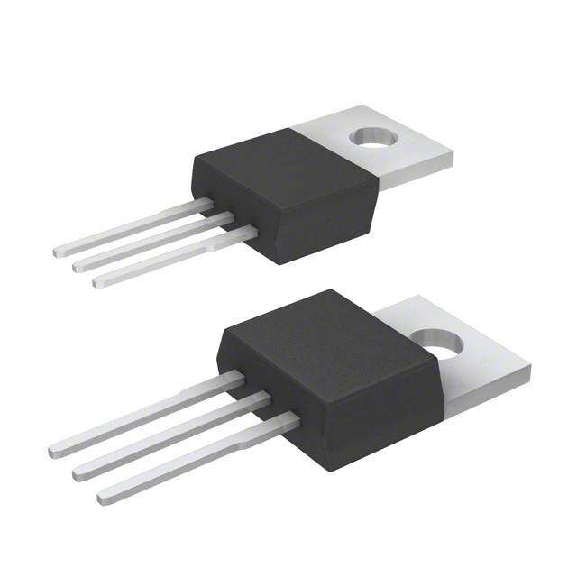
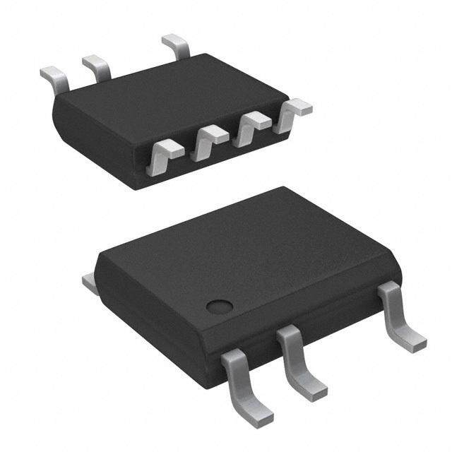
| 描述 | IC CTLR PWM GREEN MODE 8SOIC交流/直流转换器 25-90W Cascoded Fly back Pwr Sply Cntrlr |
| DevelopmentKit | UCC28610EVM-474 |
| 产品分类 | |
| 品牌 | Texas Instruments |
| 产品手册 | http://www.ti.com/litv/slus888f |
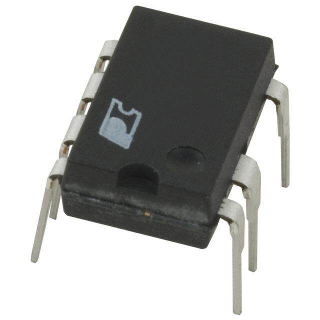
| 产品图片 |
|
| rohs | 符合RoHS无铅 / 符合限制有害物质指令(RoHS)规范要求 |
| 产品系列 | 电源管理 IC,交流/直流转换器,Texas Instruments UCC28610D- |
| 数据手册 | |
| 产品型号 | UCC28610D |
| 产品种类 | 交流/直流转换器 |
| 供应商器件封装 | 8-SOIC |
| 其它名称 | 296-34756-5 |
| 功率(W) | 65W |
| 包装 | 管件 |
| 占空比-最大 | - |
| 商标 | Texas Instruments |
| 安装风格 | SMD/SMT |
| 封装 | Tube |
| 封装/外壳 | 8-SOIC(0.154",3.90mm 宽) |
| 封装/箱体 | SOIC-8 |
| 工作温度 | -40°C ~ 125°C |
| 工作温度范围 | - 40 C to + 125 C |
| 工厂包装数量 | 75 |
| 开关频率 | 30 kHz to 133 kHz |
| 拓扑结构 | Flyback |
| 标准包装 | 75 |
| 电压-击穿 | - |
| 电压-输入 | 9 V ~ 20 V |
| 电压-输出 | - |
| 电源电流 | 3 mA |
| 类型 | Current Mode PWM Controllers |
| 系列 | UCC28610 |
| 绝缘 | Isolated |
| 输入/电源电压—最大值 | 20 V |
| 输入/电源电压—最小值 | 9 V |
| 输出功率 | 65 W |
| 输出电压 | - |
| 输出电流 | 5 A |
| 输出端数量 | 1 Output |
| 输出隔离 | 隔离 |
| 配用 | /product-detail/zh/UCC28610EVM-474/296-31343-ND/2262073 |
| 频率范围 | 30kHz ~ 133kHz |


- 商务部:美国ITC正式对集成电路等产品启动337调查
- 曝三星4nm工艺存在良率问题 高通将骁龙8 Gen1或转产台积电
- 太阳诱电将投资9.5亿元在常州建新厂生产MLCC 预计2023年完工
- 英特尔发布欧洲新工厂建设计划 深化IDM 2.0 战略
- 台积电先进制程称霸业界 有大客户加持明年业绩稳了
- 达到5530亿美元!SIA预计今年全球半导体销售额将创下新高
- 英特尔拟将自动驾驶子公司Mobileye上市 估值或超500亿美元
- 三星加码芯片和SET,合并消费电子和移动部门,撤换高东真等 CEO
- 三星电子宣布重大人事变动 还合并消费电子和移动部门
- 海关总署:前11个月进口集成电路产品价值2.52万亿元 增长14.8%


PDF Datasheet 数据手册内容提取
Product Sample & Technical Tools & Support & Reference Folder Buy Documents Software Community Design UCC28610 SLUS888G–JANUARY2009–REVISEDSEPTEMBER2015 UCC28610 Green-Mode Flyback Controller 1 Features 3 Description • CascodedConfigurationAllowsFullyIntegrated The UCC28610 brings a new level of performance 1 and reliability to the AC and DC consumer power CurrentControlWithoutExternalSenseResistor supplysolution. • FastStartUpWithLowStandbyPowerAchieved byCascodeConfiguration A PWM modulation algorithm varies both the switching frequency and primary current while • FrequencyandPeakCurrentModulationfor maintaining discontinuous or transition mode OptimumEfficiencyOverEntireOperatingRange operation over the entire operating range. Combined • Green-Mode(GM)BurstSwitchingPackets with a cascoded architecture, these innovations result ImproveNo-LoadEfficiency in efficiency, reliability, and system cost • AdvancedOvercurrentProtectionLimitsRMS improvements over a conventional flyback architecture. InputandOutputCurrents • ThermalShutdown The UCC28610 offers a predictable maximum power threshold and a timed response to an overload, • TimedOverloadWithRetryorLatch-Off allowing safe handling of surge power requirements. Response Overload fault response is user-programmed for retry • ProgrammableOpto-LessOutputOvervoltage or latch-off mode. Additional protection features Protection include output overvoltage detection, programmable • FastLatchedFaultRecovery maximumon-time,andthermalshutdown. • 8-PinSOICPackageand8-PinPDIPLead-Free DeviceInformation(1) Packages PARTNUMBER PACKAGE BODYSIZE(NOM) 2 Applications SOIC(8) 4.90mmx3.91mm UCC28610 PDIP(8) 9.81mmx6.35mm • UniversalInputACandDCAdapters,12to65W (1) For all available packages, see the orderable addendum at • HighEfficiencyHousekeepingandAuxillary theendofthedatasheet. PowerSupplies • OfflineBatteryChargers • ConsumerElectronics(DVDPlayers,Set-Top Boxes,DTV,Gaming,Printers) SimplifiedApplicationSchematic + VIN VOUT AC - UCC28610 MOT VGG CL DRV ZCD GND FB VDD 1 An IMPORTANT NOTICE at the end of this data sheet addresses availability, warranty, changes, use in safety-critical applications, intellectualpropertymattersandotherimportantdisclaimers.PRODUCTIONDATA.
UCC28610 SLUS888G–JANUARY2009–REVISEDSEPTEMBER2015 www.ti.com Table of Contents 1 Features.................................................................. 1 7.3 FeatureDescription.................................................13 2 Applications........................................................... 1 7.4 DeviceFunctionalModes........................................18 3 Description............................................................. 1 8 ApplicationandImplementation........................ 19 4 RevisionHistory..................................................... 2 8.1 ApplicationInformation............................................19 8.2 TypicalApplication .................................................31 5 PinConfigurationandFunctions......................... 4 9 PowerSupplyRecommendations...................... 39 6 Specifications......................................................... 5 10 Layout................................................................... 39 6.1 AbsoluteMaximumRatings .....................................5 6.2 ESDRatings..............................................................5 10.1 LayoutGuidelines.................................................39 6.3 RecommendedOperatingConditions.......................5 10.2 LayoutExample....................................................40 6.4 ThermalInformation..................................................6 11 DeviceandDocumentationSupport................. 42 6.5 ElectricalCharacteristics...........................................6 11.1 CommunityResources..........................................42 6.6 TypicalCharacteristics..............................................9 11.2 Trademarks...........................................................42 7 DetailedDescription............................................ 12 11.3 ElectrostaticDischargeCaution............................42 7.1 Overview.................................................................12 11.4 Glossary................................................................42 7.2 FunctionalBlockDiagram.......................................13 12 Mechanical,Packaging,andOrderable Information........................................................... 42 4 Revision History NOTE:Pagenumbersforpreviousrevisionsmaydifferfrompagenumbersinthecurrentversion. ChangesfromRevisionF(November2014)toRevisionG Page • AddedPinConfigurationandFunctionssection,ESDRatingtable,FeatureDescriptionsection,DeviceFunctional Modes,ApplicationandImplementationsection,PowerSupplyRecommendationssection,Layoutsection,Device andDocumentationSupportsection,andMechanical,Packaging,andOrderableInformationsection .............................. 1 ChangesfromRevisionE(September2012)toRevisionF Page • Changedupdatedtypicalapplicationdrawingonfirstpage................................................................................................... 1 • AddedThermalInformationSection....................................................................................................................................... 5 • ChangedESDRating,HumanBodyModelfrom2000Vto1500V...................................................................................... 5 • ChangedElectricalCharacteristicsFB=0VtoIFB=10µA................................................................................................. 6 • ChangedVoltageofCLpinmaxvaluefrom1.05Vto1.10V............................................................................................... 7 • ChangedI rangeforGreenMode(GM)modulationminvaluefrom50µAto45µA......................................................... 7 FB • ChangedZCDlowclampvoltageminvaluefrom-200mVto-220mV................................................................................. 7 • ChangedElectricalCharacteristicsFB=0VtoIFB=10µA................................................................................................. 7 • ChangedElectricalCharacteristicsFB=0VtoIFB=10µA................................................................................................. 8 • ChangedFigure1................................................................................................................................................................... 8 • ChangedSymplifiedBlockDiagram .................................................................................................................................... 11 • ChangedFigure20............................................................................................................................................................... 16 • ChangedHighFrequencyRingingSolutions,(a)ferritechip,(b)CDRVand(c)RG-OFFdrawing.................................... 17 • ChangedBasicFlybackConverterandWaveformsatPeakLoadandMinimumV Voltagedrawing........................... 19 BULK • ChangedStart-UpCurrentsfortheCascodeArchitecturedrawing..................................................................................... 22 • ChangedFeedbackFunctiontext......................................................................................................................................... 23 • ChangedFBDetailsdrawing................................................................................................................................................ 24 • ChangedModulationControlBlocksdrawing....................................................................................................................... 25 • ChangedControlDiagramwithOperatingModesdrawing.................................................................................................. 26 • ChangedRecommendedOperatingConditionsApplicationdrawing.................................................................................. 31 • ChangedBasicFlybackConverterandWaveformsatPeakLoadandMinimumV Voltagedrawing........................... 34 BULK 2 SubmitDocumentationFeedback Copyright©2009–2015,TexasInstrumentsIncorporated ProductFolderLinks:UCC28610
UCC28610 www.ti.com SLUS888G–JANUARY2009–REVISEDSEPTEMBER2015 • ChangedFeedbackFunctiontext......................................................................................................................................... 35 • ChangedFBDetailsdrawing................................................................................................................................................ 36 ChangesfromRevisionD(January2011)toRevisionE Page • ChangedSymplifiedBlockDiagram .................................................................................................................................... 11 ChangesfromRevisionC(January2009)toRevisionD Page • DeletedEquation7 .............................................................................................................................................................. 20 • DeletedEquation7 .............................................................................................................................................................. 34 Copyright©2009–2015,TexasInstrumentsIncorporated SubmitDocumentationFeedback 3 ProductFolderLinks:UCC28610
UCC28610 SLUS888G–JANUARY2009–REVISEDSEPTEMBER2015 www.ti.com 5 Pin Configuration and Functions DPackage PPackage 8-PinSOIC 8-PinPDIP TopView TopView FB 1 8 VDD FB 1 8 VDD ZCD 2 7 GND ZCD 2 7 GND CL 3 6 DRV CL 3 6 DRV MOT 4 5 VGG MOT 4 5 VGG PinFunctions PIN I/O DESCRIPTION NAME NO. (CurrentLimit)Thispinprogramsthepeakprimaryinductorcurrentthatisreachedeachswitchingcycle.Program CL 3 I witharesistorbetweenCLandGND. (DRiVe)ThispindrivesthesourceofanexternalhighvoltagepowerMOSFET.TheDRVpincarriesthefull DRV 6 O primarycurrentoftheconverter.ConnectaSchottkydiodebetweenDRVandVDDtoprovideinitialbiasatstartup. (FeedBack)TheFBcurrent,I ,commandstheoperatingmodeoftheUCC28610.TheFBvoltageisalways0.7V. FB 1 I FB Thispinonlydetectscurrent. (GrouND)ThispinisthecurrentreturnterminalforboththeanalogandpowersignalsintheUCC28610.This GND 7 — terminalcarriesthefullprimarycurrentoftheconverter.Separatethereturnpathofthebulkcapacitorfromthe returnpathofFB,ZCD,MOT,andCL. (MaximumOnTime)Thispinhasthreefunctions: 1. MOTprogramstheallowedmaximumon-time,t ,oftheinternaldriver. MOT 2. MOT programs the converter’s reaction to overload and power input under-voltage conditions with either a MOT 4 I shutdown/retryresponseoralatch-offresponse. 3. MOTcanbeusedtoexternallyshutdownthepowersupplybypullingMOTtoGND.Whenthepinisreleased, theconverterwillstartafterarestartdelay,t . RETRY Functions1and2areprogrammedwitharesistorbetweenMOTandGND. ThisisthebiassupplypinfortheUCC28610.Itcanbederivedfromanexternalsourceoranauxiliarywinding. VDD 8 — Thispinmustbedecoupledwitha0.1-μFceramiccapacitorplacedbetweenVDDandGND,asclosetothedevice aspossible. ThispinprovidesaDCvoltageforthegateoftheexternalhighvoltageMOSFET.Thispinmustbedecoupledwith VGG 5 — a0.1-μFceramiccapacitorplacedbetweenVGGandGND,asclosetothedeviceaspossible.Thispinalso initiatesstart-upbiasthroughalargevalueresistorthatisconnectedtotheinputbulkvoltage. (ZeroCurrentDetection)Thispinhastwofunctions: 1. ZCDsensesthetransformerresetbasedonavalidzerocurrentdetectionsignal. ZCD 2 I 2. ZCDprogramstheoutputOverVoltageProtection(OVP)featureusingaresistivedividerontheprimaryside biaswindingoftheFlybacktransformer. 4 SubmitDocumentationFeedback Copyright©2009–2015,TexasInstrumentsIncorporated ProductFolderLinks:UCC28610
UCC28610 www.ti.com SLUS888G–JANUARY2009–REVISEDSEPTEMBER2015 6 Specifications 6.1 Absolute Maximum Ratings AllvoltagesarewithrespecttoGND,–40°C<T =T <125°C,allcurrentsarepositiveintoandnegativeoutofthespecified J A terminal(unlessotherwisenoted) (1) MIN MAX UNIT VDD –0.5 25 DRV,duringconduction –0.5 2.0 DRV,duringnon-conduction 20 Inputvoltagerange VGG (2) –0.5 16 V ZCD,MOT,CL (3) –0.5 7 FB (3) –0.5 1.0 VDD–VGG –7 10 Continuousinputcurrent I (2) 10 VGG mA Inputcurrentrange I ,I ,I ,I (3) –3 1 ZCD MOT CL FB DRV -5 Peakoutputcurrent A DRV,pulsed200ns,2%dutycycle –5 1.5 T Operatingjunctiontemperature, –40 150 °C J LeadTemperature(soldering,10sec.) 260 °C T Storagetemperaturerange –65 150 °C stg (1) Thesearestressratingsonly.Stressbeyondtheselimitsmaycausepermanentdamagetothedevice.Functionaloperationofthe deviceattheseoranyconditionsbeyondthoseindicatedunderRecommendedOperatingConditionsisnotimplied.Exposureto absolutemaximumratedconditionsforextendedperiodsoftimemayaffectdevicereliability (2) VoltageonVGGisinternallyclamped.Theclamplevelvarieswithoperatingconditions.Innormaluse,VGGiscurrentfedwiththe voltageinternallylimited (3) Innormaluse,MOT,CL,ZCD,andFBareconnectedtoresistorstoGNDandinternallylimitedinvoltageswing 6.2 ESD Ratings VALUE UNIT Humanbodymodel(HBM),perANSI/ESDA/JEDECJS-001,allpins (1) 1500 V(ESD) Electrostaticdischarge Chargeddevicemodel(CDM),perJEDECspecificationJESD22-C101, 500 V allpins (2) (1) JEDECdocumentJEP155statesthat500-VHBMallowssafemanufacturingwithastandardESDcontrolprocess. (2) JEDECdocumentJEP157statesthat250-VCDMallowssafemanufacturingwithastandardESDcontrolprocess. 6.3 Recommended Operating Conditions Unlessotherwisenoted,allvoltagesarewithrespecttoGND,-40°C<T =T <125°C.Componentsreference,Figure34. J A MIN MAX UNIT VDD Inputvoltage 9 20 V VGG Inputvoltagefromlow-impedancesource 9 13 V I Inputcurrentfromahigh-impedancesource 10 2000 μA VGG Shutdown/Retrymode 25 100 kΩ R ResistortoGND MOT Latch-offmode 150 750 kΩ R ResistortoGND 24.3 100 kΩ CL R Resistortoauxiliarywinding 50 200 kΩ ZCD1 C VGGcapacitor 33 200 nF VGG C VDDbypasscapacitor,ceramic 0.1 1 μF BP Copyright©2009–2015,TexasInstrumentsIncorporated SubmitDocumentationFeedback 5 ProductFolderLinks:UCC28610
UCC28610 SLUS888G–JANUARY2009–REVISEDSEPTEMBER2015 www.ti.com 6.4 Thermal Information UCC28610 THERMALMETRIC (1) D(SOIC) P(PDIP) UNIT 8PINS 8PINS R Junction-to-ambientthermalresistance 117.5 56.3 °C/W θJA R Junction-to-case(top)thermalresistance 63.7 45.7 °C/W θJC(top) R Junction-to-boardthermalresistance 57.8 33.5 °C/W θJB ψ Junction-to-topcharacterizationparameter 15.3 22.9 °C/W JT ψ Junction-to-boardcharacterizationparameter 57.3 33.4 °C/W JB (1) Formoreinformationabouttraditionalandnewthermalmetrics,seetheSemiconductorandICPackageThermalMetricsapplication report,SPRA953. 6.5 Electrical Characteristics Unlessotherwisestated:VDD=12V,VGG=12V,ZCD=1V,I =10µA,GND=0V,a0.1-μFcapacitorbetweenVDD FB andGND,a0.1-μFcapacitorbetweenVGGandGND,R =33.2kΩ,R =380kΩ,–40°C<T <+125°C,T =T CL MOT A J A PARAMETER TESTCONDITIONS MIN TYP MAX UNIT VDDandVGGSUPPLY VGG VGGvoltage,operating VDD=14V,I =2.0mA 13 14 15 V (OPERATING) VGG VGG VGGvoltage,PWMdisabled VDD=12V,I =15μA,I =350μA 15 16 17 V (DISABLED) VGG FB RiseinVGGclampingvoltage ΔVGG VGG –VGG 1.75 2.00 2.15 V duringUVLO,GM,orFault (DISABLED) (OPERATING) VGG=VGG -100mV,VDD=12 I VGGshuntregulatorcurrent (DISABLED) 6 10 μA VGG(SREG) V ΔVGG VGGshuntloadregulation 10μA≤I ≤5mA,I =350μA 125 200 mV (SREG) VGG FB VGG VGGLDOregulationvoltage VDD=20V,I =–2mA 13 V (LREG) VGG VGG VGGLDODropoutVoltage VDD–VGG,VDD=11V,I =–2mA 1.5 2 2.5 V (LREG,DO) VGG VDD UVLOturn-onthreshold 9.7 10.2 10.7 V (ON) VDD UVLOturn-offthreshold 7.55 8 8.5 V (OFF) ΔVDD UVLOhysteresis 1.9 2.2 2.5 V (UVLO) I Operatingcurrent VDD=20V 2.5 3 3.7 mA VDD(OPERATING) I Idlecurrentbetweenbursts I =350μA 550 900 μA VDD(GM) FB I CurrentforVDD<UVLO VDD=VDD –100mV,increasing 225 310 μA VDD(UVLO) (ON) VDDSwitchonresistance,DRVto R VGG=12V,VDD=7V,I =50mA 4 10 Ω DS,ON(VDD) VDD DRV VDD VDDforfaultlatchreset 5.6 6 6.4 V (FAULTRESET) MODULATION t (1) Minimumswitchingperiod, I =0μA, (1) 7.125 7.5 7.875 μs S(HF) frequencymodulation(FM)mode FB Maximumswitchingperiod, t (1) reachedatendofFMmodulation I =I –20μA,(1) 31 34 38 μs S(LF) FB FB,CNR3 range Maximumpeakdrivercurrentover IFB=0μA,RCL=33.2kΩ 2.85 3 3.15 I A DRVpk(max) amplitudemodulation(AM)range I =0μA,R =100kΩ 0.80 0.90 1.0 FB CL Minimumpeakdrivercurrent I +10μA,R =33.2kΩ 0.7 0.85 1.1 FB,CNR2 CL I reachedatendofAMmodulation A DRVpk(min) range IFB,CNR2+10μA,RCL=100kΩ 0.2 0.33 0.5 K Maximumpowerconstant I =3A 0.54 0.60 0.66 W/μH P DRVpk(max) Minimumpeakdriverindependent I R =OPEN 0.3 0.45 0.6 A DRVpk(absmin) ofR orAMcontrol CL CL (1) t setsaminimumswitchingperiod.FollowingthestartingedgeofaPWMontime,undernormalconditions,thenextontimeisinitiated S followingthefirstzerocrossingatZCDaftert .Thevalueoft ismodulatedbyI betweenaminimumoft andamaximumof S S FB S(HF) t Innormaloperation,t setsthemaximumoperatingfrequencyofthepowersupplyandt setstheminimumoperating S(LF) S(HF) S(LF) frequencyofthepowersupply. 6 SubmitDocumentationFeedback Copyright©2009–2015,TexasInstrumentsIncorporated ProductFolderLinks:UCC28610
UCC28610 www.ti.com SLUS888G–JANUARY2009–REVISEDSEPTEMBER2015 Electrical Characteristics (continued) Unlessotherwisestated:VDD=12V,VGG=12V,ZCD=1V,I =10µA,GND=0V,a0.1-μFcapacitorbetweenVDD FB andGND,a0.1-μFcapacitorbetweenVGGandGND,R =33.2kΩ,R =380kΩ,–40°C<T <+125°C,T =T CL MOT A J A PARAMETER TESTCONDITIONS MIN TYP MAX UNIT Leadingedgecurrentlimitblanking I =0μA,R =100kΩ,1.2-Apull-upon t FB CL 120 220 450 ns BLANK(Ilim) time DRV I =0μA 2.94 3 3.06 FB V VoltageofCLpin V CL I =(I –20μA) (1) 0.95 1.00 1.10 FB FB,CNR3 I (2) I rangeforFMmodulation IFBincreasing,tS=tS(LF), 145 165 195 μA FB,CNR1 FB I =I DRVpk DRVpk(max) I –I t =t ,I rangesfrom (F2B),CNR2 FB,CNR1 IFBrangeforAMmodulation IS S(LF) tDoRIVpk 35 45 65 μA DRVpk(max) DRVpk(min) I –I I rangeforGreenMode(GM) I increasinguntilPWMactionisdisabled (F2B),CNR3 FB,CNR2 mFBodulation eFnBteringaburst-offstate 45 70 90 μA I hysteresisduringGM FB I (2) modulationtoenterburstonand I decreasingfromaboveI 10 25 40 μA FB,GM-HYST FB FB,CNR3 offstates V VoltageofFBpin I =10μA 0.34 0.7 0.84 V FB FB ZEROCROSSINGDETECTION ZCDhightolowgeneratesswitchingperiod ZCD ZCDzerocrossingthreshold 5 20 50 mV (TH) (t hasexpired) S ZCD ZCDlowclampvoltage I =–10μA -220 -160 -100 mV (CLAMP) ZCD ZCDvoltagethresholdtoenable Driverswitchingperiodsgeneratedatstart ZCD 0.1 0.15 0.2 V (START) theinternalstarttimer timerrate DelayfromzerocrossingtoDriver t 150-Ωpull-upto12-VonDRV 150 ns DLY(ZCD) turn-on Waittimeforzerocrossing Driverturn-onedgegeneratedfollowingt t S 2 2.4 2.8 WAIT(ZCD) detection withpreviouszerocrossingdetected μs t Startertime-outperiod ZCD=0V 150 240 300 ST DRIVER R Driveron-resistance I =4.0A 90 190 mΩ DS(on)(DRV) DRV I Driveroff-leakagecurrent DRV=12V 1.5 20 μA DRV(OFF) R High-sidedriveron-resistance I =–50mA 6 11 Ω DS(on)(HSDRV) DRV I DRVbulkdischargecurrent VDDopen,DRV=12V,Faultlatchset 2 2.8 3.6 mA DRV(DSCH) OVERVOLTAGEFAULT ZCD OvervoltagefaultthresholdatZCD Faultlatchset 4.85 5 5.15 V (OVP) ZCDblankingandOVPsample t 0.6 1 1.7 μs BLANK(OVP) timefromtheturn-offedgeofDRV I ZCDInputbiascurrent ZCD=5V -0.1 -0.05 0.1 μA ZCD(bias) OVERLOADFAULT Currenttotriggeroverloaddelay I 0 1.5 3 μA FB(OL) timer t Delaytooverloadfault I =0Acontinuously 200 250 325 ms OL FB Retrydelayinretrymodeorafter t R =76kΩ 750 ms RETRY shutdowncommand MOT R BoundaryRMOTbetweenlatch-off See (3) 100 120 150 kΩ MOT(TH) andretrymodes SHUTDOWNTHRESHOLD MOT Shutdown-Retrythreshold MOThightolow 0.7 1 1.3 V (SR) MOTcurrentwhenMOTispulled I MOT=1V –600 –450 –300 μA MOT low (2) RefertoFigure1. (3) Alatch-offorashutdownandretryfaultresponsetoasustainedoverloadisselectedbytherangeofR . MOT Toselectthelatch-offmode,R shouldbegreaterthan150kΩandt isgivenbyR ×(1.0×10⁻¹¹). MOT MOT MOT Toselecttheshutdown-retrymode,R shouldbelessthan100kΩandt isgivenbyR ×(5.0×10⁻¹¹). MOT MOT MOT Copyright©2009–2015,TexasInstrumentsIncorporated SubmitDocumentationFeedback 7 ProductFolderLinks:UCC28610
UCC28610 SLUS888G–JANUARY2009–REVISEDSEPTEMBER2015 www.ti.com Electrical Characteristics (continued) Unlessotherwisestated:VDD=12V,VGG=12V,ZCD=1V,I =10µA,GND=0V,a0.1-μFcapacitorbetweenVDD FB andGND,a0.1-μFcapacitorbetweenVGGandGND,R =33.2kΩ,R =380kΩ,–40°C<T <+125°C,T =T CL MOT A J A PARAMETER TESTCONDITIONS MIN TYP MAX UNIT MAXIMUMONTIME Latch-OFF R =383kΩ 3.43 3.83 4.23 MOT t μs MOT Shutdown-retry R =76kΩ 3.4 3.8 4.2 MOT MOT MOTvoltage 2.7 3 3.3 V THERMALSHUTDOWN T (4) Shutdowntemperature T,temperaturerising (4) 165 °C SD J TSD_HYS (4) Hysteresis T(4J),temperaturefalling,degreesbelowTSD 15 °C (4) Thermalshutdownoccursattemperatureshigherthanthenormaloperatingrange.Deviceperformanceatornearthermalshutdown temperatureisnotspecifiedorassured. % - nt Curre FM I AMI GM I FB,CNR1 FB,CNR2 FB,CNR3 V R (165mA) (210mA) (280mA) D 100 k a Pe I -I m FB,CNR3 FB,CNR2 u (70mA) m xi a M of nt e erc 33 P - RV,PK ID 133 I -I FB,CNR2 FB,CNR1 (45mA) - y c n e u q e ngFrkHz IGM,HYST hi (25mA) c wit S - fS 30 0 50 100 150 200 250 300 I -Feedback Current-μA FB Figure1. FBElectricalConditionDetail 8 SubmitDocumentationFeedback Copyright©2009–2015,TexasInstrumentsIncorporated ProductFolderLinks:UCC28610
UCC28610 www.ti.com SLUS888G–JANUARY2009–REVISEDSEPTEMBER2015 6.6 Typical Characteristics Unlessotherwisestated:VDD=12V,VGG=12V,ZCD=1V,I =10µA,GND=0V,a0.1-μFcapacitorbetweenVDD FB andGND,a0.1-μFcapacitorbetweenVGGandGND,R =33.2kΩ,R =380kΩ,–40°C<T <+125°C,T =T CL MOT A J A 4.0 900 –mA 33..68 IVVVFZVVBCGD=DDG1=d=0e1OcmVrPAeEaNsingfrom20V –Am 885000 IVVFVVBGD=DG2d=8e0Oc.rP4eEmaNAsingfrom20V Current 3.4 Current 750 Supply 3.2 Supply 700 Bias Bias I–VDD3.0 I–VDD650 2.8 600 2.6 550 8 10 12 14 16 18 20 8 10 12 14 16 18 20 VDD–BiasSupplyVoltage –V VDD–BiasSupplyVoltage–V Figure2.BiasSupplyCurrentvsBiasSupplyVoltage Figure3.BiasSupplyCurrentvsBiasSupplyVoltage DuringOperation DuringGreenMode 900 3.5 850 3.0 A A m m – 800 – 2.5 Current 750 Current 2.0 Supply 700 Supply 1.5 V0DVDtori2s0inVg –Bias 650 –Bias 1.0 IVFDB=D1fa0llminAg, IVDD600 IVDD0.5 2IF0BV=t0om0AV, VDDfalling 20Vto0V 550 0.0 -40 -25 -10 5 20 35 50 65 80 95 110 125 0 5 10 15 20 T –JunctionTemperature–°C VDD–BiasVoltage– V J Figure4.BiasSupplyCurrentvsTemperatureDuringGreen Figure5.OperationalI –BiasCurrentvsBiasVoltage VDD Mode 160 8.0 140 s –kHz 120 eriod–m 7.8 y P uenc 100 hing 7.6 Freq 80 Switc ng m 7.4 chi 60 mu Swit Mini – 40 – fS HF7.2 S, 20 t 0 7.0 8 50 100 150 200 250 300 -40 -25 -10 5 20 35 50 65 80 95 110 125 IFB–FeedbackControlCurrent–mA TA–AmbientTemperature–°C Figure6.OscillatorFrequencyvsFeedbackCurrent Figure7.MinimumSwitchingPeriodvsTemperature Copyright©2009–2015,TexasInstrumentsIncorporated SubmitDocumentationFeedback 9 ProductFolderLinks:UCC28610
UCC28610 SLUS888G–JANUARY2009–REVISEDSEPTEMBER2015 www.ti.com Typical Characteristics (continued) Unlessotherwisestated:VDD=12V,VGG=12V,ZCD=1V,I =10µA,GND=0V,a0.1-μFcapacitorbetweenVDD FB andGND,a0.1-μFcapacitorbetweenVGGandGND,R =33.2kΩ,R =380kΩ,–40°C<T <+125°C,T =T CL MOT A J A 38 3.5 sm 37 3.0 – A witchingPeriod 3356 DRVCurrent– 22..05 TA=–40°C mS 34 eak 1.5 TA=25°C u P m – t–MiniS(LF) 3323 IDRV(pk)01..50 TeAmmp(°beCrie)antu–tr42e05 TA=125°C 125 31 0.0 -40 -25 -10 5 20 35 50 65 80 95 110 125 0 50 100 150 200 250 300 TA–AmbientTemperature–°C IFB-FeedbackCurrent-mA Figure8.SwitchingPeriodDuringAmplitudeModulaltionvs Figure9.PeakDRVCurrentvsFeedbackCurrent AmbientTemperature 5 3.2 BestResults IFB=0mA 24.3 kW<R <100kW CL A 4 A – – 3.1 Current 3 Current V V R R D D 3.0 Peak 2 Peak – – IDRV(pk) 1 AvoidOperationHere IDRV(pk)2.9 0 2.8 0 10 20 30 40 50 -40 -25 -10 5 20 35 50 65 80 95 110 125 1/RCL–mS TA–AmbientTemperature–°C Figure10.PeakDRVCurrentvsTransconductance(1/R ) Figure11.PeakDRVCurrentvsAmbientTemperature CL 6 4.3 4.2 RMOT=383kW 5 4.1 sm sm me– 4 me– 4.0 On-Ti On-Ti 3.9 m 3 m 3.8 u u m m axi axi 3.7 M M – 2 – 3.6 OT OT M M t 1 MODE t 3.5 LatchOff 3.4 Shutdown/Retry 0 3.3 0 100 200 300 400 500 600 -40 -25 -10 5 20 35 50 65 80 95 110 125 RMOT–MaximumOn-TimeResistor–kW TJ–JunctionTemperature–°C Figure12.MaximumOnTimevsMaximumOn-Time Figure13.MaximumOnTimevsJunctionTemperature Resistance 10 SubmitDocumentationFeedback Copyright©2009–2015,TexasInstrumentsIncorporated ProductFolderLinks:UCC28610
UCC28610 www.ti.com SLUS888G–JANUARY2009–REVISEDSEPTEMBER2015 Typical Characteristics (continued) Unlessotherwisestated:VDD=12V,VGG=12V,ZCD=1V,I =10µA,GND=0V,a0.1-μFcapacitorbetweenVDD FB andGND,a0.1-μFcapacitorbetweenVGGandGND,R =33.2kΩ,R =380kΩ,–40°C<T <+125°C,T =T CL MOT A J A 180 12 160 High-SideDrive Wm W 10 VDDSwitch –On-TimeResistance–S(on)1116028400000 –On-TimeResistance–DS(on) 468 RD R 2 40 20 0 -40 -25 -10 5 20 35 50 65 80 95 110 125 -40 -25 -10 5 20 35 50 65 80 95 110 125 TA–AmbientTemperature–°C TA–AmbientTemperature–°C Figure14.DriverR vsAmbientTemperature Figure15.R ofHighSideDriveandVDDSwitchvs DS(on) DS(on) Temperature 2.5 60 –W 2.0 °C/W 50 Dissipation 1.5 oefficient– 3400 wer alC o 1.0 m –P her 20 S T PDIS0.5 Package q–JB 10 Package SOIC(D) SOIC(D) DIP(P) DIP(P) 0 0.0 -40 -20 0 20 40 60 80 100 120 0 0.25 0.50 0.75 1.00 TB–BoardTemperature–°C PDISS–PowerDissipation– W Figure16.SafeOperatingAreavsBoardTemperature Figure17.ThermalCoefficient–θ vsPowerDissipation JB Copyright©2009–2015,TexasInstrumentsIncorporated SubmitDocumentationFeedback 11 ProductFolderLinks:UCC28610
UCC28610 SLUS888G–JANUARY2009–REVISEDSEPTEMBER2015 www.ti.com 7 Detailed Description 7.1 Overview The flyback converter is attractive for low power AC/DC applications because it provides output isolation and wide input operating abilities using a minimum number of components. Operation of the flyback converter in Discontinuous Conduction Mode (DCM) is especially attractive because it eliminates reverse recovery losses in theoutputrectifieranditsimplifiescontrol. The UCC28610 is a flyback controller for 12-W to 65-W, peak AC/DC power supply applications that require both low AC line power during no-load operation and high average efficiency. This controller limits the converter to DCM operation. It does not allow Continuous Conduction Mode (CCM) operation. Forced DCM operation results in a uniquely safe current limit characteristic that is insensitive to AC line variations. The peak current mode modulatordoesnotneedslopecompensationbecausetheconverteroperatesinDCM. The operation of the UCC28610 is facilitated by driving the external high voltage MOSFET through the source. This configuration is called a cascode driver. It features fast start-up and low input power under no-load conditions without having high voltage connections to the control device. The cascode driver has no effect on the generaloperationoftheflybackconverter. The feedback pin uses current rather than voltage. This unique feature minimizes primary side power consumption during no-load operation by avoiding external resistive conversion from opto-coupler current to voltage. Average efficiency is optimized by the UCC28610 between peak power and 22% peak power with constant peak current, variable off-time modulation. This modulation tends to make the efficiency constant between 22% and 100% peak load, eliminating the need to over-design to meet average efficiency levels that are required by EnergyStar™. 12 SubmitDocumentationFeedback Copyright©2009–2015,TexasInstrumentsIncorporated ProductFolderLinks:UCC28610
UCC28610 www.ti.com SLUS888G–JANUARY2009–REVISEDSEPTEMBER2015 7.2 Functional Block Diagram VGG Fault Latch LDO VDD Reset 13V Reg Switch + + 5 VGG 10V/6V VGG 14V VDD 8 Shunt HS + UVLO Drive 2V 10V/8V Enable I FB PWM FB 1 I IFB 6 DRV FB Feedback tS Freq.Modulator Processing Modulators 1/tS 0?A<IFB<210?A IFB>210?A Green-mode IFB Overload Enable IFB=0 PWM D Q VGATE Driver ZCD 2 Zero Current Detect R 7.5k? Output OV Bulk Voltage Fault Discharge 7 GND Sense 5V Maximum On Time &Fault Response Control I FB Current I Fault Timing& Modulator MOT V Control Fault GATE Latch IP 3 CL + 3V or Retry Fault Latch IFB Reset Shutdown and 1V Restart UVLO MOT 4 Thermal UCC28610 Shutdown Block Diagram 7.3 Feature Description 7.3.1 FaultRecovery The UCC28610 reacts with the programmed overload response if the overload lasts longer than t (nominally OL 250 ms). The overload fault responses are either (1) latch-off or (2) shutdown/retry after a retry delay of 750 ms. The overload response is programmed with the MOT pin. The forced DCM feature prevents transformer saturation and limits the average and RMS output currents of the secondary winding of the transformer. Even under short circuit load conditions, the output current of the transformer is limited to the levels that are shown in Equation 1, where N is the primary-to-secondary turns ratio. Typical behavior for a shorted load is shown in PS Figure18. Copyright©2009–2015,TexasInstrumentsIncorporated SubmitDocumentationFeedback 13 ProductFolderLinks:UCC28610
UCC28610 SLUS888G–JANUARY2009–REVISEDSEPTEMBER2015 www.ti.com Feature Description (continued) N ´I I = PS DRV(PEAK) SECONDARY,AVG(SHORTEDLOAD) 2 N ´I I = PS DRV(PEAK) SECONDARY,RMS(SHORTEDLOAD) 3 (1) Inshutdown/retrymodeswitchingwillbere-enabledafterthe750-msretrydelay.Inlatch-offmode,a7.5-kΩ load is activated at the DRV pin upon the activation by a fault condition. The internal 7.5-kΩ load draws current from the bulk capacitor through the HVMOSFET and the transformer primary winding. The bias voltage, VDD, is also regulated by the HVMOSFET during the latch-off state. Once the AC line is removed, a 2.8-mA current, I , will discharge the bulk capacitor. Ultimately, VDD will discharge when the bulk voltage becomes DRV,DSCH sufficiently low. A normal start-up cycle can occur if the input voltage is applied after VDD falls below the fault resetlevel,VDD ,whichisapproximatelyequalto6V. (FAULTRESET) t =250ms OL 50 300 Figure18. OverloadBehaviorwithaShortedOutput 7.3.2 MaximumOn-TimeandBrownOut The forced DCM feature provides protection against excessive primary currents in the event that the input voltage becomes very low. The highest possible secondary currents can be described by Equation 1. The UCC28610addsfurtherprotectionbyallowingtheusertoprogramthemaximumon-time. The Maximum On-Time (MOT) function causes the converter to react as if there is an overload condition if the loadissufficientlylargeduringalinesagcondition.DuringlowlineconditionstheMOTfunctionlimitstheon-time of the primary switch which limits the peak current in the primary power stage. Figure 19 shows how the MOT period, t , is programmed over the range of 1.5 μs to 5 μs for either range of programming resistors. The MOT resistor range determines the controller’s response to a sustained overload fault – to either Latch-off or to Shutdown/Retry,whichisthesameresponseforaline-sag,orbrownout,condition. 7.3.3 ExternalShutdownUsingtheMOTPin Many applications require the ability to shutdown the power supply with external means. This feature is easily implemented by connecting the collector and emitter of an NPN transistor between MOT and GND, respectively. TheNPNtransistorcanbethephoto-transistorofanopto-isolatorforisolatedapplications. 14 SubmitDocumentationFeedback Copyright©2009–2015,TexasInstrumentsIncorporated ProductFolderLinks:UCC28610
UCC28610 www.ti.com SLUS888G–JANUARY2009–REVISEDSEPTEMBER2015 Feature Description (continued) t MOT R MOT k k k k Figure19. ProgrammingMOTandOverloadFaultResponse Forlatch-offresponsetoover-currentorbrownout: æ Wö RMOT =tMOT ´ çè1´1011 s ÷ø (2) where: 150kW£R £500kW MOT 1.5ms£t £5ms MOT (3) Forshut-down/retryresponsetoover-currentorbrownout: æ Wö RMOT =tMOT ´ çè2´1010 s ÷ø (4) where: 25 kW£RMOT £100 kW 1.5 ms£tMOT £5 ms (5) 7.3.4 OvervoltageDetection The UCC28610 controller monitors the output voltage by sampling the voltage at the auxiliary winding. The sampling time has a fixed delay of 1 μs, t , after the internal driver turns off. This allows the auxiliary BLANK,OVP winding to be sampled after the bias winding voltage settles from the transient. This same delay is used to blank the ZCD input to avoid unintended zero crossing detection should the ringing be large enough to cross the ZCD zerocrossingthreshold. The output over-voltage (OV) threshold is set using the turn ratio of the auxiliary winding to the output secondary and a resistive divider into the ZCD input pin. The UCC28610 will always enter a latched-off state if it detects an OV condition. The VDD supply must cycle below the fault reset threshold to re-start in order to recover. The functionalityoftheover-voltagedetectionfunctionisshowninFigure20. Copyright©2009–2015,TexasInstrumentsIncorporated SubmitDocumentationFeedback 15 ProductFolderLinks:UCC28610
UCC28610 SLUS888G–JANUARY2009–REVISEDSEPTEMBER2015 www.ti.com Feature Description (continued) Figure20. OutputOver-VoltageProtectionwithZCDPin 7.3.5 SolvingforHighFrequencyRinging Cascode drive circuits are well known for high speed voltage gain. This topology can have small signal bandwidth well over 100 MHz and it can exhibit high frequency ringing. The internal HS Drive MOSFET shorts the gate to source of the external HVMOSFET during the turn-off interval of the switch cycle. This prevents the HVMOSFET from undesirably exciting the LC resonant circuit in the converter (the magnetizing inductance of the transformer and the stray drain capacitance). High frequency ringing can appear within the built-in dead-time between the turn-off of DRV and the turn-on of the HS Drive. A large amount of energy is transferred through the power components during this dead-time. Excessive high frequency ringing can cause EMI problems and becomedestructiveinsomesituations. 7.3.5.1 IdentificationofHighFrequencyRinging The high frequency ringing is the result of stray capacitances ringing with the stray inductance between the source of the HVMOSFET and the DRV pin. Low threshold voltage of the high voltage MOSFET and large peak DRVcurrentcanmaketheringingworse.Indestructiveringingsituations,theconvertermayeasilypowerupand attainregulationthefirsttime,nevertostart-upagain. Theringingcanbeobservedineitherorbothofthefollowingconditions: • TheveryfirstHVMOSFETturn-offeventduringacoldstartoftheconverter(VGG >VDD). • HVMOSFET turn-off edge under steady state, where the converter switches the HVMOSFET at the programmedI level(VDD >VGG). DRV,PK 7.3.5.2 AvoidHFRinging High frequency ringing problems with cascode MOSFET drives can often be avoided. Many converters will not havethisproblembecausetheyuseanHVMOSFETwithalargeV ,largeR ,lowtransconductancegain,or th DS(on) operateatlowcurrent.Ringingproblemscanalsobeavoidedbyminimizingstrayinductance.Thetracebetween the HVMOSFET source and the DRV pin must be kept very short, less than 1 cm. Do not add current probe loopstothesourceleadoftheHVMOSFET.DonotplaceferritebeadsonthesourceleadoftheHVMOSFET. If ringing cannot be avoided, the most efficient and effective methods to solve ringing during switching transients are: 1. AferritechiporbeadconnectedtothegateoftheHVMOSFET, 2. AsmallcapacitorconnectedfromDRVtoGNDand 3. Agateturn-offresistor.Thesethreetechniquescanbeusedseparatelyorcombined,asshowninFigure21. 16 SubmitDocumentationFeedback Copyright©2009–2015,TexasInstrumentsIncorporated ProductFolderLinks:UCC28610
UCC28610 www.ti.com SLUS888G–JANUARY2009–REVISEDSEPTEMBER2015 Feature Description (continued) Bulk Voltage Bulk Voltage Bulk Voltage Primary Primary Primary R DG DG DG G-OFF RG-ON RG-ON RG-ON UCC28610 Ferrite chip UCC28610 UCC28610 VGG or bead VGG VGG DRV DRV DRV C DRV GND GND GND (a) (b) (c) Figure21. HighFrequencyRingingSolutions,(a)ferritechip,(b)CDRVand(c)RG-OFF 7.3.5.3 FerriteChiporBeadSolution The ferrite chip or bead connected to the gate of the HVMOSFET provides the best result because it suppresses ringing in the gate, source, and drain circuits of the HVMOSFET with minimal added losses. Select the ferrite chip for its resistance value in the ringing frequency range (for example, 60 Ω at 100 MHz). The peak current rating of the ferrite chip or bead must be sufficient for the drain – gate discharge current that occurs during the turn-off transient. Excessively large bead reactance can result in low frequency surges of VGG at peak load. Normally,goodresultscanbeachievedwitha0603ferritechipdevice. 7.3.5.4 DRVCapacitorSolution A capacitor between DRV and GND can reduce ringing on VGG. Select the DRV capacitor experimentally by observing the effect on the VGG pin during the first turn-off edge and during the turn-off edge at full load operation. The capacitor should be less than 3.3 nF so that it does not significantly reduce efficiency. Use a capacitor with a low Q, such as one with Y5V dielectric. This technique will not completely damp the ringing yet it can provide sufficient protection against stray inductance between the source of the HVMOSFET and the DRV pin. 7.3.5.5 GateTurn-OffResistorSolution A gate turn-off resistor in the range 0 Ω < R < 5 Ω can damp ringing. The turn-off resistance is limited in G-OFF order to prevent the stray source inductance of the HVMOSFET from over charging VGG through the body diode of the HS Drive MOSFET, in addition to any peak current error problems that would be caused by additional delay. The damping effect of the gate resistor works better in applications with low current and small source inductance. A much larger resistance can be tolerated during the HVMOSFET turn-on transition due to DCM operation. The recommended turn-on resistance range is 0 Ω <R < 200 Ω in order to prevent the turn-on delay from G-ON interferingwithvalleyswitching. 7.3.6 ThermalShutdown The UCC28610 protects itself from overheating with an internal thermal shutdown circuit. If the junction temperature exceeds the thermal shutdown point, T , the UCC28610 initiates a shutdown event and permits SD retry after the retry time, t . Shutdown/Retry cycles continue if the junction temperature is not less than T RETRY SD minusT . SD_HYST Copyright©2009–2015,TexasInstrumentsIncorporated SubmitDocumentationFeedback 17 ProductFolderLinks:UCC28610
UCC28610 SLUS888G–JANUARY2009–REVISEDSEPTEMBER2015 www.ti.com 7.4 Device Functional Modes According to the voltage and current among IC pins and the input voltage, output loading conditions, UCC28610 operatesindifferentfunctionalmodes. 1. At startup, when VDD is below turn on threshold VDD , VGG is clamped at VGG . Flyback (ON) (DISABLED) MOSFET becomes a source follower with VGG on its gate. This arrangement allows the VDD (DISABLED) capacitorchargeuptillturnonthresholdVGG . (ON) 2. Once VDD exceed the turn on threshold VGG , the IC start to switching and deliver power to the load. (ON) Before IC starts to switching, MOT pin detects its resistor value and set the fault response. Also, the VGG clampisreducedfromVGG toVGG todisablethestartupoperationmode. (DISABLED) (OPERATING) 3. When UCC28610 is switching and deliver power to the load, its switching frequency and peak current are modulated based on FB pin current. The FB pin current is determined by the feedback loop design and outputloadingcondition.Duringnormaloperation,thevalleyswitchingis (a) At heavy load, UCC28610 control the Flyback converter operate at constant peak current with frequency modulationmode(FM)toregulateoutputvoltage. (b) In the medium to light load, the converter operate in fixed switching frequency with peak current modeulationmode(AM)toregulatetheoutputvoltage. (c) Once the load becomes too light, the converter operates in fixed frequency and fixed peak current mode. Theoutputvoltageisregulatedthroughburstmodeoperation. 4. UCC28610canbeshutdownunderdifferentconditions. (a) Once the VDD voltage drops below turn off threshold VDD , UCC28610 shuts down and returns to (OFF) startupmode. (b) If MOT is pulled below 1V externally, UCC28610 shuts down and VDD recycles until MOT pin becomes above1Vtorestart. (c) If the FB pin current is continuously below I for longer than t , UCC28610 shuts down because of FB(OL) OL over load fault. Depending on the fault response setting, converter either latches off or tries to restart. This fault can be introduced by over load condition or input voltage becomes too low that system loses itscapabilitytoregulateoutputvoltage. (d) When ZCD pin senses over voltage condition, UCC28610 shuts down. Depending on the fault response setting,UCC28610enterslatchoffmodeortriestorestart. (e) Once internal junction temperature is higher than T , UCC28610 shuts down because of over SD temperature protection. Depending on the fault response setting, UCC28610 latches off or tries to restart afterjunctiontemperaturedropsbelowT T . SD- SD_HYS 5. Once UCC28610 latches off, VDD voltage needs to drop below VDD to release the latch. During (FAULT_RESET) faultreset,inputvoltagemustbedisconnectedfromthesourcetoallowVDDvoltagetodrop. 18 SubmitDocumentationFeedback Copyright©2009–2015,TexasInstrumentsIncorporated ProductFolderLinks:UCC28610
UCC28610 www.ti.com SLUS888G–JANUARY2009–REVISEDSEPTEMBER2015 8 Application and Implementation NOTE Information in the following applications sections is not part of the TI component specification, and TI does not warrant its accuracy or completeness. TI’s customers are responsible for determining suitability of components for their purposes. Customers should validateandtesttheirdesignimplementationtoconfirmsystemfunctionality. 8.1 Application Information 8.1.1 TransformerSelection To begin a power supply design, the power supply designer needs to know the peak power to be delivered by the converter, the input voltage range, the output voltage, and an estimate of the maximum allowable bulk voltage ripple. Select the maximum allowable stress voltage for the external power MOSFET. The stress voltage, V , determines the reflected secondary voltage that resets the flyback transformer and the turn ratio between DS primaryandsecondary.AsimplifieddiagramoftheconverteranditswaveformsareshowninFigure22. N PS Figure22. BasicFlybackConverterandWaveformsatPeakLoadandMinimumV Voltage BULK Peak power is the maximum power level that must be regulated by the converter control system. Loads that last longer than the control loop time constant (100 μs - 300 μs) are directly considered “peak power”. Loads lasting lessthanthecontrollooptimeconstantcanbeaveragedoverthecontrollooptimeconstant. The minimum switching period is when the converter is operating in the Frequency Modulation (FM) mode, referred to as t . This switching period must equal the sum of the switching intervals at minimum input S(HF) voltage, maximum load, as shown in Figure 22 and described in Equation 6. The switching intervals are t , the ON conduction time of the MOSFET; t the demagnetization time of the transformer and t , the duration of the DM DT deadtime,equaltohalfoftheresonantcycle,afterthetransformerisde-energized. t =t +t +t S(HF) ON DM DT (6) Solve for the primary to secondary turn ratio, N , using the maximum allowable V , the maximum input line PS DS voltage, the predicted voltage spike due to leakage inductance and the desired regulated output voltage of the converter,V . OUT Copyright©2009–2015,TexasInstrumentsIncorporated SubmitDocumentationFeedback 19 ProductFolderLinks:UCC28610
UCC28610 SLUS888G–JANUARY2009–REVISEDSEPTEMBER2015 www.ti.com Application Information (continued) V - 2V -V DS IN(max) leakage_spike N = PS V OUT (7) Assume a deadtime, t , of 5% of the total minimum switching period to allow for variations in the output DT capacitanceoftheHVMOSFETandtheleakageinductancevalue: t =0.05´t DT S(HF) (8) Using volt-seconds balance, set the volt-seconds on equal to the volt-seconds for demagnetizing and solve for theon-time: V ´t =V ´N ´t BULK(min) ON OUT PS DM (9) t =t -t -t DM S(HF) ON DT (10) V ´N ´(t -t ) t = OUT PS S(HF) DT ON V +(V ´N ) BULK(min) OUT PS (11) The maximum input power, P , to the converter, in addition to being equal to the output power divided by the IN overallefficiency,isalwaysequalto: ( )2 P V ´t P = OUT = BULK(min) ON IN efficiency 2´L ´t M S(HF) (12) Solvefortheprimaryinductancevalue: ( )2 V ´t L = BULK(min) ON M 2´P ´t IN S(HF) (13) This equation is an approximation of the primary inductance value that is the best choice to minimize the primary side RMS current. In the actual circuit, when the resonance and delay due to leakage inductance can be measured,themagnetizinginductancevaluemayneedtobeiteratedforoptimizedlowvoltageswitching. Select the CL resistor, R , based upon the maximum power constant of the controller, K , The tolerance of L CL P M should be considered (such as 10% lower for a typical inductor) and the minimum value of L should be used to M calculatethevalueoftheCLresistor. To avoid tripping the overload protection feature of the controller during the normal operating range, use the minimumvalueofK fromtheElectricalCharacteristicsTable: P K ´L R =33.2kW´ P M CL P IN (14) OnceR isselected,thepeakDRVcurrentiscalculatedusingEquation10: CL 100kV I = DRV(PK) R CL (15) For high efficiency, the bias winding turn ratio, N , should be designed to maintain the VDD voltage above the PB VGG clamp, which is equal to VGG , when the converter is in burst mode. If VDD discharges below this (DISABLED) value, minus the threshold voltage of the HVMOSFET, the HVMOSFET will turn on and linearly supply the VDD current from the high voltage rail instead of from the bias windings. Adding a zener diode on VDD will protect VDDfromexceedingitsabsolutemaximumratingintheeventofaspikeduetoexcessleakageinductance. 20 SubmitDocumentationFeedback Copyright©2009–2015,TexasInstrumentsIncorporated ProductFolderLinks:UCC28610
UCC28610 www.ti.com SLUS888G–JANUARY2009–REVISEDSEPTEMBER2015 Application Information (continued) 8.1.2 CascodeBiasandStart-Up The UCC28610 uses a cascode drive and bias to control the high voltage power MOSFET and provide initial bias at start-up. Thus, the external high voltage power MOSFET provides the start-up function in addition to the power switching function during converter operation. The cascode architecture utilizes a low voltage switch operating between ground and the source of a high voltage MOSFET (HVMOSFET) configured in a common gateconfiguration,asshowninFigure23.Therearesomekeypointstonote. 1. ThegateoftheexternalHVMOSFETisheldataDCvoltage. 2. TheHVMOSFETisdriventhroughthesource,notthegate. 3. The entire primary winding current passes through the internal low voltage Driver MOSFET (both DRV and GNDpins). Bulk Bulk Primary Primary Winding Winding External External HVMOSFET HVMOSFET + Gate Bias Gate Bias V 14VDC Cascoded 14VDC th_ MOSFET Pair Internal Internal Low Voltage Low Voltage DRIVER DRIVER PWM ON PWM OFF Control Control ( a ) ( b ) Figure23. CascodedArchitecture The UCC28610 integrates the low voltage switch in the form of a 90-mΩ FET along with all associated current sensing and drive. The HVMOSFET is forced to track the fast internal low voltage driver. The drain-gate charge in the HVMOSFET does not affect the turn-off speed because the gate is connected to a low impedance DC source. The cascode configuration results in very fast turn-off of the HVMOSFET, which keeps MOSFET switchinglosseslow. Cascode drive circuits are well known for high speed voltage gain. This topology can have small signal bandwidth over 100 MHz and it can exhibit high frequency ringing. High frequency ringing can cause EMI problems and become destructive in some situations. The sub-intervals during and immediately following the turn-on and turn-off transients are particularly susceptible to oscillation. For avoidance or solutions, see the applicationsection,SolvingHighFrequencyRinging. The cascode configuration permits a unique start-up sequence that is fast yet low-loss. Start-up bias uses a low level bleed current from either the AC line or the rectified and filtered AC line, or bulk voltage (via R ) as START shown in Figure 24. This current charges a small VGG capacitor, C , raising the HVMOSFET gate. The VGG VGG pin will typically draw approximately 6 μA (I ) during this time, allowing the bulk bias current to be small VGG(SREG) and still charge the VGG capacitor. The HVMOSFET acts as a source follower once VGG reaches the threshold voltage of the HVMOSFET. Then, the HVMOSFET will bring up the DRV voltage as VGG continues to rise. During this time the UCC28610 is in UVLO and the Enable PWM signal is low. This turns on the VDD switch connecting VDD to DRV, allowing VDD to rise with the source of the HVMOSFET and charging C . An VDD external Schottky diode, D1, is required between DRV and VDD. This diode passes potentially high switching currentsthatcouldotherwiseflowthroughthebodydiodeoftheinternalVDDSwitch. Copyright©2009–2015,TexasInstrumentsIncorporated SubmitDocumentationFeedback 21 ProductFolderLinks:UCC28610
UCC28610 SLUS888G–JANUARY2009–REVISEDSEPTEMBER2015 www.ti.com Application Information (continued) Bulk Primary Winding R START HVMOSFET CVGG D 1 VDD Start-up Current C VDD VDD Operating and GM Current Bias VDD VGG 8 5 Winding VDD Switch HS VGG 14V Drive Shunt 6 UVLO 2V DRV + Enable 10V/8V Fault PWM Driver PWM 7 Control GND Figure24. Start-UpCurrentsfortheCascodeArchitecture Inordertoachievethelowestpossibleno-loadpower,selectthenumberofturnsinthebiaswindingsothatVDD is higher than 16 V – V of the HVMOSFET. A bias winding voltage between 17 V and 20 V usually achieves TH minimum loss. The bias winding often tracks the primary leakage inductance turn-off voltage spike. Place a 20-V ZenerdiodebetweenVDDandGNDinapplicationswhereheavyloadscauseexcessiveVDDvoltage. 22 SubmitDocumentationFeedback Copyright©2009–2015,TexasInstrumentsIncorporated ProductFolderLinks:UCC28610
UCC28610 www.ti.com SLUS888G–JANUARY2009–REVISEDSEPTEMBER2015 Application Information (continued) Volts 20 15 VGG 10 V OUT VDD 5 0 Volts 150 100 V BULK 50 5 10 15 20 25 30 Time(ms) Figure25. TypicalStart-UpWaveformsfora17-VBiasWindingVoltage Typical start-up waveforms are shown in Figure 25. As VGG rises, VDD will follow, minus the threshold voltage of the HVMOSFET. When VDD reaches approximately 10 V, the UCC28610 initiates switching. The bias supply current, I , rises to its operating level and it is supplied from the VDD capacitor. Start-up times can be kept VDD under 200 ms by selecting the VGG capacitor in the range of 33 nF to 1000 nF and selecting R to have a START current of 15 μA at the minimum AC line voltage. Select capacitor C to have enough capacitance to provide VDD operating bias current to the controller for the time it takes the auxiliary winding to take over. No-load burst operationmayimposearequirementforadditionalC capacitance. VDD The voltage on VGG is shunt regulated to 16 V whenever the PWM action is disabled. This is reduced to 14 V during switching to limit voltage stress on the gate of the external HVMOSFET. The external HVMOSFET should haveathresholdvoltageoflessthan6Vinordertopermitproperstarting. 8.1.3 FeedbackFunction Modulation and modes are controlled by applying current to the FB pin. The FB pin is usually used to feed back the output error signal to the modulator. The UCC28610 uses internal current mirrors to apply the FB current to theFeedbackProcessingblock,andthentotheFrequencyModulatorandCurrentModulatorblocks.Thevoltage of the FB pin is a constant 0.7 V. AC filtering of the output of the opto-coupler must be applied at the FB pin, as shown in Figure 26. The corner frequency of the filter in Figure 26 should be at least a decade above the maximum switching frequency of the converter, as given in Equation 16. A 100-kΩ resistor, R , between the FB opto-coupler emitter and GND prevents ground noise from resetting the overload timer by biasing the FB pin with a negative current. An opto-coupler with a low Current Transfer Ratio (CTR) is required to give better no-load performance than a high CTR device due to the bias current of the secondary reference. The low CTR also offersbetternoiseimmunitythanahighCTRdevice. Copyright©2009–2015,TexasInstrumentsIncorporated SubmitDocumentationFeedback 23 ProductFolderLinks:UCC28610
UCC28610 SLUS888G–JANUARY2009–REVISEDSEPTEMBER2015 www.ti.com Application Information (continued) VDD I FB R FBfilter FeedBack Processing IFB 1 To Modulators 0uA<I <210uA FB FB GM IFB >210uA CFBfilter RFB OverLoad I =0A FB Figure26. FBDetails 1 f = FB 2´p ´R ´C FBfilter FBfilter (16) 8.1.4 ModulationModes Under normal operating conditions, the FB current commands the operating mode of the UCC28610, as shown in Figure 27 and Figure 28. The FB current commands the UCC28610 to operate the converter in one of three modes:FrequencyModulation(FM)mode,AmplitudeModulation(AM)mode,andGreenMode(GM). The converter operates in FM mode with a large power load (22% to 100% the peak regulated power). The peak HVMOSFET current reaches its maximum programmed value and FB current regulates the output voltage by varying the switching frequency, which is inversely proportional to t . The switching frequency is modulated from S 30 kHz (22% peak power) to 133 kHz (100% peak power), the on time is constant, and the I peak current is DRV constant. The maximum programmable HVMOSFET current, I , is set by a resistor on the CL pin, as DRV,PK(max) describedinEquation15. The converter operates in AM mode at moderate power levels (2.5% to 22% of the peak regulated power). The FB current regulates the output voltage by modulating the amplitude of the peak HVMOSFET current from 33% to 100% of the maximum programmed value while the switching frequency is fixed at approximately 30 kHz. The UCC28610 modulates the voltage on the CL pin from 3 V to 1 V to vary the commanded peak current, as shown inFigure27andFigure28. The converter operates in GM at light load (0% to 2.5% of the peak regulated power). The FB current regulates the output voltage in the Green Mode with hysteretic bursts of pulses using FB current thresholds. The peak HVMOSFETcurrentis33%ofthemaximumprogrammedvalue.Theswitchingfrequencywithinaburstofpulses is approximately 30 kHz. The duration between bursts is regulated by the power supply control dynamics and the FB hysteresis. The UCC28610 reduces internal bias power between bursts in order to conserve energy during light-loadandno-loadconditions. 24 SubmitDocumentationFeedback Copyright©2009–2015,TexasInstrumentsIncorporated ProductFolderLinks:UCC28610
UCC28610 www.ti.com SLUS888G–JANUARY2009–REVISEDSEPTEMBER2015 Application Information (continued) I FB Current Modulator Peak 3 Current Control R CL I FB Freq.Modulator TSW 1/tS V GATE I FB Figure27. ModulationControlBlocks Copyright©2009–2015,TexasInstrumentsIncorporated SubmitDocumentationFeedback 25 ProductFolderLinks:UCC28610
UCC28610 SLUS888G–JANUARY2009–REVISEDSEPTEMBER2015 www.ti.com Application Information (continued) % - nt e FM AM GM r ur C I I I FB,CNR1 FB,CNR2 FB,CNR3 V R (165mA) (210mA) (280mA) D 100 k a e P I -I FB,CNR3 FB,CNR2 m u (70mA) m xi a M f o nt e erc 33 P - K P V, R D I 133 I -I FB,CNR2 FB,CNR1 (45mA) - y c n e u q e gFrHz IGM,HYST nk hi (25mA) c wit S - S f 30 0 50 100 150 200 250 300 I -Feedback Current-μA FB Figure28. ControlDiagramwithOperatingModes 8.1.5 PrimaryCurrentSense TheUCC28610usesacurrentmirrortechniquetosenseprimarycurrentintheCurrentModulator.SeeFigure29 for details. All of the primary current passes into the DRV pin, through the Driver MOSFET and out of the GND pin. The Driver MOSFET current is scaled and reflected to the PWM Comparator where it is compared with the CL current. At the beginning of each switching cycle a blanking pulse, t , of approximately 220 ns is BLANK,(Ilim) applied to the internal current limiter to allow the driver to turn on without false limiting on the leading edge capacitivedischargecurrentsnormallypresentinthecircuit. 26 SubmitDocumentationFeedback Copyright©2009–2015,TexasInstrumentsIncorporated ProductFolderLinks:UCC28610
UCC28610 www.ti.com SLUS888G–JANUARY2009–REVISEDSEPTEMBER2015 Application Information (continued) Current Modulator Peak I Current FB Control I CL I FB CL FB From Emitter 1 of Opto- 3 Coupler I FB R CL I ICL 10D0R0V00 IDRV DRV From Source 6 of HVMOSFET PWM Comparator PWM Flip- Driver Flop CLR GND 7 t BLANK,(Ilim) Figure29. CLpinandDRVCurrentSense 8.1.6 ZeroCrossingDetection Themodulatorrequiresthreeconditionsinordertoinitiatethenextswitchingcycle: 1. The time since the last turn-on edge must be equal to or greater than the time that is requested by the FeedbackProcessorasdeterminedbythefeedbackcurrent,I . FB 2. The time since the last turn-on edge must be longer than the minimum period that is built into the UCC28610 (nominally7.5μswhichequals133kHz). 3. Immediately following a high-to-low zero crossing of the ZCD voltage. Or, it has been longer than t WAIT,ZCD (~2.4μs)sincethelastzerocrossinghasbeendetected. Every switching cycle is preceded by at least one zero crossing detection by the ZCD pin. The modulator allows the resonant ring to damp between pulses if the period needs to exceed the damping limit, allowing long pauses betweenpulsesduringno-loadoperation. The switching frequency is not allowed to exceed 133 kHz (nominally). This sets the maximum power limit so thatitwillbeconstantforallbulkvoltagesthatexceedtheminimumlinevoltagevalue. Figure 30 illustrates a set of switching cycle waveforms over a range of operating conditions. The UCC28610 is designed to always keep the inductor current discontinuous. This prevents current tailing during start-up or short circuitconditionsandaccommodatescontrolofthemaximumpowerdelivered. Copyright©2009–2015,TexasInstrumentsIncorporated SubmitDocumentationFeedback 27 ProductFolderLinks:UCC28610
UCC28610 SLUS888G–JANUARY2009–REVISEDSEPTEMBER2015 www.ti.com Application Information (continued) Figure30. SwitchingCycleWaveforms Zero crossing is detected using a resistive divider across the bias winding, as shown in Figure 31. The bias winding operates in phase with the output winding. The ZCD function detects transformer demagnetization when the ZCD voltage has a high to low crossing of the 20-mV ZCD threshold, ZCD . The voltage at the ZCD pin is TH internally clamped to contain negative excursions at -160mV (ZCD ). A small delay, 50 ns to 200 ns, can be CLAMP added with C to align the turn-on of the primary switch with the resonant valley of the primary winding ZCD waveform. N N P S N B R ZCD1 Zero ZCD 2 Current PWM Detect Flip-Flop R C ZCD2 ZCD OV Output Fault FaultTiming Voltage andControl Sense 5V Figure31. ZeroCrossingDetection 28 SubmitDocumentationFeedback Copyright©2009–2015,TexasInstrumentsIncorporated ProductFolderLinks:UCC28610
UCC28610 www.ti.com SLUS888G–JANUARY2009–REVISEDSEPTEMBER2015 Application Information (continued) V + V N RZCD1 = O1U0T0mA F ´NBS (17) ZCD ´R (ovp) ZCD1 R = ZCD2 æ N ö çV × B ÷-ZCD OUT(pk) (ovp) è NS ø (18) 8.1.7 GreenModeOperation During light load operation the UCC28610 cycles between two states: GM-on and GM-off. The details are shown in Figure 32. During the GM-on state, the controller is active while the modulator issues a burst of one or more pulses. During the GM-off state the controller reduces its operating current and switching action is inhibited. The rate and duration of the on and off states are controlled by the current into the FB pin as it cycles between the two hysteretic thresholds separated by I , the load current, the output filter capacitor, and the details of FB, GM_HYST thefeedbackcircuit. During the GM-off state the VDD supply current is reduced to approximately 550 μA, I . The Enable PWM VDD(GM) signalgoeslowwhichinhibitsswitching,setstheVGGshuntregulationto~16V,VGG ,andturnsonthe (DISABLED) VDDswitch.TheVGGnodequicklychargesto16VandthelowVDDcurrentissuppliedfromtheVDDcapacitor. During the GM-on state the UCC28610 controls the peak primary current to 33% of I , at a 30-kHz rate. DRV,PK(max) When switching, the VGG shunt regulator pulls the VGG voltage down to ~14 V. VDD is charged by the auxiliary winding during this time as long as VDD does not discharge below 14 V. The converter’s output voltage is chargeduntilthefeedbacknetworkforcestheFBcurrenttotheGMoffthreshold,I ,andputsthecontroller FB,CNR3 backintotheGMoffstate. At very light loads the time between PWM bursts can be long. To obtain the lowest no-load power, it is important that VDD not discharge below 16 V by more than the threshold voltage of the HVMOSFET or the HVMOSFET will turn-on and linearly supply the VDD current from the high-voltage bulk rail. The VDD voltage can be extendedbyincreasingtheC capacitancewithoutsignificantimpactonstart-uptime. VDD VGG 16 15 14 13 VDD VGG 12 V OUT 12.1 12.0 11.9 V OUT 11.8 % I DRV, PK(MAX) 100 67 I(DRV) 33 0 250 260 270 280 290 Time (ms) Figure32. GreenModeOperation Copyright©2009–2015,TexasInstrumentsIncorporated SubmitDocumentationFeedback 29 ProductFolderLinks:UCC28610
UCC28610 SLUS888G–JANUARY2009–REVISEDSEPTEMBER2015 www.ti.com Application Information (continued) 8.1.8 MaximumConverterPowerLimitation ThesuggestedpeakpowerrangeoftheUCC28610is12Wto65WbasedonauniversalAClineconverter(90- VAC to 265-VAC input line voltage), using an external high voltage MOSFET with a voltage rating of 600 V. This power range may depend on application and external MOSFET stress voltage. Ultimately, the peak primary current is the limiting factor because this current must pass through the UCC28610. The limit on the peak primary current imposes a limit on the peak primary power. The peak power must be less than 65 W, not the average power. The peak power is defined as the highest power level where the controller must maintain regulation. At all power levels, program the UCC28610 to control the power limit with the primary inductance, peak current andmaximumswitchingfrequency(133kHz).ThemaximumpeakinputpowerlevelisgivenbyEquation19.The accuracy of the power limit is twice as sensitive to I errors than L errors and f errors. If the load DRV(PK) M S(max) demands more power than the programmed level, the power supply output voltage sags and the overload timer isinitiated. L ´I 2´f m DRV(pk) S(max) P = IN(max) 2 (19) 8.1.9 MinimumConverterPowerLimitation The dynamics of the DRV current sense imposes the 12-W minimum power level limit for this controller. The power level limits are found from DRV current estimates for typical universal AC adapters that use a 600-V MOSFET.ThepowerrangeanditsassociatedpeakcurrentrangearegiveninEquation20. P ³12W IN I ³1A DRV,PK(min) (20) Theminimumpowerlevelisduetoalossoflinearityofthecurrentmirror,asshowninFigure33.Aprogrammed I level between 0.66 A and 1 A (by using 100 kΩ ≤ R ≤ 150 kΩ) allows only a 2:1 amplitude modulation DRV,PK CL range of the peak DRV current. The amplitude of I modulates linearly if I is programmed within its DRV DRV,PK recommendedoperatingrange(1.0A< I <4.1A,correspondingto100kΩ > R >24.3kΩrespectively. DRV,PK CL 5 BestResults 24.3 kW<R <100kW CL A 4 – nt e r r u C 3 V R D k a e P 2 – k) p V( R D 1 I AvoidOperationHere 0 0 10 20 30 40 50 1/R –mS CL Figure33. DynamicOperatingRange 30 SubmitDocumentationFeedback Copyright©2009–2015,TexasInstrumentsIncorporated ProductFolderLinks:UCC28610
UCC28610 www.ti.com SLUS888G–JANUARY2009–REVISEDSEPTEMBER2015 8.2 Typical Application + C N N BULK R P S VIN START VOUT AC C - VGG Q 1 N B UCC28610 R MOT MOT VGG R CL CL DRV R ZCD2 ZCD GND D1 R C FB BP FB VDD C R VDD ZCD1 D BIAS Figure34. RecommendedOperatingConditionsApplication 8.2.1 DesignRequirements Table 1 illustrates a typical subset of high-level design requirements. Many of these parameter values are used inthedesignequationscontainedinTable2. Table1.UCC28610EVM-474ElectricalPerformanceSpecifications PARAMETER CONDITIONS MIN NOM MAX UNIT INPUTCHARACTERISTICS V Inputvoltage 85 265 VRMS IN OUTPUTCHARACTERISTICS V Outputvoltage V =mintomax,I =mintomax 10.8 12 13.2 V OUT IN OUT V Outputvoltageripple V =115V ,I =max 80 120 mVpp ripple IN RMS OUT I Outputcurrent V =mintomax 0 2.1 A OUT IN Outputovercurrent I V =max 3 A OCP inceptionpoint IN V OutputOVP I =mintomax 16 V OVP OUT Transientresponse I =mintomax 500 mV voltageovershoot OUT SYSTEMCHARACTERISTICS h Peakefficiency V =115V ,I =1.05A 85.7% PEAK IN RMS OUT Noloadpower VIN=115VRMS 67 mW consumption V =230V 107 IN RMS Copyright©2009–2015,TexasInstrumentsIncorporated SubmitDocumentationFeedback 31 ProductFolderLinks:UCC28610
UCC28610 SLUS888G–JANUARY2009–REVISEDSEPTEMBER2015 www.ti.com ForreferencedesignatorsrefertoFigure34. 8.2.2 DetailedDesignProcedure Table2.PinComponents(1)(2) NAME PIN DESCRIPTION K ´L R = 33.2kW´ P M CL P IN 100kV I = CL 3 DRV(PK) R CL WhereK =0.54W/μH P L istheminimumvalueoftheprimaryinductance M P =P /η IN OUT η=efficiency Q ,powerMOSFETwithadequatevoltageandcurrentratings,V musthaveatleast20-Vstaticrating. 1 VGS DRV 6 D ,Schottkydiode,ratedforatleast30V,placedbetweenDRVandVDD 1 FB 1 R =100kΩ FB GND 7 BypasscapacitortoVDD,C =0.1-μF,ceramic BP Forlatch-offresponsetoovercurrentfaults: t =userprogrammablemaximumon-timeafter250-msdelay. MOT RMOT = tMOT ´æçè1 ´ 1011 Ws ö÷ø where MOT 4 • 150kΩ≤R ≤500kΩ MOT Forshutdown-retryresponsetoovercurrentfaults: æ Wö RMOT =tMOT ´çè2´1010 s ÷ø • 25kΩ≤R ≤100kΩandt ≤5μs MOT MOT I ´ t VDD(GM) BURST C = VDD DVDD (BURST) where: ΔVDD istheallowedVDDrippleduringburstoperation (BURST) t istheestimatedburstperiod, BURST VDD 8 ThetypicalCVDDvalueisapproximately47μF D musthaveavoltageratinggreaterthan: BIAS V V ³V NPS + BULK(max) DBIAS OUT N N PB PB where: V isthereversevoltageratingofdiodeD DBIAS 2 V isthemaximumrectifiedvoltageofC atthehighestlinevoltage BULK(max) BULK (1) RefertotheElectricalCharacteristicstableforallconstantsandmeasuredvalues,unlessotherwisenoted. (2) RefertoFigure34forallcomponentlocationsintheTable2. 32 SubmitDocumentationFeedback Copyright©2009–2015,TexasInstrumentsIncorporated ProductFolderLinks:UCC28610
UCC28610 www.ti.com SLUS888G–JANUARY2009–REVISEDSEPTEMBER2015 Table2.PinComponents(1)(2) (continued) NAME PIN DESCRIPTION minimizethelengthoftheC connectiontoGND VGG VGG 5 C =atleast10xC ofHVMOSFET,usually VGG GS C =0.1μF. VGG V +V N R = OUT F ´ PS ZCD1 100mA N PB ZCD ´R (ovp) ZCD1 R = ZCD2 æ N ö çV × PS ÷-ZCD OUT(pk) (ovp) è N ø PB ZCD 2 where: ZCD istheovervoltagefaultthresholdatZCD (ovp) N istheprimarytosecondaryturnsratio PS N istheprimarytobiasturnsratio PB V istheaverageoutputvoltageofthesecondary OUT V istheforwardbiasvoltageofthesecondaryrectifier F V isthedesiredoutputovervoltagefaultlevel OUT,PEAK 8.2.2.1 InputBulkCapacitanceandMinimumBulkVoltage Bulk capacitance may consist of one or more capacitors connected in parallel. The input power of the converter based on target full-load efficiency, minimum input RMS voltage, minimum AC input frequency, and minimum bulk capacitor voltage are used to determine the bulk capacitor value. Maximum input power is used in the C BULK calculationandisdeterminedby: V x I P OUT OUT in(max)= η (21) Assume 30% voltage ripple on the bulk capacitor, the minimum bulk capacitor voltage is 70% of the minimum inputACvoltageatitspeakvalue. V = 0.7 x 2 x V BULK(min) in(min) (22) Equation 23 provides an accurate solution for input capacitance needed to achieve a minimum bulk valley voltage target V , accounting for hold-up during any loss of AC power for a certain number of half cycles, BULK(min) N , by an AC-line drop-out condition. Alternatively, if a given input capacitance value is prescribed, iterate the HC V value until that target capacitance is obtained, which determines the V expected for that BULK(min) BULK(min) capacitance. 1 V 2P x 0.25 + 0.5N + x arcsin BULK(min) C ≥ in(max) HC 2π 2 x Vin(min) BULK (2V2 - V2 ) x f IN(min) BULK(min) LINE(min) (23) 8.2.2.2 TransformerSelection To begin a power supply design, the power supply designer needs to know the peak power to be delivered by the converter, the input voltage range, the output voltage, and an estimate of the maximum allowable bulk voltage ripple. Select the maximum allowable stress voltage for the external power MOSFET. The stress voltage, V , determines the reflected secondary voltage that resets the flyback transformer and the turn ratio between DS primaryandsecondary.AsimplifieddiagramoftheconverteranditswaveformsareshowninFigure22. Copyright©2009–2015,TexasInstrumentsIncorporated SubmitDocumentationFeedback 33 ProductFolderLinks:UCC28610
UCC28610 SLUS888G–JANUARY2009–REVISEDSEPTEMBER2015 www.ti.com N PS Figure35. BasicFlybackConverterandWaveformsatPeakLoadandMinimumV Voltage BULK Peak power is the maximum power level that must be regulated by the converter control system. Loads that last longer than the control loop time constant (100 μs - 300 μs) are directly considered “peak power”. Loads lasting lessthanthecontrollooptimeconstantcanbeaveragedoverthecontrollooptimeconstant. The minimum switching period is when the converter is operating in the Frequency Modulation (FM) mode, referred to as t . This switching period must equal the sum of the switching intervals at minimum input S(HF) voltage, maximum load, as shown in Figure 35 and described in Equation 24. The switching intervals are t , the ON conduction time of the MOSFET; t the demagnetization time of the transformer and t , the duration of the DM DT deadtime,equaltohalfoftheresonantcycle,afterthetransformerisde-energized. t =t +t +t S(HF) ON DM DT (24) Solve for the primary to secondary turn ratio, N , using the maximum allowable V , the maximum input line PS DS voltage, the predicted voltage spike due to leakage inductance and the desired regulated output voltage of the converter,V . OUT V - 2V -V DS IN(max) leakage_spike N = PS V OUT (25) Assume a deadtime, t , of 5% of the total minimum switching period to allow for variations in the output DT capacitanceoftheHVMOSFETandtheleakageinductancevalue: t =0.05´t DT S(HF) (26) Using volt-seconds balance, set the volt-seconds on equal to the volt-seconds for demagnetizing and solve for theon-time: V ´t =V ´N ´t BULK(min) ON OUT PS DM (27) t =t -t -t DM S(HF) ON DT (28) 34 SubmitDocumentationFeedback Copyright©2009–2015,TexasInstrumentsIncorporated ProductFolderLinks:UCC28610
UCC28610 www.ti.com SLUS888G–JANUARY2009–REVISEDSEPTEMBER2015 V ´N ´(t -t ) t = OUT PS S(HF) DT ON V +(V ´N ) BULK(min) OUT PS (29) The maximum input power, P , to the converter, in addition to being equal to the output power divided by the IN overallefficiency,isalwaysequalto: ( )2 P V ´t P = OUT = BULK(min) ON IN efficiency 2´L ´t M S(HF) (30) Solvefortheprimaryinductancevalue: ( )2 V ´t L = BULK(min) ON M 2´P ´t IN S(HF) (31) This equation is an approximation of the primary inductance value that is the best choice to minimize the primary side RMS current. In the actual circuit, when the resonance and delay due to leakage inductance can be measured,themagnetizinginductancevaluemayneedtobeiteratedforoptimizedlowvoltageswitching. Select the CL resistor, R , based upon the maximum power constant of the controller, K , The tolerance of L CL P M should be considered (such as 10% lower for a typical inductor) and the minimum value of L should be used to M calculatethevalueoftheCLresistor. To avoid tripping the overload protection feature of the controller during the normal operating range, use the minimumvalueofK fromtheElectricalCharacteristicsTable: P K ´L R =33.2kW´ P M CL P IN (32) OnceR isselected,thepeakDRVcurrentiscalculatedusingEquation10: CL 100kV I = DRV(PK) R CL (33) For high efficiency, the bias winding turn ratio, N , should be designed to maintain the VDD voltage above the PB VGG clamp, which is equal to VGG , when the converter is in burst mode. If VDD discharges below this (DISABLED) value, minus the threshold voltage of the HVMOSFET, the HVMOSFET will turn on and linearly supply the VDD current from the high voltage rail instead of from the bias windings. Adding a zener diode on VDD will protect VDDfromexceedingitsabsolutemaximumratingintheeventofaspikeduetoexcessleakageinductance. 8.2.2.3 FeedbackFunction Modulation and modes are controlled by applying current to the FB pin. The FB pin is usually used to feed back the output error signal to the modulator. The UCC28610 uses internal current mirrors to apply the FB current to theFeedbackProcessingblock,andthentotheFrequencyModulatorandCurrentModulatorblocks.Thevoltage of the FB pin is a constant 0.7 V. AC filtering of the output of the opto-coupler must be applied at the FB pin, as shown in Figure 36. The corner frequency of the filter in Figure 36 should be at least a decade above the maximum switching frequency of the converter, as given in Equation 34. A 100-kΩ resistor, R , between the FB opto-coupler emitter and GND prevents ground noise from resetting the overload timer by biasing the FB pin with a negative current. An opto-coupler with a low Current Transfer Ratio (CTR) is required to give better no-load performance than a high CTR device due to the bias current of the secondary reference. The low CTR also offersbetternoiseimmunitythanahighCTRdevice. Copyright©2009–2015,TexasInstrumentsIncorporated SubmitDocumentationFeedback 35 ProductFolderLinks:UCC28610
UCC28610 SLUS888G–JANUARY2009–REVISEDSEPTEMBER2015 www.ti.com VDD I FB R FBfilter FeedBack Processing IFB 1 To Modulators 0uA<I <210uA FB FB GM IFB >210uA CFBfilter RFB OverLoad I =0A FB Figure36. FBDetails 1 f = FB 2´p ´R ´C FBfilter FBfilter (34) Zero crossing is detected using a resistive divider across the bias winding, as shown in Figure 37. The bias winding operates in phase with the output winding. The ZCD function detects transformer demagnetization when the ZCD voltage has a high to low crossing of the 20-mV ZCD threshold, ZCD . The voltage at the ZCD pin is TH internally clamped to contain negative excursions at -160mV (ZCD ). A small delay, 50 ns to 200 ns, can be CLAMP added with C to align the turn-on of the primary switch with the resonant valley of the primary winding ZCD waveform. N N P S N B R ZCD1 Zero ZCD 2 Current PWM Detect Flip-Flop R C ZCD2 ZCD OV Output Fault FaultTiming Voltage andControl Sense 5V Figure37. ZeroCrossingDetection V + V N RZCD1 = O1U0T0mA F ´NBS (35) ZCD ´R (ovp) ZCD1 R = ZCD2 æ N ö çV × B ÷-ZCD OUT(pk) (ovp) è NS ø (36) 36 SubmitDocumentationFeedback Copyright©2009–2015,TexasInstrumentsIncorporated ProductFolderLinks:UCC28610
UCC28610 www.ti.com SLUS888G–JANUARY2009–REVISEDSEPTEMBER2015 8.2.3 ApplicationCurves EFFICIENCYvs.LOADCURRENT No-LoadPowerConsumptionvs.LineVoltage 0.870 140 0.860 120 265Vac 0.850 100 230Vac EFFICIENCY00..883400 81225136V504VVVAAAACCCC utPower(mW) 6800 85Vac 115Vac p In 0.820 40 0.810 20 0.800 0 0.5 0.7 0.9 1.1 1.3 1.5 1.7 1.9 2.1 2.3 80 100 120 140 160 180 200 220 240 260 280 LOAD(A) LineVoltage(Vac) Figure38.EfficiencyasaFunctionofLoadCurrentand Figure39.No-LoadInputPowerasaFunctionofInput InputVoltage Voltage OUTPUTVOLTAGEvsLOADCURRENT 12.8 V) ( E G 12.3 A 85Vac T L 115Vac O V 230Vac UT 11.8 265Vac P T U O 11.3 10.8 0 0.5 1 1.5 2 2.5 3 LOADCURRENT(A) NotetheShutdown/RetryThresholdforEachLineVoltage Inputvoltage=V ,FullLoad,f =112kHz.Ch.1=I ,500 AC SW DRV mA/div.,I =1.53A,Ch.2=DrainofHVMOSFET,100V/div., DRV Ch.3=ZCD,5V/div. Figure40.OutputVoltageasaFunctionofLoadCurrent Figure41.FMModeSwitchingCycleWaveform andLineVoltage Copyright©2009–2015,TexasInstrumentsIncorporated SubmitDocumentationFeedback 37 ProductFolderLinks:UCC28610
UCC28610 SLUS888G–JANUARY2009–REVISEDSEPTEMBER2015 www.ti.com (Inputvoltage=85V ,0.3-Aload,f =28.2kHz,Ch.1=I ,500mA/div.,I =1.1A,Ch.2=DrainofHVMOSFET,100V/div., AC SW DRV DRV Ch.3=ZCD,5V/div.,Ch.4=VDD,10V/div.) Figure42.AMModeSwitchingCycleWaveform 38 SubmitDocumentationFeedback Copyright©2009–2015,TexasInstrumentsIncorporated ProductFolderLinks:UCC28610
UCC28610 www.ti.com SLUS888G–JANUARY2009–REVISEDSEPTEMBER2015 9 Power Supply Recommendations The UCC28610 VDD can be charged through high-voltage MOSFET directly from the high-voltage bus at startup. Due to the nature of high loss, this charging path is intended for startup operation only. During normal operation,theVDDvoltageshouldbehighenoughtoavoidthishigh-losschargingpath. Inordertoachievethelowestpossibleno-loadpower,selectthenumberofturnsinthebiaswindingsothatVDD is higher than 16V-V of the high voltage MOSFET. A bias winding voltage between 17 V and 20 V usually TH achieves minimum loss. The bias winding often tracks the primary leakage inductance turn-off voltage spike. Place a 20-V Zener diode between VDD and GND in applications where the heavy loads cause excessive VDD voltage. 10 Layout 10.1 Layout Guidelines It is possible to design a power supply on a single layer board using the UCC28610. Figure 43 and Figure 44 show an example of a typical layout and design, respectively. Proper use of ground planes can solve EMI and thermal problems. For best results, create a quiet ground plane for the components associated with pins 1 through 4. This offers shielding for the control signals. Also, do not extend the ground plane under heat sinks, thermistorsorsnubberssothatthesecomponentsdonotheattheUCC28610. Copyright©2009–2015,TexasInstrumentsIncorporated SubmitDocumentationFeedback 39 ProductFolderLinks:UCC28610
UCC28610 SLUS888G–JANUARY2009–REVISEDSEPTEMBER2015 www.ti.com 10.2 Layout Example Figure43. TypicalLayoutoftheDeviceonaSingleLayerPCB NOTE The reference designators correspond to the components shown in the schematic of Figure44. 40 SubmitDocumentationFeedback Copyright©2009–2015,TexasInstrumentsIncorporated ProductFolderLinks:UCC28610
UCC28610 www.ti.com SLUS888G–JANUARY2009–REVISEDSEPTEMBER2015 + + + + Figure44. TypicalDesignSchematic Copyright©2009–2015,TexasInstrumentsIncorporated SubmitDocumentationFeedback 41 ProductFolderLinks:UCC28610
UCC28610 SLUS888G–JANUARY2009–REVISEDSEPTEMBER2015 www.ti.com 11 Device and Documentation Support 11.1 Community Resources The following links connect to TI community resources. Linked contents are provided "AS IS" by the respective contributors. They do not constitute TI specifications and do not necessarily reflect TI's views; see TI's Terms of Use. TIE2E™OnlineCommunity TI'sEngineer-to-Engineer(E2E)Community.Createdtofostercollaboration amongengineers.Ate2e.ti.com,youcanaskquestions,shareknowledge,exploreideasandhelp solveproblemswithfellowengineers. DesignSupport TI'sDesignSupport QuicklyfindhelpfulE2Eforumsalongwithdesignsupporttoolsand contactinformationfortechnicalsupport. 11.2 Trademarks E2EisatrademarkofTexasInstruments. Allothertrademarksarethepropertyoftheirrespectiveowners. 11.3 Electrostatic Discharge Caution Thesedeviceshavelimitedbuilt-inESDprotection.Theleadsshouldbeshortedtogetherorthedeviceplacedinconductivefoam duringstorageorhandlingtopreventelectrostaticdamagetotheMOSgates. 11.4 Glossary SLYZ022—TIGlossary. Thisglossarylistsandexplainsterms,acronyms,anddefinitions. 12 Mechanical, Packaging, and Orderable Information The following pages include mechanical, packaging, and orderable information. This information is the most current data available for the designated devices. This data is subject to change without notice and revision of thisdocument.Forbrowser-basedversionsofthisdatasheet,refertotheleft-handnavigation. 42 SubmitDocumentationFeedback Copyright©2009–2015,TexasInstrumentsIncorporated ProductFolderLinks:UCC28610
PACKAGE MATERIALS INFORMATION www.ti.com 11-Nov-2014 TAPE AND REEL INFORMATION *Alldimensionsarenominal Device Package Package Pins SPQ Reel Reel A0 B0 K0 P1 W Pin1 Type Drawing Diameter Width (mm) (mm) (mm) (mm) (mm) Quadrant (mm) W1(mm) UCC28610DR SOIC D 8 2500 330.0 12.4 6.4 5.2 2.1 8.0 12.0 Q1 PackMaterials-Page1
PACKAGE MATERIALS INFORMATION www.ti.com 11-Nov-2014 *Alldimensionsarenominal Device PackageType PackageDrawing Pins SPQ Length(mm) Width(mm) Height(mm) UCC28610DR SOIC D 8 2500 340.5 338.1 20.6 PackMaterials-Page2
PACKAGE OUTLINE D0008A SOIC - 1.75 mm max height SCALE 2.800 SMALL OUTLINE INTEGRATED CIRCUIT C SEATING PLANE .228-.244 TYP [5.80-6.19] .004 [0.1] C A PIN 1 ID AREA 6X .050 [1.27] 8 1 2X .189-.197 [4.81-5.00] .150 NOTE 3 [3.81] 4X (0 -15 ) 4 5 8X .012-.020 B .150-.157 [0.31-0.51] .069 MAX [3.81-3.98] .010 [0.25] C A B [1.75] NOTE 4 .005-.010 TYP [0.13-0.25] 4X (0 -15 ) SEE DETAIL A .010 [0.25] .004-.010 0 - 8 [0.11-0.25] .016-.050 [0.41-1.27] DETAIL A (.041) TYPICAL [1.04] 4214825/C 02/2019 NOTES: 1. Linear dimensions are in inches [millimeters]. Dimensions in parenthesis are for reference only. Controlling dimensions are in inches. Dimensioning and tolerancing per ASME Y14.5M. 2. This drawing is subject to change without notice. 3. This dimension does not include mold flash, protrusions, or gate burrs. Mold flash, protrusions, or gate burrs shall not exceed .006 [0.15] per side. 4. This dimension does not include interlead flash. 5. Reference JEDEC registration MS-012, variation AA. www.ti.com
EXAMPLE BOARD LAYOUT D0008A SOIC - 1.75 mm max height SMALL OUTLINE INTEGRATED CIRCUIT 8X (.061 ) [1.55] SYMM SEE DETAILS 1 8 8X (.024) [0.6] SYMM (R.002 ) TYP [0.05] 5 4 6X (.050 ) [1.27] (.213) [5.4] LAND PATTERN EXAMPLE EXPOSED METAL SHOWN SCALE:8X SOLDER MASK SOLDER MASK METAL OPENING OPENING METAL UNDER SOLDER MASK EXPOSED METAL EXPOSED METAL .0028 MAX .0028 MIN [0.07] [0.07] ALL AROUND ALL AROUND NON SOLDER MASK SOLDER MASK DEFINED DEFINED SOLDER MASK DETAILS 4214825/C 02/2019 NOTES: (continued) 6. Publication IPC-7351 may have alternate designs. 7. Solder mask tolerances between and around signal pads can vary based on board fabrication site. www.ti.com
EXAMPLE STENCIL DESIGN D0008A SOIC - 1.75 mm max height SMALL OUTLINE INTEGRATED CIRCUIT 8X (.061 ) [1.55] SYMM 1 8 8X (.024) [0.6] SYMM (R.002 ) TYP [0.05] 5 4 6X (.050 ) [1.27] (.213) [5.4] SOLDER PASTE EXAMPLE BASED ON .005 INCH [0.125 MM] THICK STENCIL SCALE:8X 4214825/C 02/2019 NOTES: (continued) 8. Laser cutting apertures with trapezoidal walls and rounded corners may offer better paste release. IPC-7525 may have alternate design recommendations. 9. Board assembly site may have different recommendations for stencil design. www.ti.com
None
IMPORTANTNOTICEANDDISCLAIMER TIPROVIDESTECHNICALANDRELIABILITYDATA(INCLUDINGDATASHEETS),DESIGNRESOURCES(INCLUDINGREFERENCE DESIGNS),APPLICATIONOROTHERDESIGNADVICE,WEBTOOLS,SAFETYINFORMATION,ANDOTHERRESOURCES“ASIS” ANDWITHALLFAULTS,ANDDISCLAIMSALLWARRANTIES,EXPRESSANDIMPLIED,INCLUDINGWITHOUTLIMITATIONANY IMPLIEDWARRANTIESOFMERCHANTABILITY,FITNESSFORAPARTICULARPURPOSEORNON-INFRINGEMENTOFTHIRD PARTYINTELLECTUALPROPERTYRIGHTS. TheseresourcesareintendedforskilleddevelopersdesigningwithTIproducts.Youaresolelyresponsiblefor(1)selectingtheappropriate TIproductsforyourapplication,(2)designing,validatingandtestingyourapplication,and(3)ensuringyourapplicationmeetsapplicable standards,andanyothersafety,security,orotherrequirements.Theseresourcesaresubjecttochangewithoutnotice.TIgrantsyou permissiontousetheseresourcesonlyfordevelopmentofanapplicationthatusestheTIproductsdescribedintheresource.Other reproductionanddisplayoftheseresourcesisprohibited.NolicenseisgrantedtoanyotherTIintellectualpropertyrightortoanythird partyintellectualpropertyright.TIdisclaimsresponsibilityfor,andyouwillfullyindemnifyTIanditsrepresentativesagainst,anyclaims, damages,costs,losses,andliabilitiesarisingoutofyouruseoftheseresources. TI’sproductsareprovidedsubjecttoTI’sTermsofSale(www.ti.com/legal/termsofsale.html)orotherapplicabletermsavailableeitheron ti.comorprovidedinconjunctionwithsuchTIproducts.TI’sprovisionoftheseresourcesdoesnotexpandorotherwisealterTI’sapplicable warrantiesorwarrantydisclaimersforTIproducts. MailingAddress:TexasInstruments,PostOfficeBox655303,Dallas,Texas75265 Copyright©2019,TexasInstrumentsIncorporated