ICGOO在线商城 > 集成电路(IC) > PMIC - AC-DC 转换器,离线开关 > TOP258MN
 Datasheet下载
- 型号: TOP258MN
- 制造商: Power Integrations
- 库位|库存: xxxx|xxxx
- 要求:
| 数量阶梯 | 香港交货 | 国内含税 |
| +xxxx | $xxxx | ¥xxxx |
查看当月历史价格
查看今年历史价格
TOP258MN产品简介:
ICGOO电子元器件商城为您提供TOP258MN由Power Integrations设计生产,在icgoo商城现货销售,并且可以通过原厂、代理商等渠道进行代购。 TOP258MN价格参考。Power IntegrationsTOP258MN封装/规格:PMIC - AC-DC 转换器,离线开关, Converter Offline Flyback Topology 66kHz SDIP-10C。您可以下载TOP258MN参考资料、Datasheet数据手册功能说明书,资料中有TOP258MN 详细功能的应用电路图电压和使用方法及教程。
Power Integrations的TOP258MN是一款高度集成的离线开关电源IC,属于PMIC(电源管理集成电路)中的AC-DC转换器类别。它适用于多种中低功率的应用场景,以下是一些典型的应用领域:

 1. 家用电器
   - 小家电:如电风扇、吸尘器、咖啡机、搅拌机等。这些设备需要稳定的直流电源来驱动电机或控制电路。
   - 智能家居设备:例如智能插座、智能灯泡控制器等,需要高效且紧凑的电源解决方案。

 2. 消费电子
   - 充电器和适配器:用于手机、平板电脑、笔记本电脑等便携式设备的充电器。TOP258MN支持高效率转换,能够满足严格的能效标准。
   - 音频设备:如蓝牙音箱、耳机放大器等,提供稳定电源以确保音质表现。

 3. 工业应用
   - 传感器模块:在工业自动化系统中,为各种传感器提供精确的电源。
   - PLC(可编程逻辑控制器):用于工业控制系统的电源模块,确保可靠性和稳定性。
   - 小型仪器仪表:如便携式测试设备、数据采集器等。

 4. 照明
   - LED驱动电源:为商业和住宅用LED灯具提供高效的电源转换,支持调光功能和恒流输出。
   - 智能照明系统:包括带无线控制功能的LED灯具,需要集成度高的电源方案。

 5. 通信设备
   - 网络路由器和交换机:为这些设备的内部电路提供稳定电源。
   - 物联网(IoT)设备:如网关、节点设备等,要求低功耗和高效率的电源设计。

 6. 医疗设备
   - 便携式医疗设备:如血压计、血糖仪等,需要安全隔离和高效率的电源。
   - 小型诊断设备:如脉搏血氧仪、心率监测器等,对电源的体积和效率有较高要求。

 特点与优势
- 集成高压MOSFET,简化设计并减少元件数量。
- 支持宽输入电压范围(85VAC至265VAC),适合全球电网。
- 内置保护功能(如过温保护、短路保护等),提高系统可靠性。
- 符合国际能效标准(如CoC Tier 2、 ENERGY STAR等),降低待机功耗。

综上所述,TOP258MN适用于需要高效、紧凑、可靠电源解决方案的各种中低功率应用场景。
| 参数 | 数值 |
| 产品目录 | 集成电路 (IC)半导体 |
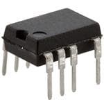
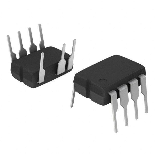
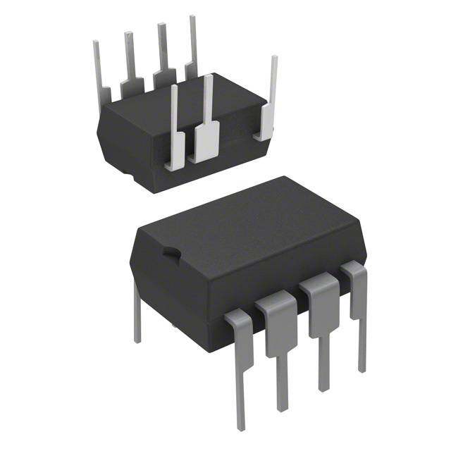
| 描述 | IC OFFLINE SWIT PROG OVP 10CSDIP交流/直流转换器 Off-Line Switcher IC 35W/92W PK |
| 产品分类 | |
| 品牌 | Power Integrations |
| 产品手册 | |
| 产品图片 |
|
| rohs | 符合RoHS无铅 / 符合限制有害物质指令(RoHS)规范要求 |
| 产品系列 | 电源管理 IC,交流/直流转换器,Power Integrations TOP258MNTOPSwitch®-HX |
| 数据手册 | |
| 产品型号 | TOP258MN |
| PCN组件/产地 | |
| 产品培训模块 | http://www.digikey.cn/PTM/IndividualPTM.page?site=cn&lang=zhs&ptm=1022 |
| 产品目录页面 | |
| 产品种类 | 交流/直流转换器 |
| 供应商器件封装 | SDIP-10C |
| 其它名称 | 596-1191-5 |
| 功率(W) | 140W |
| 包装 | 管件 |
| 占空比-最大 | 78 % |
| 商标 | Power Integrations |
| 安装风格 | SMD/SMT |
| 封装 | Tube |
| 封装/外壳 | 10-SDIP(0.300",7.62mm),9 引线 |
| 封装/箱体 | SMD-8C |
| 工作温度 | -40°C ~ 150°C |
| 工作温度范围 | - 40 C to + 150 C |
| 工厂包装数量 | 50 |
| 开关频率 | 132 kHz |
| 标准包装 | 50 |
| 电压-击穿 | 700V |
| 电压-输入 | - |
| 电压-输出 | - |
| 类型 | Off Line Switcher |
| 输入/电源电压—最大值 | 9 V |
| 输入/电源电压—最小值 | - 0.3 V |
| 输出功率 | 48 W |
| 输出电压 | 700 V |
| 输出电流 | 6.88 A |
| 输出隔离 | 隔离 |
| 配用 | /product-detail/zh/RDK-142/596-1193-ND/1657677 |
| 频率范围 | 119kHz ~ 145kHz |


- 商务部:美国ITC正式对集成电路等产品启动337调查
- 曝三星4nm工艺存在良率问题 高通将骁龙8 Gen1或转产台积电
- 太阳诱电将投资9.5亿元在常州建新厂生产MLCC 预计2023年完工
- 英特尔发布欧洲新工厂建设计划 深化IDM 2.0 战略
- 台积电先进制程称霸业界 有大客户加持明年业绩稳了
- 达到5530亿美元!SIA预计今年全球半导体销售额将创下新高
- 英特尔拟将自动驾驶子公司Mobileye上市 估值或超500亿美元
- 三星加码芯片和SET,合并消费电子和移动部门,撤换高东真等 CEO
- 三星电子宣布重大人事变动 还合并消费电子和移动部门
- 海关总署:前11个月进口集成电路产品价值2.52万亿元 增长14.8%


PDF Datasheet 数据手册内容提取
TOP252-262 TOPSwitch™-HX Family Enhanced EcoSmart™, Integrated Off-Line Switcher with Advanced Feature Set and Extended Power Range Product Highlights Lower System Cost, Higher Design Flexibility + AC DC • Multi-mode operation maximizes efficiency at all loads IN OUT - • New eSIP-7F and eSIP-7C packages • Low thermal impedance junction-to-case (2 °C per watt) • Low height is ideal for adapters where space is limited • Simple mounting using a clip to aid low cost manufacturing D V • Horizontal eSIP-7F package ideal for ultra low height adapter CONTROL and monitor applications TOPSwitch-HX C • Extended package creepage distance from DRAIN pin to S X F adjacent pin and to heat sink • No heat sink required up to 35 W using P, G and M packages with universal input voltage and up to 48 W at 230 VAC PI-4510-100206 • Output overvoltage protection (OVP) is user programmable for Figure 1. Typical Flyback Application. latching/non-latching shutdown with fast AC reset • Allows both primary and secondary sensing • Heat sink is connected to SOURCE for low EMI • Line undervoltage (UV) detection prevents turn-off glitches • Improved auto-restart delivers <3% of maximum power in • Line overvoltage (OV) shutdown extends line surge limit short circuit and open loop fault conditions • Accurate programmable current limit • Accurate hysteretic thermal shutdown function automatically • Optimized line feed-forward for line ripple rejection recovers without requiring a reset • 132 kHz frequency (254Y-258Y and all E/L packages) reduces • Fully integrated soft-start for minimum start-up stress transformer and power supply size • Extended creepage between DRAIN and all other pins • Half frequency option for video applications improves field reliability • Frequency jittering reduces EMI filter cost Output Power Table 230 VAC ±15%4 85-265 VAC 230 VAC ±15% 85-265 VAC Product5 Open Open Product5 Open Open Adapter1 Peak3 Adapter1 Peak3 Adapter1 Adapter1 Frame2 Frame2 Frame2 Frame2 TOP252PN/GN 21 W 13 W TOP252EN/EG 10 W 21 W 6 W 13 W 9 W 15 W 6 W 10 W TOP253EN/EG 21 W 43 W 13 W 29 W TOP252MN 21 W 13 W TOP254EN/YN/EG 30 W 62 W 20 W 43 W TOP253PN/GN 38 W 25 W TOP255EN/YN/EG 40 W 81 W 26 W 57 W 15 W 25 W 9 W 15 W TOP255LN 40 W 81 W 26 W 57 W TOP253MN 43 W 29 W TOP256EN/YN/EG 60 W 119 W 40 W 86 W TOP254PN/GN 47 W 30 W TOP256LN 60 W 88 W 40 W 64 W 16 W 28 W 11 W 20 W TOP254MN 62 W 40 W TOP257EN/YN/EG 85 W 157 W 55 W 119 W TOP257LN 85 W 105 W 55 W 78 W TOP255PN/GN 54 W 35 W 19 W 30 W 13 W 22 W TOP258EN/YN/EG 105 W 195 W 70 W 148 W TOP255MN 81 W 52 W TOP258LN 105 W 122 W 70 W 92 W TOP256PN/GN 63 W 40 W TOP259EN/YN/EG 128 W 238 W 80 W 171 W 21 W 34 W 15 W 26 W TOP259LN 128 W 162 W 80 W 120 W TOP256MN 98 W 64 W TOP260EN/YN/EG 147 W 275 W 93 W 200 W TOP257PN/GN 70 W 45 W TOP260LN 147 W 190 W 93 W 140 W 25 W 41 W 19 W 30 W TOP257MN 119 W 78 W TOP261EN/YN/EG 177 W 333 W 118 W 254 W TOP261LN 177 W 244 W 118 W 177 W TOP258PN/GN 77 W 50 W 29 W 48 W 22 W 35 W TOP262EN6 177 W 333 W 118 W 254 W TOP258MN 140 W 92 W TOP262LN6 177 W 244 W 118 W 177 W Table 1. Output Power Table. (for notes see page 2). www.powerint.com June 2013
TOP252-262 EcoSmart™– Energy Efficient Y Package Option for TOP259-261 • Energy efficient over entire load range In order to improve noise-immunity on large TOPSwitch-HX • No-load consumption Y package parts, the F pin has been removed (TOP259-261YN • Less than 200 mW at 230 VAC are fixed at 66 kHz switching frequency) and replaced with a • Standby power for 1 W input SIGNAL GROUND (G) pin. This pin acts as a low noise path for • >600 mW output at 110 VAC input the C pin capacitor and the X pin resistor. It is only required for • >500 mW output at 265 VAC input the TOP259-261YN package parts. Description TOPSwitch-HX cost effectively incorporates a 700 V power + MOSFET, high voltage switched current source, PWM control, AC DC oscillator, thermal shutdown circuit, fault protection and other IN OUT - control circuitry onto a monolithic device. Notes for Table 1: D V 1. Minimum continuous power in a typical non-ventilated CONTROL enclosed adapter measured at +50 °C ambient. Use of an TOPSwitch-HX C external heat sink will increase power capability. 2. Minimum continuous power in an open frame design at S X G +50 °C ambient. 3. Peak power capability in any design at +50 °C ambient. 4. 230 VAC or 110/115 VAC with doubler. PI-4973-122607 5. Packages: P: DIP-8C, G: SMD-8C, M: SDIP-10C, Figure 2. Typical Flyback Application TOP259YN, TOP260YN and TOP261YN. Y: TO-220-7C, E: eSIP-7C, L: eSIP-7F. See part ordering information. 6. TOP261 and TOP262 have the same current limit set point. In some applications TOP262 may run cooler than TOP261 due to a lower R for the larger device. DS(ON) 2 Rev. H 06/13 www.powerint.com
TOP252-262 Section List Functional Block Diagram ....................................................................................................................................... 4 Pin Functional Description ...................................................................................................................................... 6 TOPSwitch-HX Family Functional Description .......................................................................................................7 CONTROL (C) Pin Operation ....................................................................................................................................8 Oscillator and Switching Frequency ..........................................................................................................................8 Pulse Width Modulator ............................................................................................................................................9 Maximum Load Cycle ..............................................................................................................................................9 Error Amplifier ..........................................................................................................................................................9 On-Chip Current Limit with External Programmability ...............................................................................................9 Line Undervoltage Detection (UV) ...........................................................................................................................10 Line Overvoltage Shutdown (OV) ............................................................................................................................11 Hysteretic or Latching Output Overvoltage Protection (OVP)...................................................................................11 Line Feed-Forward with DC Reduction ..............................................................................................................13 MAX Remote ON/OFF and Synchronization ....................................................................................................................13 Soft-Start ...............................................................................................................................................................13 Shutdown/Auto-Restart .........................................................................................................................................13 Hysteretic Over-Temperature Protection .................................................................................................................13 Bandgap Reference ...............................................................................................................................................13 High-Voltage Bias Current Source ..........................................................................................................................13 Typical Uses of FREQUENCY (F) Pin ......................................................................................................................15 Typical Uses of VOLTAGE MONITOR (V) and EXTERNAL CURRENT LIMIT (X) Pins ..........................................16 Typical Uses of MULTI-FUNCTION (M) Pin ...........................................................................................................18 Application Examples ..............................................................................................................................................21 A High Efficiency, 35 W, Dual Output – Universal Input Power Supply .....................................................................21 A High Efficiency, 150 W, 250-380 VDC Input Power Supply ..................................................................................22 A High Efficiency, 20 W Continuous – 80 W Peak, Universal Input Power Supply ...................................................23 A High Efficiency, 65 W, Universal Input Power Supply ...........................................................................................24 Key Application Considerations ..............................................................................................................................25 TOPSwitch-HX vs.TOPSwitch-GX ........................................................................................................................ 25 TOPSwitch-HX Design Considerations ..................................................................................................................26 TOPSwitch-HX Layout Considerations ...................................................................................................................27 Quick Design Checklist ..........................................................................................................................................31 Design Tools ..........................................................................................................................................................31 Product Specifications and Test Conditions ..........................................................................................................32 Typical Performance Characteristics ....................................................................................................................39 Package Outlines ....................................................................................................................................................43 Part Ordering Information ........................................................................................................................................47 3 www.powerint.com Rev. H 06/13
TOP252-262 VC 0 CONTROL (C) DRAIN (D) ZC INTERNAL 1 SUPPLY SHUNT REGULATOR/ - ERROR AMPLIFIER + + - 54..88 VV - SOFT START + 5.8 V IFB CINOTMEPRANRAALT UOVR KPS(UPPER) - + CURRENT VI (LIMIT) LIMIT AD JUST √ 16 KPS(LOWER) - ON/OFF + SHUTDOWN/ AUTO-RESTART CURRENT LIMIT VBG + VT COMPARATOR FUNMCUTLIOTNI- (M) STOP LOGIC HYTHSTEERRMEATLI C SOURCE (S) SHUTDOWN CONTROLLED TURN-ON STOP SOFT GATE DRIVER V OVP OV/ START UV SLEINNSEE DCMAX DCMAX OWSITCHIL JLIATTTOERR CLDOMCAKX F REDUCTION S Q LEADING R EDGE BLANKING F REDUCTION SOFT START IFB PWM OFF KPS(UPPER) IPS(UPPER) KPS(LOWER) IPS(LOWER) SOURCE (S) PI-4508-120307 Figure 3a. Functional Block Diagram (P and G Packages). VC 0 CONTROL (C) DRAIN (D) ZC INTERNAL 1 SUPPLY SHUNT REGULATOR/ - ERROR AMPLIFIER + + - 54..88 VV - SOFT START + 5.8 V IFB CINOTMEPRANRAALT UOVR KPS(UPPER) - + CURRENT VI (LIMIT) LIMIT AD JUST √ 16 KPS(LOWER) - ON/OFF + SHUTDOWN/ EXTERNAL AUTO-RESTART CURRENT LIMIT CLUIMRIRTE (NX)T VBG + VT COMPARATOR VOLTAGE STOP LOGIC HYSTERETIC MONITOR (V) THERMAL SOURCE (S) 1 V SHUTDOWN CONTROLLED TURN-ON STOP SOFT GATE DRIVER V OVP OV/ START SLEINNSEE DCMUAVX DCMAX OWSITCHIL JLIATTTOERR CLDOMCAKX F REDUCTION S Q LEADING R EDGE BLANKING F REDUCTION SOFT START IFB PWM OFF KPS(UPPER) IPS(UPPER) KPS(LOWER) IPS(LOWER) SOURCE (S) PI-4643-082907 Figure 3b. Functional Block Diagram (M Package). 4 Rev. H 06/13 www.powerint.com
TOP252-262 VC 0 CONTROL (C) DRAIN (D) ZC INTERNAL 1 SUPPLY SHUNT REGULATOR/ - ERROR AMPLIFIER + + - 54..88 VV - SOFT START + 5.8 V IFB CINOTMEPRANRAALT UOVR KPS(UPPER) - + CURRENT VI (LIMIT) LIMIT AD JUST √ 16 KPS(LOWER) - ON/OFF + SHUTDOWN/ EXTERNAL AUTO-RESTART CURRENT LIMIT CLUIMRIRTE (NX)T VBG + VT COMPARATOR VOLTAGE STOP LOGIC HYSTERETIC MONITOR (V) THERMAL SOURCE (S) 1 V SHUTDOWN CONTROLLED TURN-ON STOP SOFT GATE DRIVER V OVP OV/ START SLEINNSEE DCMUAVX D CMAX OWSITCHIL JLIATTTOERR CLDOMCAKX 66k/132k F REDUCTION S Q LEADING R EDGE FREQUENCY BLANKING (F) F REDUCTION SOFT START IFB PWM OFF KPS(UPPER) IPS(UPPER) KPS(LOWER) IPS(LOWER) SOURCE (S) PI-4511-082907 Figure 3c. Functional Block Diagram (TOP254-258 YN Package and all eSIP Packages). VC 0 CONTROL (C) DRAIN (D) ZC INTERNAL 1 SUPPLY SHUNT REGULATOR/ - ERROR AMPLIFIER + + - 54..88 VV - SOFT START + 5.8 V IFB CINOTMEPRANRAALT UOVR KPS(UPPER) - + CURRENT VI (LIMIT) LIMIT AD JUST √ 16 KPS(LOWER) - ON/OFF + SHUTDOWN/ EXTERNAL AUTO-RESTART CURRENT LIMIT CLUIMRIRTE (NX)T VBG + VT COMPARATOR VOLTAGE STOP LOGIC HYSTERETIC MONITOR (V) THERMAL SOURCE (S) 1 V SHUTDOWN CONTROLLED TURN-ON STOP SOFT GATE DRIVER V OVP OV/ START SLEINNSEE DCMUAVX DCMAX OWSITCHIL JLIATTTOERR CLDOMCAKX F REDUCTION S Q LEADING R EDGE SOURCE (S) BLANKING F REDUCTION SOFT START IFB PWM OFF KPS(UPPER) IPS(UPPER) KPS(LOWER) IPS(LOWER) SIGNAL PI-4974-122607 GROUND (G) Figure 3d. Functional Block Diagram TOP259YN, TOP260YN, TOP261YN. 5 www.powerint.com Rev. H 06/13
TOP252-262 Pin Functional Description VOLTAGE MONITOR (V) Pin (Y & M package only): Input for OV, UV, line feed forward with DC reduction, output DRAIN (D) Pin: MAX overvoltage protection (OVP), remote ON/OFF and device reset. High-voltage power MOSFET DRAIN pin. The internal start-up A connection to the SOURCE pin disables all functions on this pin. bias current is drawn from this pin through a switched high- voltage current source. Internal current limit sense point for MULTI-FUNCTION (M) Pin (P & G packages only): drain current. This pin combines the functions of the VOLTAGE MONITOR (V) and EXTERNAL CURRENT LIMIT (X) pins of the Y package into CONTROL (C) Pin: one pin. Input pin for OV, UV, line feed forward with DC Error amplifier and feedback current input pin for duty cycle MAX control. Internal shunt regulator connection to provide internal 8 0 bias current during normal operation. It is also used as the 13 ccoomnnpeecntisoant iopno incta pfoarc tihtoer .supply bypass and auto-restart/ + R 4 MΩ V VFUOoVVr ==R LIIUOSV V= ×× 4 RR MLLSSΩ ++ VVVV ((IIVV == IIUOVV)) PI-4711-02 EXTERNAL CURRENT LIMIT (X) Pin (Y, M, E and L package): LS VUV = 102.8 VDC V = 451 VDC Input pin for external current limit adjustment and remote OV ON/OFF. A connection to SOURCE pin disables all functions on InDpCut D V DDCCMAX@@130705 VVDDCC == 7461%% this pin. Voltage CONTROL MAX C For R = 12 kΩ IL I = 61% S X LIMIT E Package (eSIP-7C) Y Package (TO-220-7C) R See Figure 55b for Note: Y package for TOP259-261 - 12IL kΩ other resistor values (R ) to select different Exposed Pad IL I values. (Hidden) LIMIT Internally Connected to Figure 5. TOP254-258 Y and All M/E/L Package Line Sense and Externally Set SOURCE Pin Current Limit. 8 0 3 1 L PaV1cXk2aC3geF4 (S5eSID7P-7F) TCSaOobnU nIRnetCceEtren dPa iltnloy + R 4 MΩ V VFUOoVVr ==R LIIUOSV V= ×× 4 RR MLLSSΩ ++ VVVV ((IIVV == IIUOVV)) PI-4983-02 LS V = 102.8 VDC UV V = 451 VDC OV DC DCMAX@100 VDC = 76% Input D V DC @375 VDC = 41% 12345 7 MAX VXCSG D Voltage CONTROL C Lead Bend Outward from Drawing For RIL = 12 kΩ (Refer to eSIP-7F Package S X G ILIMIT = 61% 12345 7 Outline Drawing) VXCFS D See Figure 55b for R M Package Y Package (TO-220-7C) - 12IL kΩ o(Rthe)r t ore sseisletocrt vdaiflfueeres nt IL Note: Y package for TOP254-258 ILIMIT values. V 1 10 S X 2 9 S Figure 6. TOP259-261 Y Package Line Sense and External Current Limit. C 3 8 S 7 S + D 5 6 S VUV = IUV × RLS + VM (IM = IUV) VOV = IOV × RLS + VM (IM = IOV) Tab Internally P and G Package CSOonUnReCcEte dP itno RLS 4 MΩ F o r VRULVS == 140 M2.Ω8 VDC M 1 8 S DC VOV = 451 VDC Input DC @100 VDC = 76% C 2 7 S Voltage DCMAX@375 VDC = 41% MAX D M 6 S 12345 7 CONTROL VXCSF D C D 4 5 S PI-4644-091108 - S Figure 4. Pin Configuration (Top View). PI-4712-120307 Figure 7. P/G Package Line Sense. 6 Rev. H 06/13 www.powerint.com
TOP252-262 Auto-Restart + 78 F oIr RIL == 6112% k Ω Slope = PWM Gain LIMIT (constant over load range) %) F oILr IMRIITL == 3179% k Ω cle ( y DC C Input See Figure 55b for other y Voltage sreesleisctto dr ivffaelrueenst (IRIL) tvoa lues. Dut LIMIT D M CONTROL RIL C CONTROL Current - S PI-4713-021308 %) 100 Figure 8. P/G Package Externally Set Current Limit. nt o ( urreRati reduction, output overvoltage protection (OVP), external current k Cmit 55 lcimonitn aedcjtuiosntm toe nSt,O rUemRCotEe pOinN d/OisFaFb laensd a dll efuvniccet iorensse ot.n Ath is pin n Peaent Li and makes TOPSwitch-HX operate in simple three terminal DraiCurr mode (like TOPSwitch-II). o 25 T FREQUENCY (F) Pin (TOP254-258Y, and all E and L packages): CONTROL Input pin for selecting switching frequency 132 kHz if connected Current to SOURCE pin and 66 kHz if connected to CONTROL pin. Full Frequency Mode The switching frequency is internally set for fixed 66 kHz 132 operation in the P, G, M package and TOP259YN, TOP260YN Low and TOP261YN. kHz) FVreaqriuaebnlec y FreMqoudeen cy SIGNAL GROUND (G) Pin (TOP259YN, TOP260YN & y ( 66 Mode c n TOP261YN only): ue Jitter Multi-Cycle Return for C pin capacitor and X pin resistor. eq Modulation Fr SOURCE (S) Pin: 30 Output MOSFET source connection for high voltage power return. Primary side control circuit common and reference point. I I I I I I CONTROL CD1 B C01 C02 C03 COFF Current PI-4645-041107 TOPSwitch-HX Family Functional Description Figure 9. Control Pin Characteristics (Multi-Mode Operation). Like TOPSwitch-GX, TOPSwitch-HX is an integrated switched two terminals, VOLTAGE-MONITOR and EXTERNAL CURRENT mode power supply chip that converts a current at the control LIMIT (available in M package) or one terminal MULTI-FUNCTION input to a duty cycle at the open drain output of a high voltage (available in P and G package) have been used to implement power MOSFET. During normal operation the duty cycle of the some of the new functions. These terminals can be connected power MOSFET decreases linearly with increasing CONTROL to the SOURCE pin to operate the TOPSwitch-HX in a pin current as shown in Figure 9. TOPSwitch-like three terminal mode. However, even in this three terminal mode, the TOPSwitch-HX offers many transparent In addition to the three terminal TOPSwitch features, such as features that do not require any external components: the high voltage start-up, the cycle-by-cycle current limiting, loop compensation circuitry, auto-restart and thermal 1. A fully integrated 17 ms soft-start significantly reduces or shutdown, the TOPSwitch-HX incorporates many additional eliminates output overshoot in most applications by sweeping functions that reduce system cost, increase power supply both current limit and frequency from low to high to limit the performance and design flexibility. A patented high voltage peak currents and voltages during start-up. CMOS technology allows both the high-voltage power MOSFET 2. A maximum duty cycle (DC ) of 78% allows smaller input MAX and all the low voltage control circuitry to be cost effectively storage capacitor, lower input voltage requirement and/or integrated onto a single monolithic chip. higher power capability. 3. Multi-mode operation optimizes and improves the power Three terminals, FREQUENCY, VOLTAGE-MONITOR, and supply efficiency over the entire load range while maintaining EXTERNAL CURRENT LIMIT (available in Y and E/L packages), good cross regulation in multi-output supplies. 7 www.powerint.com Rev. H 06/13
TOP252-262 4. Switching frequency of 132 kHz reduces the transformer size current source connected internally between the DRAIN and with no noticeable impact on EMI. CONTROL pins. When the CONTROL pin voltage V reaches C 5. Frequency jittering reduces EMI in the full frequency mode at approximately 5.8 V, the control circuitry is activated and the high load condition. soft-start begins. The soft-start circuit gradually increases the 6. Hysteretic over-temperature shutdown ensures automatic drain peak current and switching frequency from a low starting recovery from thermal fault. Large hysteresis prevents circuit value to the maximum drain peak current at the full frequency board overheating. over approximately 17 ms. If no external feedback/supply 7. Packages with omitted pins and lead forming provide large current is fed into the CONTROL pin by the end of the soft-start, drain creepage distance. the high voltage current source is turned off and the CONTROL 8. Reduction of the auto-restart duty cycle and frequency to pin will start discharging in response to the supply current improve the protection of the power supply and load during drawn by the control circuitry. If the power supply is designed open loop fault, short circuit, or loss of regulation. properly, and no fault condition such as open loop or shorted 9. Tighter tolerances on I2f power coefficient, current limit output exists, the feedback loop will close, providing external reduction, PWM gain and thermal shutdown threshold. CONTROL pin current, before the CONTROL pin voltage has had a chance to discharge to the lower threshold voltage of The VOLTAGE-MONITOR (V) pin is usually used for line sensing approximately 4.8 V (internal supply undervoltage lockout by connecting a 4 MW resistor from this pin to the rectified DC threshold). When the externally fed current charges the high voltage bus to implement line overvoltage (OV), under- CONTROL pin to the shunt regulator voltage of 5.8 V, current in voltage (UV) and dual-slope line feed-forward with DC excess of the consumption of the chip is shunted to SOURCE MAX reduction. In this mode, the value of the resistor determines the through an NMOS current mirror as shown in Figure 3. The OV/UV thresholds and the DC is reduced linearly with a dual output current of that NMOS current mirror controls the duty MAX slope to improve line ripple rejection. In addition, it also cycle of the power MOSFET to provide closed loop regulation. provides another threshold to implement the latched and The shunt regulator has a finite low output impedance Z that C hysteretic output overvoltage protection (OVP). The pin can sets the gain of the error amplifier when used in a primary also be used as a remote ON/OFF using the I threshold. feedback configuration. The dynamic impedance Z of the UV C CONTROL pin together with the external CONTROL pin The EXTERNAL CURRENT LIMIT (X) pin can be used to reduce capacitance sets the dominant pole for the control loop. the current limit externally to a value close to the operating peak current, by connecting the pin to SOURCE through a resistor. When a fault condition such as an open loop or shorted output This pin can also be used as a remote ON/OFF input. prevents the flow of an external current into the CONTROL pin, the capacitor on the CONTROL pin discharges towards 4.8 V. For the P and G package the VOLTAGE-MONITOR and At 4.8 V, auto-restart is activated, which turns the output EXTERNAL CURRENT LIMIT pin functions are combined on MOSFET off and puts the control circuitry in a low current one MULTI-FUNCTION (M) pin. However, some of the functions standby mode. The high-voltage current source turns on and become mutually exclusive. charges the external capacitance again. A hysteretic internal supply undervoltage comparator keeps V within a window of C The FREQUENCY (F) pin in the TOP254-258 Y and E/L packages typically 4.8 V to 5.8 V by turning the high-voltage current set the switching frequency in the full frequency PWM mode to source on and off as shown in Figure 11. The auto-restart the default value of 132 kHz when connected to SOURCE pin. A circuit has a divide-by-sixteen counter, which prevents the half frequency option of 66 kHz can be chosen by connecting output MOSFET from turning on again until sixteen discharge/ this pin to the CONTROL pin instead. Leaving this pin open is charge cycles have elapsed. This is accomplished by enabling not recommended. In the P, G and M packages and the the output MOSFET only when the divide-by-sixteen counter TOP259-261 Y packages, the frequency is set internally at reaches the full count (S15). The counter effectively limits 66 kHz in the full frequency PWM mode. TOPSwitch-HX power dissipation by reducing the auto-restart duty cycle to typically 2%. Auto-restart mode continues until CONTROL (C) Pin Operation output voltage regulation is again achieved through closure of The CONTROL pin is a low impedance node that is capable of the feedback loop. receiving a combined supply and feedback current. During normal operation, a shunt regulator is used to separate the Oscillator and Switching Frequency feedback signal from the supply current. CONTROL pin voltage The internal oscillator linearly charges and discharges an V is the supply voltage for the control circuitry including the internal capacitance between two voltage levels to create a C MOSFET gate driver. An external bypass capacitor closely triangular waveform for the timing of the pulse width modulator. connected between the CONTROL and SOURCE pins is This oscillator sets the pulse width modulator/current limit latch required to supply the instantaneous gate drive current. The at the beginning of each cycle. total amount of capacitance connected to this pin also sets the auto-restart timing as well as control loop compensation. The nominal full switching frequency of 132 kHz was chosen to When rectified DC high voltage is applied to the DRAIN pin minimize transformer size while keeping the fundamental EMI during start-up, the MOSFET is initially off, and the CONTROL frequency below 150 kHz. The FREQUENCY pin (available only pin capacitor is charged through a switched high voltage in TOP254-258 Y and E, L packages), when shorted to the CONTROL pin, lowers the full switching frequency to 66 kHz 8 Rev. H 06/13 www.powerint.com
TOP252-262 FSrweqit ucehnincgy fOSC + PI-4530-041107 profaepamdceukirlcaiaettgsiioo.e nns T )oi.sO f DiPtdhSueetwn yot iitcnccy-ahtcli- mltHeo eX ist hw oreenh dPleyunW oc IpMeC edi src a foirntoencmstrr eo iDnal sCothefM idasA Xl lbm toehotyrhdooeeunr gd iTfh OItB ht.Ph e Se T whiistc h fOSC - cycle-by-cycle peak drain current stays above k *I (set), PS(UPPER) LIMIT where k is 55% (typical) and I (set) is the current limit PS(UPPER) LIMIT externally set via the X or M pin. 4 ms Variable Frequency PWM mode: When peak drain current is VDRAIN lowered to k * I (set) as a result of power supply load PS(UPPER) LIMIT reduction, the PWM modulator initiates the transition to variable Time frequency PWM mode, and gradually turns off frequency jitter. In this mode, peak drain current is held constant at k * PS(UPPER) Figure 10. Switching Frequency Jitter (Idealized V Waveforms). I (set) while switching frequency drops from the initial full DRAIN LIMIT frequency of f (132 kHz or 66 kHz) towards the minimum OSC (half frequency), which may be preferable in some cases such frequency of f (30 kHz typical). Duty cycle reduction is MCM(MIN) as noise sensitive video applications or a high efficiency accomplished by extending the off-time. standby mode. Otherwise, the FREQUENCY pin should be connected to the SOURCE pin for the default 132 kHz. In the Low Frequency PWM mode: When switching frequency M, P and G packages and the TOP259-261 Y package option, reaches f (30 kHz typical), the PWM modulator starts to MCM(MIN) the full frequency PWM mode is set at 66 kHz, for higher transition to low frequency mode. In this mode, switching efficiency and increased output power in all applications. frequency is held constant at f and duty cycle is reduced, MCM(MIN) similar to the full frequency PWM mode, through the reduction To further reduce the EMI level, the switching frequency in the of the on-time. Peak drain current decreases from the initial full frequency PWM mode is jittered (frequency modulated) by value of k * I (set) towards the minimum value of PS(UPPER) LIMIT approximately ±2.5 kHz for 66 kHz operation or ±5 kHz for k *I (set), where k is 25% (typical) and I (set) is PS(LOWER) LIMIT PS(LOWER) LIMIT 132 kHz operation at a 250 Hz (typical) rate as shown in the current limit externally set via the X or M pin. Figure 10. The jitter is turned off gradually as the system is entering the variable frequency mode with a fixed peak drain Multi-Cycle-Modulation mode: When peak drain current is current. lowered to k *I (set), the modulator transitions to PS(LOWER) LIMIT multi-cycle-modulation mode. In this mode, at each turn-on, Pulse Width Modulator the modulator enables output switching for a period of T MCM(MIN) The pulse width modulator implements multi-mode control by at the switching frequency of f (4 or 5 consecutive pulses MCM(MIN) driving the output MOSFET with a duty cycle inversely at 30 kHz) with the peak drain current of k *I (set), and PS(LOWER) LIMIT proportional to the current into the CONTROL pin that is in stays off until the CONTROL pin current falls below I . This C(OFF) excess of the internal supply current of the chip (see Figure 9). mode of operation not only keeps peak drain current low but The feedback error signal, in the form of the excess current, is also minimizes harmonic frequencies between 6 kHz and filtered by an RC network with a typical corner frequency of 30 kHz. By avoiding transformer resonant frequency this way, 7 kHz to reduce the effect of switching noise in the chip supply all potential transformer audible noises are greatly suppressed. current generated by the MOSFET gate driver. Maximum Duty Cycle To optimize power supply efficiency, four different control The maximum duty cycle, DC , is set at a default maximum MAX modes are implemented. At maximum load, the modulator value of 78% (typical). However, by connecting the VOLTAGE- operates in full frequency PWM mode; as load decreases, the MONITOR or MULTI-FUNCTION pin (depending on the modulator automatically transitions, first to variable frequency package) to the rectified DC high voltage bus through a resistor PWM mode, then to low frequency PWM mode. At light load, with appropriate value (4 MW typical), the maximum duty cycle the control operation switches from PWM control to multi-cycle- can be made to decrease from 78% to 40% (typical) when input modulation control, and the modulator operates in multi-cycle- line voltage increases from 88 V to 380 V, with dual gain slopes. modulation mode. Although different modes operate differently Error Amplifier to make transitions between modes smooth, the simple The shunt regulator can also perform the function of an error relationship between duty cycle and excess CONTROL pin amplifier in primary side feedback applications. The shunt current shown in Figure 9 is maintained through all three PWM regulator voltage is accurately derived from a temperature- modes. Please see the following sections for the details of the compensated bandgap reference. The CONTROL pin dynamic operation of each mode and the transitions between modes. impedance Z sets the gain of the error amplifier. The C CONTROL pin clamps external circuit signals to the V voltage Full Frequency PWM mode: The PWM modulator enters full C level. The CONTROL pin current in excess of the supply current frequency PWM mode when the CONTROL pin current (I ) C is separated by the shunt regulator and becomes the feedback reaches I . In this mode, the average switching frequency is B current I for the pulse width modulator. kept constant at f (66 kHz for P, G and M packages and fb OSC TOP259-261 Y, pin selectable 132 kHz or 66 kHz for Y and E/L 9 www.powerint.com Rev. H 06/13
TOP252-262 ~~ ~~ V UV ~ ~ ~ ~ ~ ~ V LINE 0 V S15 S14 S13 ~ S~ 12 S0 S15 S14 S13 S~ ~ 12 S0 S15 S14 S13 ~ S~ 12 S0 S15 S15 5.8 V V 4.8 V C 0 V ~ ~ ~ ~ V DRAIN ~~ 0 V V OUT 0 V ~~ ~~ ~~ 1 2 3 2 4 Note: S0 through S15 are the output states of the auto-restart counter PI-4531-121206 Figure 11. Typical Waveforms for (1) Power Up (2) Normal Operation (3) Auto-Restart (4) Power Down. On-Chip Current Limit with External Programmability on. The leading edge blanking time has been set so that, if a The cycle-by-cycle peak drain current limit circuit uses the power supply is designed properly, current spikes caused by output MOSFET ON-resistance as a sense resistor. A current primary-side capacitances and secondary-side rectifier reverse limit comparator compares the output MOSFET on-state drain recovery time should not cause premature termination of the to source voltage V with a threshold voltage. High drain switching pulse. DS(ON) current causes V to exceed the threshold voltage and turns DS(ON) the output MOSFET off until the start of the next clock cycle. The current limit is lower for a short period after the leading The current limit comparator threshold voltage is temperature edge blanking time. This is due to dynamic characteristics of compensated to minimize the variation of the current limit due the MOSFET. During startup and fault conditions the controller to temperature related changes in R of the output MOSFET. prevents excessive drain currents by reducing the switching DS(ON) The default current limit of TOPSwitch-HX is preset internally. frequency. However, with a resistor connected between EXTERNAL CURRENT LIMIT (X) pin (Y, E/L and M packages) or MULTI- Line Undervoltage Detection (UV) FUNCTION (M) pin (P and G package) and SOURCE pin (for At power up, UV keeps TOPSwitch-HX off until the input line TOP259-261 Y, the X pin is connected to the SIGNAL GROUND voltage reaches the undervoltage threshold. At power down, (G) pin), current limit can be programmed externally to a lower UV prevents auto-restart attempts after the output goes out of level between 30% and 100% of the default current limit. By regulation. This eliminates power down glitches caused by slow setting current limit low, a larger TOPSwitch-HX than necessary discharge of the large input storage capacitor present in for the power required can be used to take advantage of the applications such as standby supplies. A single resistor lower R for higher efficiency/smaller heat sinking connected from the VOLTAGE-MONITOR pin (Y, E/L and M DS(ON) requirements. TOPSwitch-HX current limit reduction initial packages) or MULTI-FUNCTION pin (P and G packages) to the tolerance through the X pin (or M pin) has been improved rectified DC high voltage bus sets UV threshold during power significantly compare with previous TOPSwitch-GX. With a up. Once the power supply is successfully turned on, the UV second resistor connected between the EXTERNAL CURRENT threshold is lowered to 44% of the initial UV threshold to allow LIMIT (X) pin (Y, E/L and M packages) or MULTI-FUNCTION (M) extended input voltage operating range (UV low threshold). If pin (P and G package) and the rectified DC high voltage bus, the UV low threshold is reached during operation without the the current limit is reduced with increasing line voltage, allowing power supply losing regulation, the device will turn off and stay a true power limiting operation against line variation to be off until UV (high threshold) has been reached again. If the implemented. When using an RCD clamp, this power limiting power supply loses regulation before reaching the UV low technique reduces maximum clamp voltage at high line. This threshold, the device will enter auto-restart. At the end of each allows for higher reflected voltage designs as well as reducing auto-restart cycle (S15), the UV comparator is enabled. If the clamp dissipation. UV high threshold is not exceeded, the MOSFET will be disabled during the next cycle (see Figure 11). The UV feature The leading edge blanking circuit inhibits the current limit can be disabled independent of the OV feature. comparator for a short time after the output MOSFET is turned 10 Rev. H 06/13 www.powerint.com
TOP252-262 Line Overvoltage Shutdown (OV) clamp network, bias winding return or power traces from other The same resistor used for UV also sets an overvoltage converters. If the line sensing features are used, then the sense threshold, which, once exceeded, will force TOPSwitch-HX to resistors must be placed within 10 mm of the V-pin to minimize stop switching instantaneously (after completion of the current the V-pin node area. The DC bus should then be routed to the switching cycle). If this condition lasts for at least 100 ms, the line sense resistors. Note that external capacitance must not TOPSwitch-HX output will be forced into off state. Unlike with be connected to the V-pin as this may cause misoperation of TOPSwitch-GX, however, when the line voltage is back to the V pin related functions. normal with a small amount of hysteresis provided on the OV threshold to prevent noise triggering, the state machine sets to Hysteretic or Latching Output Overvoltage Protection (OVP) S13 and forces TOPSwitch-HX to go through the entire auto- The detection of the hysteretic or latching output overvoltage restart sequence before attempting to switch again. The ratio protection (OVP) is through the trigger of the line overvoltage of OV and UV thresholds is preset at 4.5, as can be seen in threshold. The V-pin or M-pin voltage will drop by 0.5 V, and Figure 12. When the MOSFET is off, the rectified DC high the controller measures the external attached impedance voltage surge capability is increased to the voltage rating of the immediately after this voltage drops. If I or I exceeds I V M OV(LS) MOSFET (700 V), due to the absence of the reflected voltage (336 mA typical) longer than 100 ms, TOPSwitch-HX will latch and leakage spikes on the drain. The OV feature can be into a permanent off state for the latching OVP. It only can be disabled independent of the UV feature. reset if V or V goes below 1 V or V goes below the power- V M C up-reset threshold (V ) and then back to normal. C(RESET) In order to reduce the no-load input power of TOPSwitch-HX designs, the V-pin (or M-pin for P Package) operates at very low If I or I does not exceed I or exceeds no longer than V M OV(LS) currents. This requires careful layout considerations when 100 ms, TOPSwitch-HX will initiate the line overvoltage and the designing the PCB to avoid noise coupling. Traces and hysteretic OVP. Their behavior will be identical to the line components connected to the V-pin should not be adjacent to overvoltage shutdown (OV) that has been described in detail in any traces carrying switching currents. These include the drain, the previous section. Voltage Monitor and External Current Limit Pin Table* Figure Number 16 17 18 19 20 21 22 23 24 25 26 27 28 Three Terminal Operation 3 Line Undervoltage 3 3 3 3 3 3 Line Overvoltage 3 3 3 3 3 3 Line Feed-Forward (DC ) 3 3 3 3 3 MAX Output Overvoltage Protection 3 3 Overload Power Limiting 3 External Current Limit 3 3 3 3 3 Remote ON/OFF 3 3 3 Device Reset 3 *This table is only a partial list of many VOLTAGE MONITOR and EXTERNAL CURRENT LIMIT Pin Configurations that are possible. Table 2. VOLTAGE MONITOR (V) Pin and EXTERNAL CURRENT LIMIT (X) Pin Configuration Options. Multi-Function Pin Table* Figure Number 29 30 31 32 33 34 35 36 37 38 39 40 Three Terminal Operation 3 Line Undervoltage 3 3 3 3 Line Overvoltage 3 3 3 3 Line Feed-Forward (DC ) 3 3 3 MAX Output Overvoltage Protection 3 3 Overload Power Limiting 3 External Current Limit 3 3 3 3 Remote ON/OFF 3 3 3 Device Reset 3 *This table is only a partial list of many MULTI-FUNCTIONAL Pin Configurations that are possible. Table 3. MULTI-FUNCTION (M) Pin Configuration Options. 11 www.powerint.com Rev. H 06/13
TOP252-262 M Pin X Pin V Pin I I I I REM(N) UV OV OV(LS) (Enabled) Output (Non-Latching) (Latching) MOSFET Switching (Disabled) Disabled when supply I output goes out of regulation I (Default) LIMIT Current Limit I DC (78%) MAX Maximum Duty Cycle I V BG Pin Voltage I -250 -200 -150 -100 -50 0 25 50 75 100 125 336 X and V Pins (Y, E, L and M Packages) and M Pin (P and G Packages) Current (µA) Note: This figure provides idealized functional characteristics with typical performance values. Please refer to the parametric table and typical performance characteristics sections of the data sheet for measured data. For a detailed description of each functional pin operation refer to the Functional Description section of the data sheet. PI-4646-071708 Figure 12. MULTI-FUNCTION (P and G package). VOLTAGE MONITOR and EXTERNAL CURRENT LIMIT (Y, E/L and M package) Pin Characteristics. The circuit examples shown in Figures 41, 42 and 43 show a The primary sensed OVP protection circuit shown in Figures 41, simple method for implementing the primary sensed over- 42 and 43 is triggered by a significant rise in output voltage (and voltage protection. therefore bias winding voltage). If the power supply is operating under heavy load or low input line conditions when an open During a fault condition resulting from loss of feedback, output loop occurs, the output voltage may not rise significantly. voltage will rapidly rise above the nominal voltage. The increase Under these conditions, a latching shutdown will not occur until in output voltage will also result in an increase in the voltage at load or line conditions change. Nevertheless, the operation the output of the bias winding. A voltage at the output of the provides the desired protection by preventing significant rise in bias winding that exceeds of the sum of the voltage rating of the the output voltage when the line or load conditions do change. Zener diode connected from the bias winding output to the Primary side OVP protection with the TOPSwitch-HX in a typical V-pin (or M-pin) and V-pin (or M-pin) voltage, will cause a current application will prevent a nominal 12 V output from rising above in excess of I or I to be injected into the V-pin approximately 20 V under open loop conditions. If greater V M (or M-pin), which will trigger the OVP feature. accuracy is required, a secondary sensed OVP circuit is recommended. 12 Rev. H 06/13 www.powerint.com
TOP252-262 Line Feed-Forward with DC Reduction Soft-Start MAX The same resistor used for UV and OV also implements line voltage The 17 ms soft-start sweeps the peak drain current and feed-forward, which minimizes output line ripple and reduces switching frequency linearly from minimum to maximum value power supply output sensitivity to line transients. Note that for the by operating through the low frequency PWM mode and the same CONTROL pin current, higher line voltage results in smaller variable frequency mode before entering the full frequency operating duty cycle. As an added feature, the maximum duty mode. In addition to start-up, soft-start is also activated at each cycle DC is also reduced from 78% (typical) at a voltage slightly restart attempt during auto-restart and when restarting after MAX lower than the UV threshold to 36% (typical) at the OV threshold. being in hysteretic regulation of CONTROL pin voltage (V ), due C DC of 36% at high line was chosen to ensure that the power to remote OFF or thermal shutdown conditions. This effectively MAX capability of the TOPSwitch-HX is not restricted by this feature minimizes current and voltage stresses on the output MOSFET, under normal operation. TOPSwitch-HX provides a better fit to the the clamp circuit and the output rectifier during start-up. This ideal feed-forward by using two reduction slopes: -1% per mA for all feature also helps minimize output overshoot and prevents bus voltage less than 195 V (typical for 4 MW line impedance) and saturation of the transformer during start-up. -0.25% per mA for all bus voltage more than 195 V. This dual Shutdown/Auto-Restart slope line feed-forward improves the line ripple rejection To minimize TOPSwitch-HX power dissipation under fault significantly compared with the TOPSwitch-GX. conditions, the shutdown/auto-restart circuit turns the power Remote ON/OFF supply on and off at an auto-restart duty cycle of typically 2% if an out of regulation condition persists. Loss of regulation TOPSwitch-HX can be turned on or off by controlling the interrupts the external current into the CONTROL pin. V current into the VOLTAGE-MONITOR pin or out from the C regulation changes from shunt mode to the hysteretic auto- EXTERNAL CURRENT LIMIT pin (Y, E/L and M packages) and restart mode as described in CONTROL pin operation section. into or out from the MULTI-FUNCTION pin (P and G package, When the fault condition is removed, the power supply output see Figure 12). In addition, the VOLTAGE-MONITOR pin has a becomes regulated, V regulation returns to shunt mode, and 1 V threshold comparator connected at its input. This voltage C threshold can also be used to perform remote ON/OFF control. normal operation of the power supply resumes. Hysteretic Over-Temperature Protection When a signal is received at the VOLTAGE-MONITOR pin or the Temperature protection is provided by a precision analog circuit EXTERNAL CURRENT LIMIT pin (Y, E/L and M packages) or the that turns the output MOSFET off when the junction temperature MULTI-FUNCTION pin (P and G package) to disable the output exceeds the thermal shutdown temperature (142 °C typical). through any of the pin functions such as OV, UV and remote When the junction temperature cools to below the lower ON/OFF, TOPSwitch-HX always completes its current switching hysteretic temperature point, normal operation resumes, thus cycle before the output is forced off. providing automatic recovery. A large hysteresis of 75 °C (typical) is provided to prevent overheating of the PC board due As seen above, the remote ON/OFF feature can also be used as to a continuous fault condition. V is regulated in hysteretic a standby or power switch to turn off the TOPSwitch-HX and C mode, and a 4.8 V to 5.8 V (typical) triangular waveform is keep it in a very low power consumption state for indefinitely present on the CONTROL pin while in thermal shutdown. long periods. If the TOPSwitch-HX is held in remote off state for long enough time to allow the CONTROL pin to discharge to the Bandgap Reference internal supply undervoltage threshold of 4.8 V (approximately All critical TOPSwitch-HX internal voltages are derived from a 32 ms for a 47 mF CONTROL pin capacitance), the CONTROL temperature-compensated bandgap reference. This voltage pin goes into the hysteretic mode of regulation. In this mode, reference is used to generate all other internal current the CONTROL pin goes through alternate charge and discharge references, which are trimmed to accurately set the switching cycles between 4.8 V and 5.8 V (see CONTROL pin operation frequency, MOSFET gate drive current, current limit, and the line section above) and runs entirely off the high voltage DC input, OV/UV/OVP thresholds. TOPSwitch-HX has improved circuitry but with very low power consumption (160 mW typical at to maintain all of the above critical parameters within very tight 230 VAC with M or X pins open). When the TOPSwitch-HX is absolute and temperature tolerances. remotely turned on after entering this mode, it will initiate a normal start-up sequence with soft-start the next time the High-Voltage Bias Current Source CONTROL pin reaches 5.8 V. In the worst case, the delay from This high-voltage current source biases TOPSwitch-HX from the remote on to start-up can be equal to the full discharge/charge DRAIN pin and charges the CONTROL pin external capacitance cycle time of the CONTROL pin, which is approximately 125 ms during start-up or hysteretic operation. Hysteretic operation for a 47 mF CONTROL pin capacitor. This reduced occurs during auto-restart, remote OFF and over-temperature consumption remote off mode can eliminate expensive and shutdown. In this mode of operation, the current source is unreliable in-line mechanical switches. It also allows for switched on and off, with an effective duty cycle of approxi- microprocessor controlled turn-on and turn-off sequences that mately 35%. This duty cycle is determined by the ratio of may be required in certain applications such as inkjet and laser CONTROL pin charge (I ) and discharge currents (I and I ). printers. C CD1 CD2 This current source is turned off during normal operation when the output MOSFET is switching. The effect of the current source switching will be seen on the DRAIN voltage waveform as small disturbances and is normal. 13 www.powerint.com Rev. H 06/13
TOP252-262 Y, E/L and M Package CONTROL (C) TOPSwitch-HX 200 µA (Negative Current Sense - ON/OFF, Current Limit Adjustment) V + V BG T EXTERNAL CURRENT LIMIT (X) VOLTAGE MONITOR (V) (Voltage Sense) 1 V VREF (Positive Current Sense - Undervoltage, Overvoltage, ON/OFF, Maximum Duty Cycle Reduction, Output Over- voltage Protection) 400 µA PI-4714-071408 Figure 13a. VOLTAGE MONITOR (V) and EXTERNAL CURRENT LIMIT (X) Pin Input Simplified Schematic. P and G Package CONTROL (C) TOPSwitch-HX 200 µA (Negative Current Sense - ON/OFF, Current Limit Adjustment) V + V BG T MULTI-FUNCTION (M) VREF (Positive Current Sense - Undervoltage, Overvoltage, Maximum Duty Cycle Reduction, Output Overvoltage Protection) 400 µA PI-4715-071408 Figure 13b. MULTI-FUNCTION (M) Pin Input Simplified Schematic. 14 Rev. H 06/13 www.powerint.com
TOP252-262 Typical Uses of FREQUENCY (F) Pin + + DC D DC D Input Input Voltage CONTROL Voltage CONTROL C C S F S F - - PI-2654-071700 PI-2655-071700 Figure 14. Full Frequency Operation (132 kHz). Figure 15. Half Frequency Operation (66 kHz). 15 www.powerint.com Rev. H 06/13
TOP252-262 Typical Uses of VOLTAGE MONITOR (V) and EXTERNAL CURRENT LIMIT (X) Pins TOP252-258M TOP254-258Y + + TOP259-261Y D C X V S S S S S VXCSF D DC DC VXCSG D Input Input Voltage D S C Voltage D V D V CONTROL C S D CONTROL C C CS D - S X F - S X G PI-4716-020508 PI-4984-020708 Figure 16a. Three Terminal Operation (VOLTAGE MONITOR and EXTERNAL Figure 16b. Three Terminal Operation (VOLTAGE MONITOR and EXTERNAL CURRENT LIMIT Features Disabled. FREQUENCY Pin Tied to CURRENT LIMIT Features Disabled for TOP259-261 Y Packages. SOURCE or CONTROL Pin) for TOP254-258 Y Packages. + + V = I × R +V (I = I ) eSIP L Package eSIP E Package VUOVV = IUOVV × RLLSS + VVV (IVV = IUOVV) For R = 4 MΩ LS VXCFS D VXCFS D RLS 4 MΩ VVUOVV == 140521. 8V DVCDC DC DC Input Input DCMAX@100 VDC = 76% Voltage C S D C S D Voltage DCMAX@375 VDC = 41% D V D V CONTROL CONTROL C C - S X F - S PI-4956-071708 PI-4717-120307 Figure 16c. Three Terminal Operation (VOLTAGE MONITOR and EXTERNAL Figure 17. Line-Sensing for Undervoltage, Overvoltage and Line Feed-Forward. CURRENT LIMIT Features Disabled. FREQUENCY Pin Tied to SOURCE or CONTROL Pin) for TOP252-262 L and E Packages. V = I × R +V (I = I ) UV UV LS V V UV + + VOV = IOV × RLS + VV (IV = IOV) V = I × R +V (I = I ) VUOVV = IUOVV × RLLSS + VVV (IVV = IUOVV) F o r VRLS == 140 M2.Ω8 VDC UV For RLS = 4 MΩ VOV = 451 VDC InDpCut RLS 4 MΩ VVUOVVS ==e n14s05e21 . O8V uDVtCDpuCt Voltage InDpCut RLS V4R MOVΩP RDOCVSPens@e 1O0u0t pVuDt CV o=l t7a6g%e Voltage DCMAX @ 100 VDC = 76% Voltage DCMMAAXX @ 375 VDC = 41% DC @ 375 VDC = 41% D V MAX D V Reset 10 kΩ CONTROL CONTROL QR C C R >3kΩ OVP - S - S PI-4756-121007 PI-4719-120307 Figure 18. Line-Sensing for Undervoltage, Overvoltage, Line Feed-Forward and Figure 19. Line-Sensing for Undervoltage, Overvoltage, Line Feed-Forward and Latched Output Overvoltage Protection. Hysteretic Output Overvoltage Protection. 16 Rev. H 06/13 www.powerint.com
TOP252-262 Typical Uses of VOLTAGE MONITOR (V) and EXTERNAL CURRENT LIMIT (X) Pins (cont.) + + V = R × I +V (I = I ) UV LS UV V V UV VOV = IOV × RLS + VV (IV = IOV) 4 MΩ 4 MΩ For Values Shown For Values Shown V = 103.8 VDC UV V = 457.2 VDC RLS RLS OV DC DC Input 40 kΩ Input 55 kΩ Voltage Voltage 1N4148 D V D V CONTROL CONTROL C C 6.2 V - S - S PI-4720-120307 PI-4721-120307 Figure 20. Line Sensing for Undervoltage Only (Overvoltage Disabled). Figure 21. Line-Sensing for Overvoltage Only (Undervoltage Disabled). Maximum Duty Cycle Reduced at Low Line and Further Reduction with Increasing Line Voltage. + For RIL = 12 kΩ + ILIMIT =100% @ 100 VDC ILIMIT = 61% ILIMIT =53% @ 300 VDC R 2.5 MΩ LS F o Ir RIL == 1397 %kΩ TusOeP t2h5e9 G-2 6p1inY aNs wthoeu ld LIMIT return for R . IL DC See Figure 55b for other DC Input D resistor values (RIL). Input D Voltage CONTROL Voltage CONTROL C C TOP259-261YN would S X use the G pin as the S X return for R . RIL IL RIL - - 6 kΩ PI-4722-021308 PI-4723-011008 Figure 22. External Set Current Limit. Figure 23. Current Limit Reduction with Line Voltage. + + QR can be an optocoupler QR can be an optocoupler output or can be replaced by output or can be replaced a manual switch. by a manual switch. TOP259-261YN would For RIL =12 kΩ use the G pin as the DC return for Q. DC ILIMIT = 61% Input D R Input D For RIL =19 kΩ Voltage CONTROL C Voltage CONTROL C ILIMIT = 37% TOP259-261YN would S X S X use the G pin as the return for Q. - QR 47 KΩ ON/OFF - RIL QR 16 kΩ ORN/OFF PI-2625-011008 PI-4724-011008 Figure 24. Active-on (Fail Safe) Remote ON/OFF. Figure 25. Active-on Remote ON/OFF with Externally Set Current Limit. 17 www.powerint.com Rev. H 06/13
TOP252-262 Typical Uses of VOLTAGE MONITOR (V) and EXTERNAL CURRENT LIMIT (X) Pins (cont.) 8 0 3 + VVUOVV == IIUOVV ×× RRLLSS ++ VVVV ((IIVV == IIUoVV)) + VVUOVV == IIUOVV xx RRLLSS ++ VVVV ((IIVV == IIUoVV)) 26-021 7 4 RLS 4 MΩ DDCCMMAAXX@@130705 VVDDCC == 7461%% RLS 4 MΩ F o r VRULSV == 41 0M2Ω.8 VDC PI- V = 451 VDC Q can be an optocoupler OV InDpCut D V obuyR tap umt aonr ucaaln s bweit crehp.laced InDpCut D V DDCCMMAAXX @@ 130705 VVDDCC == 7461%% Voltage CONTROL Voltage CONTROL C For RIL =12 kΩ C TusOeP t2h5e9 G-2 6p1inY aNs wthoeu ld S X ILIMIT = 61% TusOeP t2h5e9 G-2 6p1inY aNs wthoeu ld S X F o IrL RIMIILT == 1621 %kΩ return for QR. RIL QR ON/OFF return for RIL. RIL Sotehee rF rigeusirset o5r5 vba fluoer s - 16 kΩ - 12 kΩ (R ) to select different IL I values. PI-4725-011008 LIMIT Figure 26. Active-on Remote ON/OFF with Line-Sense and External Figure 27. Line Sensing and Externally Set Current Limit. Current Limit. + V = I × R +V (I = I ) UV UV LS V V UV VOV = IOV × RLS + VV (IV = IOV) For R = 4 MΩ LS RLS 4 MΩ VVUOVV == 140521. 8V DVCDC DC Sense Output Voltage Input Voltage DC @ 100 VDC = 76% MAX DC @ 375 VDC = 41% D V MAX Reset 10 kΩ CONTROL Q C R - S PI-4756-121007 Figure 28. Line-Sensing for Undervoltage, Overvoltage, Line Feed-Forward and Latched Output Overvoltage Protection with Device Reset. Typical Uses of MULTI-FUNCTION (M) Pin + + V = I × R +V (I = I ) UV UV LS M M UV VOV = IOV × RLS + VM (IM = IOV) D C M For RLS = 4 MΩ RLS 4 MΩ VUV = 102.8 VDC DC S S S S DC VOV = 451 VDC Input Input DC @ 100 VDC = 76% MAX Voltage Voltage DC @ 375 VDC = 41% MAX D M D M D S C CONTROL CONTROL C C - S - S PI-4727-061207 PI-4728-120307 Figure 29. Three Terminal Operation (MULTI-FUNCTION Features Disabled). Figure 30. Line Sensing for Undervoltage, Overvoltage and Line Feed-Forward. 18 Rev. H 06/13 www.powerint.com
TOP252-262 Typical Uses of MULTI-FUNCTION (M) Pin (cont.) V = I × R +V (I = I ) UV UV LS M M UV + + VOV = IOV × RLS + VM (IM = IOV) V = I × R +V (I = I ) VUOVV = IUOVV × RLLSS + VMM (IMM = IUOVV) F o r VRLS == 140 M2.Ω8 VDC UV For RLS = 4 MΩ VOV = 451 VDC InDpCut RLS 4 MΩ VVUOVVS ==e n14s05e21 . O8V uDVtCDpCut Voltage InDpCut RLS V4R MOVΩP ROVSPense Output Voltage Voltage DC @ 100 VDC = 76% Voltage MAX D M DCMAX @ 375 VDC = 41% D M DCMAX @ 100 VDC = 76% DC @ 375 VDC = 41% MAX CONTROL CONTROL C C R >3kΩ OVP - S - S PI-4729-120307 PI-4730-120307 Figure 31. Line Sensing for Undervoltage, Overvoltage, Line Feed-Forward and Figure 32. Line Sensing for Undervoltage, Overvoltage, Line Feed-Forward and Latched Output Overvoltage Protection. Hysteretic Output Overvoltage Protection. + VUV = RLS × IUV + VM (IM = IUV) + VOV = IOV × RLS + VM (IM = IOV) 4 MΩ For Values Shown 4 MΩ For Values Shown VUV = 103.8 VDC VOV = 457.2 VDC RLS RLS DC DC Input 40 kΩ Input 55 kΩ Voltage Voltage 1N4148 D M D M CONTROL CONTROL C C 6.2 V - S - S PI-4731-120307 PI-4732-120307 Figure 33. Line Sensing for Undervoltage Only (Overvoltage Disabled). Figure 34. Line Sensing for Overvoltage Only (Undervoltage Disabled). Maximum Duty Cycle Reduced at Low Line and Further Reduction with Increasing Line Voltage. + + For RIL = 12 kΩ ILIMIT =100% @ 100 VDC ILIMIT = 61% ILIMIT = 53% @ 300 VDC R 2.5 MΩ LS For RIL = 19 kΩ I = 37% LIMIT DC DC Input See Figures 55b for other Input Voltage resistor values (RIL) to Voltage select different I values. LIMIT D M D M R CONTROL C RIL 6 kΩ CONTROL C IL - S - S PI-4733-021308 PI-4734-092107 Figure 35. Externally Set Current Limit (Not Normally Required – See M Pin Figure 36. Current Limit Reduction with Line Voltage (Not Normally Required – Operation Description). See M Pin Operation Description). 19 www.powerint.com Rev. H 06/13
TOP252-262 Typical Uses of MULTI-FUNCTION (M) Pin (cont.) + + Q can be an optocoupler Q can be an optocoupler R R output or can be replaced output or can be replaced by a manual switch. by a manual switch. For RIL =12 kΩ DC DC ILIMIT = 61% Input Input Voltage Voltage For RIL =19 kΩ D M R D M ILIMIT = 37% IL CONTROL CONTROL QR C C ON/OFF ON/OFF Q R 4-7 kΩ S 1-6 kΩ S PI-2519-040501 PI-4735-092107 Figure 37. Active-on (Fail Safe) Remote ON/OFF. Figure 38. Active-on Remote ON/OFF with Externally Set Current Limit (see M Pin Operation Description). + + Q can be an optocoupler V = I × R +V (I = I ) R UV UV LS M M UV output or can be replaced VOV = IOV × RLS + VM (IM = IOV) by a manual switch. For R = 4 MΩ LS InDpCut ON/OFF 7 kΩ QR InDpCut RLS 4 M Ω VVUOVV == 14S05e21n. 8Vs eDV CODCutput Voltage Voltage D M RMC 24 kΩ RMC = 2RIL Voltage D M DDCCMMAAXX @@ 130705 VVDDCC == 7461%% CONTROL Reset 10 kΩ CONTROL RIL 12 kΩ C QR C - S - S PI-4736-060607 PI-4757-120307 Figure 39. Active-off Remote ON/OFF with Externally Set Current Limit Figure 40. Line-Sensing for Undervoltage, Overvoltage, Line Feed-Forward and (see M Pin Operation Description). Latched Output Overvoltage Protection with Device Reset. 20 Rev. H 06/13 www.powerint.com
TOP252-262 Application Examples winding. Zener VR2 will break down and current will flow into the “M” pin of the TOPSwitch initiating a hysteretic overvoltage A High Efficiency, 35 W, Dual Output - Universal Input protection with automatic restart attempts. Resistor R5 will limit Power Supply the current into the M pin to < 336 mA, thus setting hysteretic The circuit in Figure 41 takes advantage of several of the OVP. If latching OVP is desired, the value of R5 can be reduced TOPSwitch-HX features to reduce system cost and power to 20 W. supply size and to improve efficiency. This design delivers 35 W total continuous output power from a 90 VAC to 265 VAC The output voltage is controlled using the amplifier TL431. input at an ambient of 50 ºC in an open frame configuration. A Diode D9, capacitor C20 and resistor R16 form the soft finish nominal efficiency of 84% at full load is achieved using circuit. At startup, capacitor C20 is discharged. As the output TOP258P. With a DIP-8 package, this design provides 35 W voltage starts rising, current flows through the optocoupler diode continuous output power using only the copper area on the inside U2A, resistor R13 and diode D9 to charge capacitor C20. circuit board underneath the part as a heat sink. The different This provides feedback to the circuit on the primary side. The operating modes of the TOPSwitch-HX provide significant current in the optocoupler diode U2A gradually decreases as the improvement in the no-load, standby, and light load performance capacitor C20 becomes charged and the control amplifier IC U3 of the power supply as compared to the previous generations of becomes operational. This ensures that the output voltage the TOPSwitch. increases gradually and settles to the final value without any overshoot. Resistor R16 ensures that the capacitor C20 is Resistors R3 and R4 provide line sensing, setting line UV at maintained charged at all times after startup, which effectively 100 VDC and line OV at 450 VDC. isolates C20 from the feedback circuit after startup. Capacitor C20 discharges through R16 when the supply shuts down. Diode D5, together with resistors R6, R7, capacitor C6 and TVS VR1, forms a clamp network that limits the drain voltage of the Resistors R20, R21 and R18 form a voltage divider network. TOPSwitch after the integrated MOSFET turns off. TVS VR1 The output of this divider network is primarily dependent on the provides a defined maximum clamp voltage and typically only divider circuit formed using R20 and R21 and will vary to some conducts during fault conditions such as overload. This allows extent for changes in voltage at the 15 V output due to the the RCD clamp (R6, R7, C6 and D5) to be sized for normal connection of resistor R18 to the output of the divider network. operation, thereby maximizing efficiency at light load. Should Resistor R19 and Zener VR3 improve cross regulation in case the feedback circuit fail, the output of the power supply may only the 5 V output is loaded, which results in the 12 V output exceed regulation limits. This increased voltage at output will operating at the higher end of the specification. also result in an increased voltage at the output of the bias C6 C7 R11 C12 3.9 nF 2.2 nF 33 Ω 470 pF 1 kV 250 VAC 100 V 22R k6Ω 2EETR128 7 SBD5760 628C501 3VµF 628C501 4VµF3.3L 2µH 222C501 5VµF +12 V, 1ND41937 1ND42007 2 W P6KVER21003A 11 417C0010 6 pVF 3R31 Ω2 3.3L 3µH 212C001 8VµF +R25T AVN, 2.2 A R7 D8 12/02 ΩW 4 9 SB530 RTN 1ND43937 1ND44007 2.0R M3Ω FRD1506 65FRD1606 4R.71 0Ω 15C001 µ0VF 252C0.2 1V n1AFC221C0010 7V µF 1R01 Ω9 L1 R4 6.8 mH 2.0 MΩ VR3 R14 BZX55B8V2 C4 R13 22 Ω 8.2 V R1 R2 100 µF 330 Ω C19 2% 1 MΩ 1 MΩ 400 V VR2 1.0 µF R5 1N5250B 50 V F1 22725C0 V3 nAFC 5.1 kΩ 20 V 1R k1Ω5 3.15 A L 1R0T Ω1 tO D CONTMROLTOTPOSPwU2i51tc8hP-NHX P1SU-2H25B-0A1- P1SU-2H25A-0A1- 19R61 k8Ω 12R.42 0kΩ E C R16 R17 1% 1% 10 kΩ 10 kΩ N S R8 D9 90V A- C265 150C008 VnF 6.487C Ω 9µF 1N4148 252C002 1VnF 16 V C20 10 µF U3 R21 50 V TL431 10 kΩ 2% 1% PI-4747-020508 Figure 41. 35 W Dual Output Power Supply using TOP258PN. 21 www.powerint.com Rev. H 06/13
TOP252-262 A High Efficiency, 150 W, 250 – 380 VDC Input dissipated by VR1 and VR3, the leakage energy instead being Power Supply dissipated by R1 and R2. However, VR1 and VR3 are essential The circuit shown in Figure 42 delivers 150 W (19 V @ 7.7 A) at to limit the peak drain voltage during start-up and/or overload 84% efficiency using a TOP258Y from a 250 VDC to 380 VDC conditions to below the 700 V rating of the TOPSwitch-HX input. A DC input is shown, as typically at this power level a MOSFET. The schematic shows an additional turn-off snubber power factor correction stage would precede this supply, circuit consisting of R20, R21, R22, D5 and C18. This reduces providing the DC input. Capacitor C1 provides local decoupling, turn-off losses in the TOPSwitch-HX. necessary when the supply is remote from the main PFC output capacitor. The secondary is rectified and smoothed by D2, D3 and C5, C6, C7 and C8. Two windings are used and rectified with The flyback topology is still usable at this power level due to the separate diodes D2 and D3 to limit diode dissipation. Four high output voltage, keeping the secondary peak currents low capacitors are used to ensure their maximum ripple current enough so that the output diode and capacitors are reasonably specification is not exceeded. Inductor L1 and capacitors C15 sized. In this example, the TOP258YN is at the upper limit of its and C16 provide switching noise filtering. power capability. Output voltage is controlled using a TL431 reference IC and Resistors R3, R6 and R7 provide output power limiting, R15, R16 and R17 to form a potential divider to sense the maintaining relatively constant overload power with input voltage. output voltage. Resistor R12 and R24 together limit the Line sensing is implemented by connecting a 4 MW resistor from optocoupler LED current and set overall control loop DC gain. the V pin to the DC rail. Resistors R4 and R5 together form the Control loop compensation is achieved using components C12, 4 MW line sense resistor. If the DC input rail rises above C13, C20 and R13. Diode D6, resistor R23 and capacitor C19 450 VDC, then TOPSwitch-HX will stop switching until the form a soft finish network. This feeds current into the control voltage returns to normal, preventing device damage. pin prior to output regulation, preventing output voltage overshoot and ensuring startup under low line, full load Due to the high primary current, a low leakage inductance conditions. transformer is essential. Therefore, a sandwich winding with a copper foil secondary was used. Even with this technique, the Sufficient heat sinking is required to keep the TOPSwitch-HX leakage inductance energy is beyond the power capability of a device below 110 °C when operating under full load, low line simple Zener clamp. Therefore, R1, R2 and C3 are added in and maximum ambient temperature. Airflow may also be parallel to VR1 and VR3, two series TVS diodes being used to required if a large heat sink area is not acceptable. reduce dissipation. During normal operation, very little power is 2.2 nF R14 C14 250 VAC 22 Ω 47 pF R1 R2 C4 0.5 W 1 kV 250 - 380 68 kΩ68 kΩ C5-C8 C15-C16 VDC 2 W 2 W 820 µF 820 µF +19 V, 25 V L1 25 V 7.7 A 4F 1A 5R ΩT1tO R6 R4 4.C73 nF 1 13,14 3.3 µH 4.7 MΩ 2.0 MΩ 1 kV D2 MBR20100CT 11 BYDV126C 12 D3 RTN R7 R5 4 MBR20100CT 4.7 MΩ 2.0 ΜΩ VR1, VR3 P6KE100A 9,10 7 2420C 0µ1 FV 12.R5 W2 k0Ω ETI3151N5D44148 4R.78Ω02R.251 8ΩW 41C7 k 1pV27RF4102 Ω 15C.002 µV0F 0.125 W C9 D5 10 µF R24 1.R25 2Wk1Ω 1N4937 4R.71 9Ω 1N3V65R 2V258B 50 V 01.1R52 2k53Ω W PCU8217A 0.3102 5Ω W 31R1.61% 6kΩ R22 D V TOTOPSPwU25i1t8cYhN-HX 0.11R 2k1Ω51 W 4C5.701 n2VF 5R161%27 Ω 1.25 WkΩ CONTROL C PCU8217B R13 10C01 3nF S X F C11 6R.81 0Ω C19 1ND46148 05.162 k5Ω W 50 V 8.01R6%3 kΩ 112C 01k V8pF 15000 VnF 41C701 µV0F 1500 µ VF TL2U4%331 4.R17%155 kΩ PI-4795-092007 Figure 42. 150 W, 19 V Power Supply using TOP258YN. 22 Rev. H 06/13 www.powerint.com
TOP252-262 A High Efficiency, 20 W continuous – 80 W Peak, Universal TOPSwitch-HX and R20, C9, R22 and VR5. Should the bias Input Power Supply winding output voltage across C13 rise due to output overload The circuit shown in Figure 43 takes advantage of several of or an open loop fault (opto coupler failure), then VR5 conducts TOPSwitch-HX features to reduce system cost and power triggering the latching shutdown. To prevent false triggering supply size and to improve power supply efficiency while due to short duration overload, a delay is provided by R20, R22 delivering significant peak power for a short duration. This and C9. design delivers continuous 20 W and peak 80 W at 32 V from an 90 VAC to 264 VAC input. A nominal efficiency of 82% at full To reset the supply following a latching shutdown, the V pin load is achieved using TOP258MN. The M-package part has an must fall below the reset threshold. To prevent the long reset optimized current limit to enable design of power supplies delay associated with the input capacitor discharging, a fast AC capable of delivering high power for a short duration. reset circuit is used. The AC input is rectified and filtered by D13 and C30. While the AC supply is present, Q3 is on and Q1 Resistor R12 sets the current limit of the part. Resistors R11 is off, allowing normal device operation. However when AC is and R14 provide line feed forward information that reduces the removed, Q1 pulls down the V pin and resets the latch. The supply current limit with increasing DC bus voltage, thereby maintaining will then return to normal operation when AC is again applied. a constant overload power level with increasing line voltage. Resistors R1 and R2 implement the line undervoltage and Transistor Q2 provides an additional lower UV threshold to the overvoltage function and also provide feed forward compensation level programmed via R1, R2 and the V pin. At low input AC for reducing line frequency ripple at the output. The overvoltage voltage, Q2 turns off, allowing the X pin to float and thereby feature inhibits TOPSwitch-HX switching during a line surge disabling switching. extending the high voltage withstand to 700 V without device damage. A simple feedback circuit automatically regulates the output voltage. Zener VR3 sets the output voltage together with the The snubber circuit comprising of VR7, R17, R25, C5 and D2 voltage drop across series resistor R8, which sets the DC gain limits the maximum drain voltage and dissipates energy stored in of the circuit. Resistors R10 and C28 provide a phase boost to the leakage inductance of transformer T1. This clamp configuration improve loop bandwidth. maximizes energy efficiency by preventing C5 from discharging below the value of VR7 during the lower frequency operating Diodes D6 and D7 are low-loss Schottky rectifiers, and modes of TOPSwitch-HX. Resistor R25 damps high frequency capacitor C20 is the output filter capacitor. Inductor L3 is a ringing for reduced EMI. common mode choke to limit radiated EMI when long output cables are used and the output return is connected to safety A combined output overvoltage and over power protection earth ground. Example applications where this occurs include circuit is provided via the latching shutdown feature of PC peripherals, such as inkjet printers. C8 R19 C26 1 nF 68 Ω100 pF 250 VAC 0.5 W 1 kV 1 10 33C5002 0µVF L2 2C520 3µ 1VF L3 625 m3A2, V2.5 APK 3.3 µH 1NDD4081017 1NDD4910007 RtoT1 142C0003 µV2F RM1Ω 3.R6 1M1Ω BZY1V957R0C R7V11570 1RC02055 Ω 23 NC 59 15C001 µV3F STDC1P 6S1n-03FD1750 47 µH 225C002 nV9F RTN 1N4007 1N4007 10 Ω 1 kΩ 10 nF 4 250 VAC 0.5 W 1 kV T1 D5 EF25 LL4148 R10 56 Ω R8 5.L31 mH D2 1.5 kΩ R2 R14 FR107 C28 D13 2 MΩ 3.6 MΩ 330 nF 1N4007 50 V R23 R24 VR3 1N5255B 1 MΩ 1 MΩ U2A 28 V 22725C0 1V nAFC 3.F151 A 2 RRM43Ω 0.11R 2M251Ω W DCONTRVOL 1N2V50R2 5V50B 2R M22Ω 110C 0µ9 FV 13R02 0kΩ PC817D 2R k9Ω 2 MΩ C 90 - 264 PI-4833-092007 VAC S X R15 C30 1 kΩ 2NQ39104 7R.151% k2Ω TOTPOSPwU2i4t5c8hM-HNX 105C006 nVF R6.68 Ω 100 nF 400 V Q3 2NQ39204 C7 2N3904 47 µF 6R82 k6Ω 3R9 1k8Ω 16 V Figure 43. 20 W Continuous, 80 W Peak, Universal Input Power Supply using TOP258MN. 23 www.powerint.com Rev. H 06/13
TOP252-262 A High Efficiency, 65 W, Universal Input Power Supply The secondary output from the transformer is rectified by diode The circuit shown in Figure 44 delivers 65 W (19 V @ 3.42 A) at D2 and filtered by capacitors C13 and C14. Ferrite Bead L3 and 88% efficiency using a TOP260EN operating over an input capacitors C15 form a second stage filter and effectively reduce voltage range of 90 VAC to 265 VAC. the switching noise to the output. Capacitors C1 and C6 and inductors L1 and L2 provide Output voltage is controlled using a LM431 reference IC. common mode and differential mode EMI filtering. Capacitor C2 Resistor R19 and R20 form a potential divider to sense the is the bulk filter capacitor that ensures low ripple DC input to the output voltage. Resistor R16 limits the optocoupler LED current flyback converter stage. Capacitor C4 provides decoupling for and sets the overall control loop DC gain. Control loop switching currents reducing differential mode EMI. compensation is achieved using C18 and R21. The components connected to the control pin on the primary side C8, C9 and In this example, the TOP260EN is used at reduced current limit R15 set the low frequency pole and zero to further shape the to improve efficiency. control loop response. Capacitor C17 provides a soft finish during startup. Optocoupler U2 is used for isolation of the Resistors R5, R6 and R7 provide power limiting, maintaining feedback signal. relatively constant overload power with input voltage. Line sensing is implemented by connecting a 4 MW impedance from Diode D4 and capacitor C10 form the bias winding rectifier and the V pin to the DC rail. Resistors R3 and R4 together form the filter. Should the feedback loop break due to a defective 4 MW line sense resistor. If the DC input rail rises above component, a rising bias winding voltage will cause the Zener 450 VDC, then TOPSwitch-HX will stop switching until the VR2 to break down and trigger the over voltage protection voltage returns to normal, preventing device damage. which will inhibit switching. This circuit features a high efficiency clamp network consisting An optional secondary side over voltage protection feature of diode D1, zener VR1, capacitor C5 together with resistors R8 which offers higher precision (as compared to sensing via the and R9. The snubber clamp is used to dissipate the energy of bias winding) is implemented using VR3, R18 and U3. Excess the leakage reactance of the transformer. At light load levels, voltage at the output will cause current to flow through the very little power is dissipated by VR1 improving efficiency as optocoupler U3 LED which in turn will inject current in the V-pin compared to a conventional RCD clamp network. through resistor R13, thereby triggering the over voltage protection feature. C6 C12 2.2 nF 1 nF R16 250 VAC 100 V 33 Ω 21.C2 k 5nVF BZY1V98R70C 1V180 4 RMT110FL1 427C501 3VµF 427C501 4VµF FBeLer3raitde 42C751 µ5VF 19 V, 3.42 A D2 3KBP08M MBR20100CT BR1 5 FL2 R3 R5 10R08 Ω 1R k9Ω 6 3 25C201 µ0VF 73R.21 0kΩ1N1V58R2 4V28B BZXV7R93-C22 RTN 2.0 MΩ 5.1 MΩ DLD41937 150C001 1VnF 22 V 2 12L m1H R4 R6 D4 BAV19WS 2R M11Ω R16 R18 2.0 MΩ 6.8 MΩ R12 680 Ω 47 Ω C2 D5 5.1 kΩ U3B R1 R2 120 µF BAV19WS C7 PC357A 2.2 MΩ2.2 MΩ 400 V C4 100 nF U3A 100 nF D3 25 V PC357A 400 V BAV19WS F1 33C01 nF U2B LTUY821A7C 4 A 275 VAC TOPSwUi1tch-HX 5R.11 3Ω LTY817C EL D CONTVROTLOP2C60EN 1R001 4Ω 1ND46148 C18 68R.11 9kΩ 100 nF N R15 90V A- C265 24570C0 V3 pAFC 151R %k7Ω S X F150C008 VnF 641.78C6 9 µΩVF 51C0 1µ 6VF 3C31 µ7F LMU4431 1R k2Ω1 35 V 2% R20 FerritLe2 Bead 10 kΩ PI-4998-021408 Figure 44. 65 W, 19 V Power Supply Using TOP260EN. 24 Rev. H 06/13 www.powerint.com
TOP252-262 Key Application Considerations TOPSwitch-HX vs. TOPSwitch-GX features eliminate the need for additional discrete components. Table 4 compares the features and performance differences Other features increase the robustness of design, allowing cost between TOPSwitch-HX and TOPSwitch-GX. Many of the new savings in the transformer and other power components. TOPSwitch-HX vs. TOPSwitch-GX Function TOPSwitch-GX TOPSwitch-HX TOPSwitch-HX Advantages EcoSmart Linear frequency reduction to Multi-mode operation with • Improved efficiency over load (e.g. at 25% load 30 kHz (@ 132 kHz) for linear frequency reduction to point) duty cycles < 10% 30 kHz (@ 132 kHz) and • Improved standby efficiency multi-cycle modulation • Improved no-load consumption (virtually no audible noise) Output Overvoltage Not available User programmable primary • Protects power supply output during open loop fault Protection (OVP) or secondary hysteretic or • Maximum design flexibility latching OVP Line Feed-Forward with Duty Linear reduction Dual slope reduction with • Improved line ripple rejection Cycle Reduction lower, more accurate onset • Smaller DC bus capacitor point Switching Frequency DIP-8 132 kHz 66 kHz • Increased output power for given MOSFET size due Package to higher efficiency Lowest MOSFET On 3.0 W (TOP246P) 1.8 W (TOP258P) • Increased output power in designs without external Resistance in DIP-8 Package heat sink I2f Trimming Not available -10% / +20% • Increased output power for given core size • Reduced over-load power Auto-restart Duty Cycle 5.6% 2% • Reduced delivered average output power during open loop faults Frequency Jitter ±4 kHz @ 132 kHz ±5 kHz @ 132 kHz • Reduced EMI filter cost ±2 kHz @ 66 kHz ±2.5 kHz @ 66 kHz Thermal Shutdown 130 °C to 150 °C 135 °C to 150 °C • Increased design margin External Current Limit 30%-100% of ILIMIT 30%-100% of ILIMIT, additional • Reduced tolerances when current limit is set trim at 0.7 × ILIMIT externally Line UV Detection Threshold 50 mA (2 MW sense 25 mA (4 MW sense • Reduced dissipation for lower no-load consumption impedance) impedance) Soft-Start 10 ms duty cycle and current 17 ms sweep through • Reduced peak current and voltage component limit ramp multi-mode characteristic stress at startup • Smooth output voltage rise Table 4. Comparison Between TOPSwitch-GX and TOPSwitch-HX. 25 www.powerint.com Rev. H 06/13
TOP252-262 TOPSwitch-HX Design Considerations sinking, air circulation, etc.). The higher DC of TOPSwitch-HX, MAX along with an appropriate transformer turns ratio, can allow the Power Table use of a 80 V Schottky diode for higher efficiency on output The data sheet power table (Table 1) represents the maximum voltages as high as 15 V (see Figure 41). practical continuous output power based on the following conditions: Bias Winding Capacitor 1. 12 V output. Due to the low frequency operation at no-load, a 10 mF bias 2. Schottky or high efficiency output diode. winding capacitor is recommended. 3. 135 V reflected voltage (V ) and efficiency estimates. OR 4. A 100 VDC minimum for 85-265 VAC and 250 VDC mini- Soft-Start mum for 230 VAC. Generally, a power supply experiences maximum stress at 5. Sufficient heat sinking to keep device temperature ≤100 °C. start-up before the feedback loop achieves regulation. For a 6. Power levels shown in the power table for the M/P package period of 17 ms, the on-chip soft-start linearly increases the device assume 6.45 cm2 of 610 g/m2 copper heat sink area drain peak current and switching frequency from their low in an enclosed adapter, or 19.4 cm2 in an open frame. starting values to their respective maximum values. This causes the output voltage to rise in an orderly manner, allowing The provided peak power depends on the current limit for the time for the feedback loop to take control of the duty cycle. respective device. This reduces the stress on the TOPSwitch-HX MOSFET, clamp circuit and output diode(s), and helps prevent transformer TOPSwitch-HX Selection saturation during start-up. Also, soft-start limits the amount of Selecting the optimum TOPSwitch-HX depends upon required output voltage overshoot and, in many applications, eliminates maximum output power, efficiency, heat sinking constraints, the need for a soft-finish capacitor. system requirements and cost goals. With the option to externally reduce current limit, an Y, E/L or M package EMI TOPSwitch-HX may be used for lower power applications The frequency jitter feature modulates the switching frequency where higher efficiency is needed or minimal heat sinking is over a narrow band as a means to reduce conducted EMI peaks available. associated with the harmonics of the fundamental switching frequency. This is particularly beneficial for average detection Input Capacitor mode. As can be seen in Figure 45, the benefits of jitter increase The input capacitor must be chosen to provide the minimum with the order of the switching harmonic due to an increase in DC voltage required for the TOPSwitch-HX converter to frequency deviation. Devices in the P, G or M package and maintain regulation at the lowest specified input voltage and TOP259-261YN operate at a nominal switching frequency of maximum output power. Since TOPSwitch-HX has a high 66 kHz. The FREQUENCY pin of devices in the TOP254-258 Y DC limit and an optimized dual slope line feed forward for and E packages offer a switching frequency option of 132 kHz or MAX ripple rejection, it is possible to use a smaller input capacitor. 66 kHz. In applications that require heavy snubber on the drain For TOPSwitch-HX, a capacitance of 2 mF per watt is possible node for reducing high frequency radiated noise (for example, for universal input with an appropriately designed transformer. video noise sensitive applications such as VCRs, DVDs, monitors, TVs, etc.), operating at 66 kHz will reduce snubber loss, resulting Primary Clamp and Output Reflected Voltage V in better efficiency. Also, in applications where transformer size is OR A primary clamp is necessary to limit the peak TOPSwitch-HX not a concern, use of the 66 kHz option will provide lower EMI drain to source voltage. A Zener clamp requires few parts and and higher efficiency. Note that the second harmonic of 66 kHz takes up little board space. For good efficiency, the clamp is still below 150 kHz, above which the conducted EMI Zener should be selected to be at least 1.5 times the output specifications get much tighter. For 10 W or below, it is possible reflected voltage V , as this keeps the leakage spike conduction to use a simple inductor in place of a more costly AC input OR time short. When using a Zener clamp in a universal input common mode choke to meet worldwide conducted EMI limits. application, a V of less than 135 V is recommended to allow OR for the absolute tolerances and temperature variations of the Transformer Design Zener. This will ensure efficient operation of the clamp circuit It is recommended that the transformer be designed for and will also keep the maximum drain voltage below the rated maximum operating flux density of 3000 Gauss and a peak flux breakdown voltage of the TOPSwitch-HX MOSFET. A high V density of 4200 Gauss at maximum current limit. The turns OR is required to take full advantage of the wider DC of ratio should be chosen for a reflected voltage (V ) no greater MAX OR TOPSwitch-HX. An RCD clamp provides tighter clamp voltage than 135 V when using a Zener clamp or 150 V (max) when tolerance than a Zener clamp and allows a VOR as high as 150 using an RCD clamp with current limit reduction with line V. RCD clamp dissipation can be minimized by reducing the voltage (overload protection). For designs where operating external current limit as a function of input line voltage (see current is significantly lower than the default current limit, it is Figures 23 and 36). The RCD clamp is more cost effective than recommended to use an externally set current limit close to the the Zener clamp but requires more careful design (see Quick operating peak current to reduce peak flux density and peak Design Checklist). power (see Figures 22 and 35). In most applications, the tighter current limit tolerance, higher switching frequency and soft-start Output Diode features of TOPSwitch-HX contribute to a smaller transformer The output diode is selected for peak inverse voltage, output when compared to TOPSwitch-GX. current, and thermal conditions in the application (including heat 26 Rev. H 06/13 www.powerint.com
TOP252-262 80 Primary Side Connections 6700 PI-2576-010600 Utahnsede i nbap iasusint wgfilltiene drp iconaignp tr ae(Kctuietorlvnri. n fo )T rch otihsne ni meTOcptrPiooSvnew asitt cstuhhr-egH neXe c gSaaOptiaUvbeRi lCtiteiEerm sp ibinnya l of V) 50 returning surge currents from the bias winding directly to the µ B input filter capacitor. The CONTROL pin bypass capacitor d 40 e ( should be located as close as possible to the SOURCE and d 30 CONTROL pins, and its SOURCE connection trace should not u mplit 20 bSeO sUhRaCreEd p biny rtehfee rmenacine Md OcoSmFEpTo nsewnittsc hcionngn ceucrtreedn ttso. t hAell -10 A MULTI-FUNCTION (M-pin), VOLTAGE MONITOR (V-pin) or 0 EXTERNAL CURRENT LIMIT (X-pin) pins should also be located EN55022B (QP) closely between their respective pin and SOURCE. Once again, -10 EN55022B (AV) the SOURCE connection trace of these components should not -20 be shared by the main MOSFET switching currents. It is very 0.15 1 10 30 critical that SOURCE pin switching currents are returned to the Frequency (MHz) input capacitor negative terminal through a separate trace that is not shared by the components connected to CONTROL, Figure 45a. Fixed Frequency Operation Without Jitter. MULTI-FUNCTION, VOLTAGE MONITOR or EXTERNAL CURRENT LIMIT pins. This is because the SOURCE pin is also 80 6700 TOPSwitch-HX (with jitter) PI-2577-010600 tCDhR ep AicnIoNsn sttrhraoocllueelrd tg obr peo rukenevdpe tnr eta fsne orseihsnoec rect oapusinp p.l ion Asgns. yi bV tleOra LacTneAdsG taoEw taMhyeO fMrNoI,mT VO ,t hRXe o r V) resistors (R1 and R2 in Figures 46, 47, 48, R3 and R4 in µ 50 Figure 49, and R14 in Figure 50) should be located close to the B d 40 M or V pin to minimize the trace length on the M or V pin side. e ( Resistors connected to the M, V or X pin should be connected d 30 u as close to the bulk cap positive terminal as possible while plit 20 routing these connections away from the power switching m circuitry. In addition to the 47 μF CONTROL pin capacitor, a A -10 high frequency bypass capacitor in parallel may be used for 0 better noise immunity. The feedback optocoupler output EN55022B (QP) -10 should also be located close to the CONTROL and SOURCE EN55022B (AV) pins of TOPSwitch-HX and away from the drain and clamp -20 0.15 1 10 30 component traces. Frequency (MHz) Y Capacitor Figure 45b. TOPSwitch-HX Full Range EMI Scan (132 kHz With Jitter) With The Y capacitor should be connected close to the secondary Identical Circuitry and Conditions. output return pin(s) and the positive primary DC input pin of the transformer. Standby Consumption Frequency reduction can significantly reduce power loss at light Heat Sinking or no load, especially when a Zener clamp is used. For very low The tab of the Y package (TO-220C) and E package (eSIP-7C) secondary power consumption, use a TL431 regulator for and L package (eSIP-7F) are internally electrically tied to the feedback control. A typical TOPSwitch-HX circuit automatically SOURCE pin. To avoid circulating currents, a heat sink enters MCM mode at no load and the low frequency mode at attached to the tab should not be electrically tied to any primary light load, which results in extremely low losses under no-load ground/source nodes on the PC board. When using a P (DIP-8), or standby conditions. G (SMD-8) or M (DIP-10) package, a copper area underneath the package connected to the SOURCE pins will act as an High Power Designs effective heat sink. On double sided boards, topside and bottom The TOPSwitch-HX family contains parts that can deliver up to side areas connected with vias can be used to increase the 333 W. High power designs need special considerations. effective heat sinking area. In addition, sufficient copper area Guidance for high power designs can be found in the Design should be provided at the anode and cathode leads of the Guide for TOPSwitch-HX (AN-43). output diode(s) for heat sinking. In Figures 46 to 50 a narrow trace is shown between the output rectifier and output filter TOPSwitch-HX Layout Considerations capacitor. This trace acts as a thermal relief between the rectifier and filter capacitor to prevent excessive heating of the capacitor. The TOPSwitch-HX has multiple pins and may operate at high power levels. The following guidelines should be carefully followed. 27 www.powerint.com Rev. H 06/13
TOP252-262 Isolation Barrier Optional PCB slot for external C2 Y1- heatsink in contact with R4 Capacitor C6 SOURCE pins T1 ICnpaupta Fciitltoerr VR1 R3 C10 R9 ROeucttpifuietr D1 J1 Output Filter D3 + Transformer C7 Capacitor S D HV S U1 - C1 S C L1 S M JP1 C3 C4 R8 C5 C8 R1 R2 D2 J2 R6 R7 R13 R14 R11 Maximize hatched copper R8 JP2 U3 R10 C9 areas ( ) for optimum U2 VR2 heat sinking R12 DC - + Out PI-4753-070307 Figure 46. Layout Considerations for TOPSwitch-HX Using P Package. Isolation Barrier C2 Optional PCB slot for external Y1- Capacitor heatsink in contact with R6 C6 T1 SOURCE pins Input Filter 1 R5 R12 Output Capacitor R Rectifier V J1 D1 + D3 Output Filter HV Transformer C7 Capacitor - S D S SU1 C L1 C1 S X S V JP1 R7 C4 C5 C9 R13 R8 C3 R14 D2 C8 R1 R2 R9 0 U3 1 R3 R4 R R11 JP2 R15 J2 Maximize hatched copper VR2 R16 U2 areas ( ) for optimum R17 heat sinking - DC+ Out PI-4752-070307 Figure 47. Layout Considerations for TOPSwitch-HX Using M Package. 28 Rev. H 06/13 www.powerint.com
TOP252-262 Isolation Barrier C2 Y1- R4 Capacitor C6 T1 Input Filter Capacitor R1 R3 R12 Output V C10 Rectifier D1 J1 HS1 Output Filter + D3 Capacitor Transformer HV U1 D - S F C7 C L1 C1 V X JP1 C4 R7 R10 R13 R1 R2 C5 C9 8 D2 U3 R C8 4 R3 R4 R9 R11 JP2 R16 R1 J2 R15 U2 R17 VR2 R12 -DC+ Out PI-4751-070307 Figure 48. Layout Considerations for TOPSwitch-HX Using TOP254-258 Y Package. Isolation Barrier C6 Y1- R7 Capacitor C7 T1 ICnpaupta Fciitltoerr VR1 R6 D5 C16 R12 OCutappuat cFitioltrer J1 C4 HS1 D8 + Transformer HV D - S G U5 C X V C8 C17 L3 R3 R4 C9 JP1 R22 D6 C10 R20 R11 R14 R8 U4 C21 C18 R21 R9 0 5 1 1 R JP2 R R5 R17 U2 VR2 R13 J2 -DC+ Out PI-4977-021408 Figure 49. Layout Considerations for TOPSwitch-HX Using TOP259-261 Y Package. 29 www.powerint.com Rev. H 06/13
TOP252-262 Isolation Barrier Y1- Input Filter C6 R7 CapCa7citor Capacitor T1 C16 R12 J1 HS1 R6 D5 C4 + D8 HV - Output H52 Rectifier U1 VR1 Transformer C8 S D Output Filter C17 Capacitor F R8 C X R22 R4 V L3 R3 R11 C10 C18 D6 R5 R14 U4 C9 R10 C21 C19 VR2 R20 R9 R17 J2 U2 JP2 R13 R15 R21 -DC+ Out PI-4975-022108 Figure 50a. Layout Considerations for TOPSwitch-HX Using E Package and Operating at 66 kHz. Isolation Barrier Y1- ICnpaupta Fciitltoerr C6 R7 CapCa7citor T1 C16 R12 R6 J1 HS1 D5 C4 + D8 HV H52 Output - Rectifier Output Filter U1 VR1 Transformer C8 S D C9 C17 Capacitor F R22 C X L3 R4 V R3 R11 C10 C18 R8 D6 R5 U4 R14 R10 C21 C19 R20 VR2 R9 R17 J2 U2 JP2 R13 R15 R21 -DC+ Out PI-4976-011410 Figure 50b. Layout Considerations for TOPSwitch-HX Using E Package and Operating at 132 kHz. 30 Rev. H 06/13 www.powerint.com
TOP252-262 Isolation Barrier Y1- C6 Capacitor C7 R12 Input Filter C4 R6 R7 T1 C16 Capacitor VR1 J1 D8 + HS2 HV Output - Transformer Rectifier R22 D5 JP1 X F D Output Filter Y C S C17 Capacitor C8 U1 R11 R3 R4 R5 R14 R8 C9 L3 C10 C18 D6 HS1 U4 R10 C19 C21 R20 VR2 Note: Components U1, R8, C8, C9 and R22 R9 R17 J2 U2 are under heat sink HS1. JP2 R13 R15 R21 -DC+ Out PI-5216-091508 Figure 50c. Layout Considerations for TOPSwitch-HX Using L Package and Operating at 132 kHz. Quick Design Checklist In order to reduce the no-load input power of TOPSwitch-HX drain current waveforms at start-up for any signs of trans- designs, the V-pin (or M-pin for P Package) operates at very former saturation and excessive leading edge current spikes. low current. This requires careful layout considerations when TOPSwitch-HX has a leading edge blanking time of 220 ns designing the PCB to avoid noise coupling. Traces and to prevent premature termination of the ON-cycle. Verify that components connected to the V-pin should not be adjacent to the leading edge current spike is below the allowed current any traces carrying switching currents. These include the drain, limit envelope (see Figure 53) for the drain current waveform clamp network, bias winding return or power traces from other at the end of the 220 ns blanking period. converters. If the line sensing features are used, then the sense 3. Thermal check – At maximum output power, both minimum resistors must be placed within 10 mm of the V-pin to minimize and maximum voltage and ambient temperature; verify that the V pin node area. The DC bus should then be routed to the temperature specifications are not exceeded for line sense resistors. Note that external capacitance must not TOPSwitch-HX, transformer, output diodes and output be connected to the V-pin as this may cause misoperation of capacitors. Enough thermal margin should be allowed for the V pin related functions. the part-to-part variation of the R of TOPSwitch-HX, as DS(ON) specified in the data sheet. The margin required can either As with any power supply design, all TOPSwitch-HX designs be calculated from the values in the parameter table or it can should be verified on the bench to make sure that components be accounted for by connecting an external resistance in specifications are not exceeded under worst-case conditions. series with the DRAIN pin and attached to the same heat The following minimum set of tests is strongly recommended: sink, having a resistance value that is equal to the difference between the measured R of the device under test and DS(ON) 1. Maximum drain voltage – Verify that peak V does not the worst case maximum specification. DS exceed 675 V at highest input voltage and maximum overload output power. Maximum overload output power Design Tools occurs when the output is overloaded to a level just before the power supply goes into auto-restart (loss of regulation). Up-to-date information on design tools can be found at the 2. Maximum drain current – At maximum ambient temperature, Power Integrations website: www.powerint.com maximum input voltage and maximum output load, verify 31 www.powerint.com Rev. H 06/13
TOP252-262 Absolute Maximum Ratings(2) DRAIN Peak Voltage ...........................................-0.3 V to 700 V VOLTAGE MONITOR Pin Voltage ...........................-0.3 V to 9 V DRAIN Peak Current: TOP252 .........................................0.68 A CURRENT LIMIT Pin Voltage ..............................-0.3 V to 4.5 V DRAIN Peak Current: TOP253 .........................................1.37 A MULTI-FUNCTION Pin Voltage ...............................-0.3 V to 9 V DRAIN Peak Current: TOP254 .........................................2.08 A FREQUENCY Pin Voltage ...................................... -0.3 V to 9 V DRAIN Peak Current: TOP255 .........................................2.72 A Storage Temperature ...................................... -65 °C to 150 °C DRAIN Peak Current: TOP256 .........................................4.08 A Operating Junction Temperature ......................-40 °C to 150 °C DRAIN Peak Current: TOP257 .........................................5.44 A Lead Temperature(1) ........................................................260 °C DRAIN Peak Current: TOP258 .........................................6.88 A DRAIN Peak Current: TOP259 .........................................7.73 A Notes: DRAIN Peak Current: TOP260 .........................................9.00 A 1. 1/16 in. from case for 5 seconds. DRAIN Peak Current: TOP261 .......................................11.10 A 2. Maximum ratings specified may be applied one at a time DRAIN Peak Current: TOP262 .......................................11.10 A without causing permanent damage to the product. CONTROL Voltage .................................................-0.3 V to 9 V Exposure to Absolute Maximum Rating conditions for CONTROL Current ........................................................100 mA extended periods of time may affect product reliability. Thermal Impedance Thermal Impedance: Y Package: Notes: (q ) ...........................................80 °C/W(1) 1. Free standing with no heat sink. JA (q ) .............................................2 °C/W(2) 2. Measured at the back surface of tab. JC P, G and M Packages: 3. Soldered to 0.36 sq. in. (232 mm2), 2 oz. (610 g/m2) copper clad. (q ) ......................... .70 °C/W(3); 60 °C/W(4) 4. Soldered to 1 sq. in. (645 mm2), 2 oz. (610 g/m2) copper clad. JA (q ) .......................................... .11 °C/W(5) 5. Measured on the SOURCE pin close to plastic interface. JC E/L Package: (q ) ............................................105 °C/W(1) JA (q ) ............................................. 2 °C/W(2) JC Conditions SOURCE = 0 V; T = -40 to 125 °C Parameter Symbol J Min Typ Max Units See Figure 54 (Unless Otherwise Specified) Control Functions FREQUENCY Pin Connected to SOURCE TOP252-258Y 119 132 145 TOP255-262L TOP252-262E Switching Frequency FREQUENCY Pin in Full Frequency f T = 25 °C kHz OSC J Connected to CONTROL Mode (average) TOP252-258Y 59.4 66 72.6 TOP255-262L TOP252-262E TOP252-258P/G/M 59.4 66 72.6 TOP259-261Y Frequency Jitter 132 kHz Operation ±5 Df kHz Deviation 66 kHz Operation ±2.5 Frequency Jitter f 250 Hz Modulation Rate M I ≤ I or I ≤ I or V V(DC) M M(DC) 75 78 83 Maximum Duty Cycle DC I = I V , V = 0 V % MAX C CD1 V M I or I = 95 mA 30 V M Soft-Start Time t T = 25 °C 17 ms SOFT J TOP252-255 -31 -25 -20 PWM Gain DC T = 25 °C TOP256-258 -27 -22 -17 %/mA reg J TOP259-262 -25 -20 -15 PWM Gain See Note A -0.01 %/mA/°C Temperature Drift TOP252-255 0.9 1.5 2.1 External Bias Current I 66 kHz Operation TOP256-258 1.0 1.6 2.2 mA B TOP259-262 1.1 1.7 2.4 32 Rev. H 06/13 www.powerint.com
TOP252-262 Conditions Parameter Symbol SOURCE = 0 V; T = -40 to 125 °C Min Typ Max Units J (Unless Otherwise Specified) Control Functions (cont.) TOP252-255 1.0 1.6 2.2 External Bias Current I 132 kHz Operation TOP256-258 1.3 1.9 2.5 mA B TOP259-262 1.6 2.2 2.9 TOP252-255 4.4 5.8 66 kHz Operation TOP256-258 4.7 6.1 CONTROL Current at TOP259-262 5.1 6.5 I mA 0% Duty Cycle C(OFF) TOP252-255 4.6 6.0 132 kHz Operation TOP256-258 5.1 6.5 TOP259-262 6.0 7.4 Dynamic Impedance Z I = 4 mA; T = 25 °C, See Figure 52 10 18 22 W C C J Dynamic Impedance 0.18 %/°C Temperature Drift CONTROL Pin Internal 7 kHz Filter Pole Upper Peak Current to T = 25 °C k J 50 55 60 % Set Current Limit Ratio PS(UPPER) See Note B Lower Peak Current to T = 25 °C k J 25 % Set Current Limit Ratio PS(LOWER) See Note B Multi-Cycle- Modulation Switching f T = 25 °C 30 kHz MCM(MIN) J Frequency Minimum Multi-Cycle- T T = 25 °C 135 ms Modulation On Period MCM(MIN) J Shutdown/Auto-Restart Control Pin I T = 25 °C VC = 0 V -5.0 -3.5 -1.0 mA Charging Current C(CH) J V = 5 V -3.0 -1.8 -0.6 C Charging Current See Note A 0.5 %/°C Temperature Drift Auto-Restart Upper Threshold V 5.8 V C(AR)U Voltage Auto-Restart Lower V 4.5 4.8 5.1 V Threshold Voltage C(AR)L Multi-Function (M), Voltage Monitor (V) and External Current Limit (X) Inputs Auto-Restart V 0.8 1.0 V Hysteresis Voltage C(AR)hyst Auto-Restart Duty DC 2 4 % Cycle (AR) Auto-Restart f 0.5 Hz Frequency (AR) Line Undervoltage Threshold 22 25 27 mA Threshold Current and I T = 25 °C UV J Hysteresis (M or V Pin) Hysteresis 14 mA Line Overvoltage Threshold 107 112 117 mA Threshold Current and I T = 25 °C OV J Hysteresis (M or V Pin) Hysteresis 4 mA 33 www.powerint.com Rev. H 06/13
TOP252-262 Conditions Parameter Symbol SOURCE = 0 V; T = -40 to 125 °C Min Typ Max Units J (Unless Otherwise Specified) Multi-Function (M), Voltage Monitor (V) and External Current Limit (X) Inputs Output Overvoltage Latching Shutdown I T = 25 °C 269 336 403 mA OV(LS) J Threshold Current V or V or M Pin Reset Voltage V(TH) T = 25 °C 0.8 1.0 1.6 V V J M(TH) Remote ON/OFF Threshold -35 -27 -20 Negative Threshold I T = 25 °C mA Current and Hysteresis REM (N) J Hysteresis 5 (M or X Pin) V or M Pin Short Circuit I or V(SC) T = 25 °C V , V = V 300 400 500 mA Current I J V M C M(SC) X or M Pin Short Circuit I or Normal Mode -260 -200 -140 X(SC) V , V = 0 V mA Current I X M Auto-Restart Mode -95 -75 -55 M(SC) I or I = I 2.10 2.8 3.20 V M UV V or M Pin Voltage V orV TOP252-TOP257 2.79 3.0 3.21 V (Positive Current) V M I or I = I V M OV TOP258-TOP262 2.83 3.0 3.25 V or M Pin Voltage V or Hysteresis (Positive V(hyst) I or I = I 0.2 0.5 V V V M OV Current) M(hyst) X or M Pin Voltage I or I = -50 mA 1.23 1.30 1.37 V or V X M V (Negative Current) X M I or I = -150 mA 1.15 1.22 1.29 X M Maximum Duty Cycle I or Reduction Onset V(DC) I ≥ I , T = 25 °C 18.9 22.0 24.2 mA I C B J Threshold Current M(DC) I < I <48 mA or V(DC) V -1.0 Maximum Duty Cycle IM(DC) < IM <48 mA T = 25 °C %/mA Reduction Slope J I or I ≥48 mA -0.25 V M X, V or M Pin 0.6 1.0 Remote OFF DRAIN Floating I V = 150 V mA Supply Current D(RMT) DRAIN V or M Pin Shorted to 1.0 1.6 CONTROL From Remote ON to Drain 66 kHz 3.0 Remote ON Delay t Turn-On ms R(ON) See Note B 132 kHz 1.5 Minimum Time Before Drain 66 kHz 3.0 Remote OFF t Turn-On to Disable Cycle ms Setup Time R(OFF) See Note B 132 kHz 1.5 Frequency Input FREQUENCY Pin V See Note B 2.9 V Threshold Voltage F FREQUENCY Pin I T = 25 °C V = V 10 55 90 mA Input Current F J F C 34 Rev. H 06/13 www.powerint.com
TOP252-262 Conditions Parameter Symbol SOURCE = 0 V; T = -40 to 125 °C Min Typ Max Units J (Unless Otherwise Specified) Circuit Protection TOP252PN/GN/MN di/dt = 45 mA/ms 0.400 0.43 0.460 T = 25 °C J TOP252EN di/dt = 90 mA/ms 0.400 0.43 0.460 T = 25 °C J TOP253PN/GN di/dt = 80 mA/ms 0.697 0.75 0.803 T = 25 °C J TOP253MN di/dt = 90 mA/ms 0.790 0.85 0.910 T = 25 °C J TOP253EN di/dt = 180 mA/ms 0.790 0.85 0.910 T = 25 °C J TOP254PN/GN di/dt = 105 mA/ms 0.93 1.00 1.07 T = 25 °C J TOP254MN di/dt = 135 mA/ms 1.209 1.30 1.391 T = 25 °C J TOP254YN/EN di/dt = 270 mA/ms 1.209 1.30 1.391 T = 25 °C J TOP255PN/GN di/dt = 120 mA/ms 1.069 1.15 1.231 T = 25 °C J TOP255MN di/dt = 175 mA/ms 1.581 1.70 1.819 T = 25 °C J TOP255LN di/dt = 350 mA/ms 1.581 1.70 1.819 T = 25 °C J Self Protection TOP255YN/EN Current Limit I di/dt = 350 mA/ms 1.581 1.70 1.819 A LIMIT T = 25 °C (See Note C) J TOP256PN/GN di/dt = 140 mA/ms 1.255 1.35 1.445 T = 25 °C J TOP256MN di/dt = 220 mA/ms 1.953 2.10 2.247 T = 25 °C J TOP256LN di/dt = 435 mA/ms 1.953 2.10 2.247 T = 25 °C J TOP256YN/EN di/dt = 530 mA/ms 2.371 2.55 2.729 T = 25 °C J TOP257PN/GN di/dt = 155 mA/ms 1.395 1.50 1.605 T = 25 °C J TOP257MN di/dt = 265 mA/ms 2.371 2.55 2.729 T = 25 °C J TOP257LN di/dt = 530 mA/ms 2.371 2.55 2.729 T = 25 °C J TOP257YN/EN di/dt = 705 mA/ms 3.162 3.40 3.638 T = 25 °C J TOP258PN/GN di/dt = 170 mA/ms 1.534 1.65 1.766 T = 25 °C J TOP258MN di/dt = 310 mA/ms 2.790 3.00 3.210 T = 25 °C J TOP258LN di/dt = 620 mA/ms 2.790 3.00 3.210 T = 25 °C J 35 www.powerint.com Rev. H 06/13
TOP252-262 Conditions Parameter Symbol SOURCE = 0 V; T = -40 to 125 °C Min Typ Max Units J (Unless Otherwise Specified) Circuit Protection (cont.) TOP258YN/EN di/dt = 890 mA/ms 3.999 4.30 4.601 T = 25 °C J TOP259LN di/dt = 720 mA/ms 3.236 3.48 3.724 T = 25 °C J TOP259YN/EN di/dt = 1065 mA/ms 4.790 5.15 5.511 T = 25 °C J TOP260LN di/dt = 870 mA/ms 3.906 4.20 4.494 T = 25 °C Self Protection J TOP260YN/EN Current Limit I di/dt = 1240 mA/ms 5.580 6.00 6.420 A LIMIT T = 25 °C (See Note C) J TOP261LN di/dt = 1065 mA/ms 4.808 5.17 5.532 T = 25 °C J TOP261YN/EN di/dt = 1530 mA/ms 6.882 7.40 7.918 T = 25 °C J TOP262LN di/dt = 1065 mA/ms 4.808 5.17 5.532 T = 25 °C J TOP262EN di/dt = 1530 mA/ms 6.882 7.40 7.918 T = 25 °C J 0.70 × Initial Current Limit I See Note B A INIT I LIMIT(MIN) T = 25 °C, IX or IM ≤ - 165 mA 0.9 × I2f I2f 1.2 × I2f Power Coefficient P J A2kHz COEFF See Note D I or I ≤ - 117 mA 0.9 × I2f I2f 1.2 × I2f X M Leading Edge t T = 25 °C, See Figure 53 220 ns Blanking Time LEB J Current Limit Delay t 100 ns IL(D) Thermal Shutdown 135 142 150 °C Temperature Thermal Shutdown 75 °C Hysteresis Power-Up Reset V Figure 54 (S1 Open Condition) 1.75 3.0 4.25 V Threshold Voltage C(RESET) Output TOP252 T = 25 °C 19.1 22.00 J I = 50 mA T = 100 °C 28.8 33.40 D J TOP253 T = 25 °C 8.8 10.10 J I = 100 mA T = 100 °C 13.1 15.20 D J TOP254 T = 25 °C 5.4 6.25 J I = 150 mA T = 100 °C 8.35 9.70 D J ON-State TOP255 T = 25 °C 4.1 4.70 R J W Resistance DS(ON) I = 200 mA T = 100 °C 6.3 7.30 D J TOP256 T = 25 °C 2.8 3.20 J I = 300 mA T = 100 °C 4.1 4.75 D J TOP257 T = 25 °C 2.0 2.30 J I = 400 mA T = 100 °C 3.1 3.60 D J TOP258 T = 25 °C 1.7 1.95 J I = 500 mA T = 100 °C 2.5 2.90 D J 36 Rev. H 06/13 www.powerint.com
TOP252-262 Conditions Parameter Symbol SOURCE = 0 V; T = -40 to 125 °C Min Typ Max Units J (Unless Otherwise Specified) Output (cont.) TOP259 T = 25 °C 1.45 1.70 J I = 600 mA T = 100 °C 2.25 2.60 D J TOP260 T = 25 °C 1.20 1.40 J ON-State R ID = 700 mA TJ = 100 °C 1.80 2.10 W Resistance DS(ON) TOP261 T = 25 °C 1.05 1.20 J I = 800 mA T = 100 °C 1.55 1.80 D J TOP262 T = 25 °C 0.90 1.05 J I = 900 mA T = 100 °C 1.35 1.55 D J T ≤ 85 °C, See Note E 18 DRAIN Supply Voltage J V 36 OFF-State Drain V , V = Floating, I = 4 mA, I V M C 470 mA Leakage Current DSS V = 560 V, T = 125 °C DS J V , V = Floating, I = 4 mA, Breakdown V M C BV T = 25 °C 700 V Voltage DSS J See Note F Rise Time t 100 ns R Measured in a Typical Flyback Converter Application Fall Time t 50 ns F Supply Voltage Characteristics TOP252-255 0.6 1.2 2.0 66 kHz Output TOP256-258 0.9 1.4 2.3 Operation MOSFET TOP259-262 1.1 1.6 2.5 I Enabled CDoisncthroarl gSeu pCpulryr/e nt CD1 VX, V0V ,V VM = 132 kHz TTOOPP225526--225558 01..81 11..36 22..25 mA Operation TOP259-262 1.5 2.2 2.9 Output MOSFET Disabled I 0.3 0.6 1.3 CD2 V , V , V = 0 V X V M NOTES: A. For specifications with negative values, a negative temperature coefficient corresponds to an increase in magnitude with increas- ing temperature, and a positive temperature coefficient corresponds to a decrease in magnitude with increasing temperature. B. Guaranteed by characterization. Not tested in production. C. For externally adjusted current limit values, please refer to Figures 55a and 55b (Current Limit vs. External Current Limit Resis- tance) in the Typical Performance Characteristics section. The tolerance specified is only valid at full current limit. D. I2f calculation is based on typical values of I andf i.e. I 2 × f , where f = 66 kHz or 132 kHz depending on package LIMIT OSC, LIMIT(TYP) OSC OSC / F pin connection. See f specification for detail. OSC E. The TOPSwitch-HX will start up at 18 V drain voltage. The capacitance of electrolytic capacitors drops significantly at tempera- DC tures below 0 °C. For reliable start up at 18 V in sub zero temperatures, designers must ensure that circuit capacitors meet recommended capacitance values. F. Breakdown voltage may be checked against minimum BV specification by ramping the DRAIN pin voltage up to but not DSS exceeding minimum BV . DSS 37 www.powerint.com Rev. H 06/13
TOP252-262 t2 t1 HV 90% 90% DRAIN t1 D = VOLTAGE t2 10% 0 V PI-2039-033001 Figure 51. Duty Cycle Measurement. 7 tLEB (Blanking Time) 40 120 1207 11..32 8-061 A) 06 d) 75 urrent (m 18000 PI-4737- normalize 01001.....81980 PI-4 n C 60 nt ( 0.7 IINIT(MIN) Pi e 0.6 L urr 0.5 O 40 C NTR ImDpyendaamnicce= Slo1pe AIN 00..43 O 20 R 0.2 C D 0.1 0 0 5 6 7 8 9 0 1 2 3 4 5 6 7 8 CONTROL Pin Voltage (V) Time (µs) Figure 52. CONTROL Pin I-V Characteristic. Figure 53. Drain Current Operating Envelope. P or G Package (M Pin) TOP254-258 Y, all E, L or M Packages (X and V Pins) 0-300 kΩ S1 470 Ω S5 5 W 0-300 kΩ 5-50 V M 0-60 kΩ 5-50 V 40 V TOPSwitch-HX V D TOP259-261 Y (X and V Pins) 470 Ω C CONTROL C 0-300 kΩ S2 S4 F X S D 0-15 V CONTROL 47 µF 0.1 µF S3 5-50 V C 0-60 kΩ G X S NOTES: 1. This test circuit is not applicable for current limit or output characteristic measurements. 2. For P, G and M packages, short all SOURCE pins together. PI-4738-071408 Figure 54. TOPSwitch-HX General Test Circuit. 38 Rev. H 06/13 www.powerint.com
TOP252-262 Typical Performance Characteristics PI-4754-120307 1.1 1.1 1 1 0.9 Maximum 0.9 mit 0.8 0.8 ent Li 0.7 Typical 0.7 di/dt urr 0.6 0.6 ed C z d 0.5 0.5 ali e Minimum m z ali 0.4 0.4 or m N or 0.3 0.3 N Notes: 1. Maximum and Minimum levels are 0.2 0.2 based on characterization. 0.1 2. TJ = 0 OC to 125 OC. 0.1 0 0 -200 -150 -100 -50 0 IX or IM ( µA ) Figure 55a. Normalized Current Limit vs. X or M Pin Current. PI-4755-120307 1.1 1.1 Notes: 1 1. Maximum and Minimum levels are 1 based on characterization. 0.9 2. TJ = 0 OC to 125 OC. 0.9 3. Includes the variation of X or M pin 0.8 voltage. 0.8 mit Maximum ed Current Li000...567 Typical 000...567 malized di/dt maliz0.4 0.4 Nor Nor0.3 0.3 0.2 0.2 0.1 Minimum 0.1 0 0 0 5 10 15 20 25 30 35 40 45 RIL ( kΩ ) Figure 55b. Normalized Current Limit vs. External Current Limit Resistance. 39 www.powerint.com Rev. H 06/13
TOP252-262 Typical Performance Characteristics (cont.) wn Voltage ed to 25 C)°11..10 PI-176B-033001 Frequencyed to 25 C)°1100....2086 PI-4759-061407 doaliz ut aliz akm tpm0.4 reor Ouor BN N ( (0.2 0.9 0 -50 -25 0 25 50 75 100 125 150 -50 -25 0 25 50 75 100 125 150 Junction Temperature (°C) Junction Temperature (°C) Figure 56. Breakdown Voltage vs. Temperature. Figure 57. Frequency vs. Temperature. C)11..20 PI-4760-061407 C)11..20 PI-4739-061507 nt Limited to 25 °00..86 nt Limitϒed to 25 00..86 Curreormaliz0.4 Curreormaliz0.4 N N (0.2 (0.2 0 0 -50 -25 0 25 50 75 100 125 150 -50 -25 0 25 50 75 100 125 150 Junction Temperature (°C) Junction Temperature (ϒC) Figure 58. Internal Current Limit vs. Temperature. Figure 59. External Current Limit vs. Temperature with RIL = 10.5 kW. shold5 C)°11..02 PI-4761-061407 eshold5 C)°11..20 PI-4762-061407 e20.8 r20.8 hro Tho ge Tzed t0.6 age zed t0.6 ervoltaormali0.4 er-Voltormali0.4 vN dN O(0.2 Un(0.2 0 0 -50 -25 0 25 50 75 100 125 150 -50 -25 0 25 50 75 100 125 150 Junction Temperature (°C) Junction Temperature (°C) Figure 60. Overvoltage Threshold vs. Temperature. Figure 61. Undervoltage Threshold vs. Temperature. 40 Rev. H 06/13 www.powerint.com
TOP252-262 Typical Performance Characteristics (cont.) n Voltage (V) 5.655 PI-4740-060607 NT LIMIT V)111...642 (VIXX) 2= w1i.t3h5 -41 8- 01 1µ4A7 .<5 I X× < I-X25 +µ A1.759 × 106 × PI-4741-110907 R Pi 4.5 REge (1.0 ONITO 3.45 AL CURn Volta00..68 M NPi E 3 R 0.4 G E A T T 2.5 X 0.2 L E O V 2 0 0 100 200 300 400 500 -200 -150 -100 -50 0 VOLTAGE-MONITOR Pin Current (µA) EXTERNAL CURRENT LIMIT Pin Current (µA) Figure 62a. VOLTAGE-MONITOR Pin vs. Current. Figure 62b. EXTERNAL CURRENT LIMIT Pin Voltage vs. Current. Voltage (V) 65 PI-4742-021308 oltage (V) 111...246 V(IMM) 2= w1i.t3h5 -41 8- 01 1µ4A7 .<5 I M× < I-M25 +µ A1.759 × 106 × PI-4743-061407 ON Pin 43 N Pin V 01..80 O NCTI 2 CTI 0.6 U N ULTI-F 1 Sv(Feeirgesu ieorexnp 6a3nbd)ed LTI-FU 00..42 M U M 0 0 -200 -100 0 100 200 300 400 500 -200 -150 -100 -50 0 MULTI-FUNCTION Pin Current (µA) MULTI-FUNCTION Pin Current (µA) Figure 63a. MULTI-FUNCTION Pin Voltage vs. Current. Figure 63b. MULTI-FUNCTION Pin Voltage vs. Current (Expanded). ntC)°11..02 PI-4763-072208 rrentC)°11..20 PI-4764-061407 urreo 25 0.8 d Cuo 25 0.8 OL Ced t0.6 sholed t0.6 TRaliz hrealiz Nm0.4 Tm0.4 CONor set Nor ( n( 0.2 O 0.2 0 0 -50 -25 0 25 50 75 100 125 150 -50 -25 0 25 50 75 100 125 150 Junction Temperature (°C) Junction Temperature (°C) Figure 64. Control Current Out at 0% Duty Cycle vs. Temperature. Figure 65. Maximum Duty Cycle Reduction Onset Threshold Current vs. Temperature. 41 www.powerint.com Rev. H 06/13
TOP252-262 Typical Performance Characteristics (cont.) rrent (A) 435 TSOcaPli2n6g2 F ac1to.8rs2: PI-4748-071708 Current (mA) -00..1505 VC = 5 V PI-4744-072208 AIN Cu 2 TTTTOOOOPPPP222266551098 1111..,.64102270 OL Pin -1 DR TTOOPP225576 00..8651 TR -1.5 1 TOP255 0.42 N TCASE = 25 °C TTOOPP225543 00..3220 CO -2 TCASE = 100 °C TOP252 0.10 0 -2.5 0 2 4 6 8 10 12 14 16 18 20 0 20 40 60 80 100 Drain Voltage (V) Drain Pin Voltage (V) Figure 66. Output Characteristics. Figure 67. I vs. DRAIN Voltage. C pF)10000 TTTSOOOcaPPPli222n666g210 F ac111to...864rs222: PI-4749-071708 540000 TTTSOOOcaPPPli222n666g210 F ac111to...864rs222: PI-4750-071708 e ( TOP259 1.17 TOP259 1.17 132 kHz nc1000 TOP258 1.00 W) TOP258 1.00 pacita TTTOOOPPP222555765 000...864512 er (m 300 TTTOOOPPP222555765 000...864512 a TOP254 0.32 w 200 TOP254 0.32 N C 100 TTOOPP225532 00..2100 Po TTOOPP225532 00..2100 AI 66 kHz R 100 D 10 0 0 100 200 300 400 500 600 0 100 200 300 400 500 600 700 Drain Pin Voltage (V) Drain Pin Voltage (V) Figure 68. C vs. DRAIN Voltage. Figure 69. DRAIN Capacitance Power. OSS y CurrentC)11..20 PI-4745-061407 Supplo 25 °0.8 N d t AIze0.6 DRali F m0.4 For ON ote (0.2 m e R 0 -50 -25 0 25 50 75 100 125 150 Junction Temperature (°C) Figure 70. Remote OFF DRAIN Supply Current vs. Temperature. 42 Rev. H 06/13 www.powerint.com
TOP252-262 TO-220-7C (Y Package) .165 (4.19) .185 (4.70) .390 (9.91) .045 (1.14) .146 (3.71) .420 (10.67) .055 (1.40) .156 (3.96) .108 (2.74) REF + .234 (5.94) .261 (6.63) .461 (11.71) .570 (14.48) .495 (12.57) REF. 7° TYP. .670 (17.02) .860 (21.84) REF. .880 (22.35) .080 (2.03) .120 (3.05) .068 (1.73) MIN PIN 1 & 7 PIN 2 & 4 PIN 1 .024 (.61) .010 (.25) M .040 (1.02) .034 (.86) .060 (1.52) .050 (1.27) BSC .012 (.30) .040 (1.02) .024 (.61) .060 (1.52) .150 (3.81) BSC .190 (4.83) .210 (5.33) .050 (1.27) .050 (1.27) Notes: 1. Controlling dimensions are inches. Millimeter dimensions are shown in parentheses. 2. Pin numbers start with Pin 1, and continue from left .050 (1.27) to right when viewed from the front. .050 (1.27) 3. Dimensions do not include mold flash or other protrusions. Mold flash or protrusions shall not exceed .006 (.15 mm) on any side. .200 (5.08) .180 (4.58) 4. Minimum metal to metal spacing at the package body for omitted pin locations is .068 in. (1.73 mm). .100 (2.54) 5. Position of terminals to be measured at a location PIN 1 PIN 7 .25 (6.35) below the package body. 6. All terminals are solder plated. .150 (3.81) .150 (3.81) Y07C MOUNTING HOLE PATTERN PI-2644-040110 43 www.powerint.com Rev. H 06/13
TOP252-262 PDIP-8C (P Package) ⊕D S .004 (.10) Notes: -E- 1. Package dimensions conform to JEDEC specification MS-001-AB (Issue B 7/85) for standard dual-in-line (DIP) package with .300 inch row spacing. 2. Controlling dimensions are inches. Millimeter sizes are shown in parentheses. 3. Dimensions shown do not include mold flash or other .240 (6.10) protrusions. Mold flash or protrusions shall not exceed .260 (6.60) .006 (.15) on any side. 4. Pin locations start with Pin 1, and continue counter-clock- wise to Pin 8 when viewed from the top. The notch and/or dimple are aids in locating Pin 1. Pin 3 is omitted. 5. Minimum metal to metal spacing at the package body for Pin 1 the omitted lead location is .137 inch (3.48 mm). 6. Lead width measured at package body. .367 (9.32) 7. Lead spacing measured with the leads constrained to be -D- .387 (9.83) perpendicular to plane T. .057 (1.45) .068 (1.73) (NOTE 6) .125 (3.18) .015 (.38) .145 (3.68) MINIMUM -T- SEATING .008 (.20) PLANE .120 (3.05) .015 (.38) .140 (3.56) .300 (7.62) BSC .100 (2.54) BSC .048 (1.22) .137 (3.48) (NOTE 7) .053 (1.35) MINIMUM P08C .014 (.36) .300 (7.62) .022 (.56) ⊕T E D S .010 (.25) M .390 (9.91) PI-3933-040110 SDIP-10C (M Package) Notes: 10 6 -E- 1. Package dimensions conform to JEDEC specification MS-019. 2. Controlling dimensions are inches. Millimeter sizes are shown in parentheses. 3. Dimensions shown do not include mold flash or other protrusions. Mold flash or protrusions shall not exceed .006 (.15) on any side. 4. D, E and F are reference datums. .240 (6.10) 5. Dimensioning and tolerancing conform to ASME Y14.5M-1994. .260 (6.60) 1 5 .367 (9.32) -D- .300 (7.62) .387 (9.83) .340 (8.64 .125 (3.18) .200 (5.08) Max .145 (3.68) -F- SEATING .008 (.20) PLANE .020 (.51) Min .120 (3.05) .015 (.38) .140 (3.56) .070 (1.78) BSC .300 BSC .030 (.76) ..001242 ((..3566))⊕.010 (.25) M F D E .300 (7.62) P10C .040 (1.02) .390 (9.91) PI-4648-101507 44 Rev. H 06/13 www.powerint.com
TOP252-262 SMD-8C (G Package) Notes: ⊕D S.004 (.10) .046 .060 .060 .046 1. Controlling dimensions are inches. Millimeter sizes are -E- shown in parentheses. .080 2. Dimensions shown do not include mold flash or other protrusions. Mold flash or .086 protrusions shall not exceed .372 (9.45) .186 .006 (.15) on any side. .240 (6.10) 3. Pin locations start with Pin 1, .260 (6.60) .388 (9.86) .286 .420 and continue counter-clock- ⊕E S.010 (.25) wise to Pin 8 when viewed from the top. Pin 3 is omitted. 4. Minimum metal to metal spacing at the package body for the omitted lead location is .137 inch (3.48 mm). Pin 1 Pin 1 5. Lead width measured at .137 (3.48) package body. MINIMUM Solder Pad Dimensions 6. D and E are referenced .100 (2.54) (BSC) datums on the package body. .367 (9.32) -D- .387 (9.83) .057 (1.45) .125 (3.18) .068 (1.73) .145 (3.68) (NOTE 5) .004 (.10) .032 (.81) .048 (1.22) .037 (.94) .053 (1.35) .009 (.23) .004 (.10) .036 (0.91) 0 °-8° G08C .012 (.30) .044 (1.12) PI-4015-101507 45 www.powerint.com Rev. H 06/13
TOP252-262 eSIP-7C (E Package) C 2 A 0.403 (10.24) 0.081 (2.06) 0.264 (6.70) 0.397 (10.08) 0.077 (1.96) Ref. B Detail A 2 0.325 (8.25) 0.290 (7.37) 0.198 (5.04) Ref. 0.320 (8.13) Ref. 0.519 (13.18) Ref. Pin #1 0.140 (3.56) 0.016 (0.41) 0.207 (5.26) I.D. 0.120 (3.05) Ref. 0.187 (4.75) 0.070 (1.78) Ref. 0.047 (1.19) 3 4 0.033 (0.84) 0.050 (1.27) 0.100 (2.54) 6× 0.016 (0.41) 0.028 (0.71) 3 0.011 (0.28)6× 0.118 (3.00) 0.010 M 0.25 M C A B 0.020 M 0.51 M C FRONT VIEW SIDE VIEW BACK VIEW 0.100 (2.54) 10° Ref. All Around 0.021 (0.53) 0.060 (1.52) 0.020 (0.50) 0.050 (1.27) 0.019 (0.48) Ref. 0.050 (1.27) PIN 1 0.048 (1.22) 0.059 (1.50) 0.155 (3.93) 0.378 (9.60) 0.046 (1.17) Ref. 0.019 (0.48) Ref. 0.023 (0.58) PIN 7 END VIEW 0.027 (0.70) 0.059 (1.50) Notes: 1. Dimensioning and tolerancing per ASME Y14.5M-1994. DETAIL A 2. Dimensions noted are determined at the outermost 0.100 (2.54) 0.100 (2.54) extremes of the plastic body exclusive of mold flash, tie bar burrs, gate burrs, and interlead flash, but including MOUNTING HOLE PATTERN any mismatch between the top and bottom of the plastic (not to scale) body. Maximum mold protrusion is 0.007 [0.18] per side. 3. Dimensions noted are inclusive of plating thickness. 4. Does not include inter-lead flash or protrusions. 5. Controlling dimensions in inches (mm). PI-4917-061510 46 Rev. H 06/13 www.powerint.com
TOP252-262 eSIP-7F (L Package) 2 C A 00..430937 ((1100..2048)) 00..008717 ((21..0966)) 0.264 (6.70) Ref. B Detail A 0.325 (8.25) 0.290 (7.37) 2 0.320 (8.13) 3 Ref. 0.490 (12.45) Ref. 0.198 (5.04) Ref. 0.016 (0.41) 6× 0.011 (0.28) 0.020 M 0.51 M C 0.173 (4.40) 1 7 0.084 (2.14) 0.163 (4.15) 7 1 Pin 1 I.D. 0.089 (2.26) 0.047 (1.19) Ref. 0.079 (2.01) 0.070 (1.78) Ref. 0.050 (1.27) 0.100 (2.54) 3 4 0.129 (3.28) 0.033 (0.84) 6× 0.122 (3.08) 0.028 (0.71) 0.010 M 0.25 M C A B BOTTOM VIEW SIDE VIEW TOP VIEW Exposed pad hidden Exposed pad up Notes: 1 7 0.021 (0.53) 0.020 (0.50) 1. Dimensioning and tolerancing per ASME 0.060 (1.52) Ref. 0.019 (0.48) Y14.5M-1994. 2. Dimensions noted are determined at the outermost extremes of the plastic body exclusive of mold flash, tie bar burrs, gate burrs, and interlead flash, but including 0.019 (0.48) Ref. 0.023 (0.58) any mismatch between the top and bottom 0.378 (9.60) 0.048 (1.22) of the plastic body. Maximum mold Ref. 0.046 (1.17) 0.027 (0.70) protrusion is 0.007 [0.18] per side. 3. Dimensions noted are inclusive of plating thickness. END VIEW DETAIL A (Not drawn to scale) 4. Does not include inter-lead flash or protrusions. 5. Controlling dimensions in inches (mm). PI-5204-061510 47 www.powerint.com Rev. H 06/13
TOP252-262 Part Ordering Information • TOPSwitch Product Family • HX Series Number • Package Identifier P Plastic DIP-8C G Plastic SMD-8C M Plastic SDIP-10C Y Plastic TO-220-7C E Plastic eSIP-7C L Plastic eSIP-7F • Pin Finish N Pure Matte Tin (Pb-Free) (P, G, M, E, L and Y Packages) G Green Mold Compound (Specific E Packages Only) • Tape & Reel and Other Options Blank Standard Configurations TOP 258 G N - TL TL G Package (1000 min/mult.) 48 Rev. H 06/13 www.powerint.com
TOP252-262 Revision Notes Date B Data sheet release. 02/08 C Added L package and TOP262. 07/08 D Changed eSIP-7E to eSIP-7F. Added detail to PI-4917 and PI-5204. 08/08 E Released TOP255-259LN and TOP262EN parts. 10/08 F Added note for TOP256E halogen free part availability. 01/09 Added note for TOP258P and TOP259E halogen free part availability. Updated E & L bend package drawings. Minor text G 01/10 changes to page 27. H Added EG parts. Removed Note 7 from Table 1 on page 2. 06/13 49 www.powerint.com Rev. H 06/13
For the latest updates, visit our website: www.powerint.com Power Integrations reserves the right to make changes to its products at any time to improve reliability or manufacturability. Power Integrations does not assume any liability arising from the use of any device or circuit described herein. POWER INTEGRATIONS MAKES NO WARRANTY HEREIN AND SPECIFICALLY DISCLAIMS ALL WARRANTIES INCLUDING, WITHOUT LIMITATION, THE IMPLIED WARRANTIES OF MERCHANTABILITY, FITNESS FOR A PARTICULAR PURPOSE, AND NON-INFRINGEMENT OF THIRD PARTY RIGHTS. Patent Information The products and applications illustrated herein (including transformer construction and circuits external to the products) may be covered by one or more U.S. and foreign patents, or potentially by pending U.S. and foreign patent applications assigned to Power Integrations. A complete list of Power Integrations patents may be found at www.powerint.com. Power Integrations grants its customers a license under certain patent rights as set forth at http://www.powerint.com/ip.htm. Life Support Policy POWER INTEGRATIONS PRODUCTS ARE NOT AUTHORIZED FOR USE AS CRITICAL COMPONENTS IN LIFE SUPPORT DEVICES OR SYSTEMS WITHOUT THE EXPRESS WRITTEN APPROVAL OF THE PRESIDENT OF POWER INTEGRATIONS. As used herein: 1. A Life support device or system is one which, (i) is intended for surgical implant into the body, or (ii) supports or sustains life, and (iii) whose failure to perform, when properly used in accordance with instructions for use, can be reasonably expected to result in significant injury or death to the user. 2. A critical component is any component of a life support device or system whose failure to perform can be reasonably expected to cause the failure of the life support device or system, or to affect its safety or effectiveness. The PI logo, TOPSwitch, TinySwitch, LinkSwitch, LYTSwitch, DPA-Switch, PeakSwitch, CAPZero, SENZero, LinkZero, HiperPFS, HiperTFS, HiperLCS, Qspeed, EcoSmart, Clampless, E-Shield, Filterfuse, StakFET, PI Expert and PI FACTS are trademarks of Power Integrations, Inc. Other trademarks are property of their respective companies. ©2013, Power Integrations, Inc. Power Integrations Worldwide Sales Support Locations World Headquarters Germany Japan Taiwan 5245 Hellyer Avenue Lindwurmstrasse 114 Kosei Dai-3 Bldg. 5F, No. 318, Nei Hu Rd., Sec. 1 San Jose, CA 95138, USA. 80337 Munich 2-12-11, Shin-Yokohama, Nei Hu Dist. Main: +1-408-414-9200 Germany Kohoku-ku Taipei 11493, Taiwan R.O.C. Customer Service: Phone: +49-895-527-39110 Yokohama-shi Kanagwan Phone: +886-2-2659-4570 Phone: +1-408-414-9665 Fax: +49-895-527-39200 222-0033 Japan Fax: +886-2-2659-4550 Fax: +1-408-414-9765 e-mail: eurosales@powerint.com Phone: +81-45-471-1021 e-mail: taiwansales@powerint.com e-mail: usasales@powerint.com Fax: +81-45-471-3717 India e-mail: japansales@powerint.com Europe HQ China (Shanghai) #1, 14th Main Road 1st Floor, St. James’s House Rm 1601/1610, Tower 1, Vasanthanagar Korea East Street, Farnham Kerry Everbright City Bangalore-560052 India RM 602, 6FL Surrey GU9 7TJ No. 218 Tianmu Road West, Phone: +91-80-4113-8020 Korea City Air Terminal B/D, 159-6 United Kingdom Shanghai, P.R.C. 200070 Fax: +91-80-4113-8023 Samsung-Dong, Kangnam-Gu, Phone: +44 (0) 1252-730-141 Phone: +86-21-6354-6323 e-mail: indiasales@powerint.com Seoul, 135-728, Korea Fax: +44 (0) 1252-727-689 Fax: +86-21-6354-6325 Phone: +82-2-2016-6610 e-mail: eurosales@powerint.com e-mail: chinasales@powerint.com Italy Fax: +82-2-2016-6630 Via Milanese 20, 3rd. Fl. e-mail: koreasales@powerint.com Applications Hotline China (ShenZhen) 20099 Sesto San Giovanni (MI) World Wide +1-408-414-9660 3rd Floor, Block A, Italy Singapore Zhongtou International Business Phone: +39-024-550-8701 51 Newton Road Applications Fax Center, No. 1061, Xiang Mei Rd, Fax: +39-028-928-6009 #19-01/05 Goldhill Plaza World Wide +1-408-414-9760 FuTian District, ShenZhen, e-mail: eurosales@powerint.com Singapore, 308900 China, 518040 Phone: +65-6358-2160 Phone: +86-755-8379-3243 Fax: +65-6358-2015 Fax: +86-755-8379-5828 e-mail: singaporesales@powerint.com e-mail: chinasales@powerint.com
Mouser Electronics Authorized Distributor Click to View Pricing, Inventory, Delivery & Lifecycle Information: P ower Integrations: TOP254GN-TL TOP254MN TOP254PN TOP254YN TOP255GN-TL TOP255MN TOP255PN TOP255YN TOP256GN-TL TOP256MN TOP256PN TOP256YN TOP257GN-TL TOP257MN TOP257PN TOP257YN TOP258GN-TL TOP258MN TOP258PN TOP258YN TOP254GN TOP255GN TOP256GN TOP257GN TOP258GN TOP253EN TOP255EN TOP261YN TOP258EN TOP259EN TOP257EN TOP253MN TOP260EN TOP254EN TOP256EN TOP252MN TOP252PN TOP260YN TOP259YN TOP252EN TOP252GN-TL TOP253PN TOP261EN TOP253GN-TL TOP255LN TOP256EG TOP256LN TOP257LN TOP258LN TOP259LN TOP262EN TOP252GN TOP253GN TOP260LN TOP261LN TOP262LN TOP252PG TOP252MG TOP252EG TOP253PG TOP253MG TOP253EG TOP254PG TOP254MG TOP254EG TOP255PG TOP255MG TOP255EG TOP255LG TOP256PG TOP256MG TOP256LG TOP257PG TOP257MG TOP257EG TOP257LG TOP258PG TOP258MG TOP258EG TOP258LG TOP259EG TOP259LG TOP260EG TOP260LG TOP261EG TOP261LG