ICGOO在线商城 > 集成电路(IC) > PMIC - AC-DC 转换器,离线开关 > UCC28083D

 Datasheet下载
- 型号: UCC28083D
- 制造商: Texas Instruments
- 库位|库存: xxxx|xxxx
- 要求:
| 数量阶梯 | 香港交货 | 国内含税 |
| +xxxx | $xxxx | ¥xxxx |
查看当月历史价格
查看今年历史价格
UCC28083D产品简介:
ICGOO电子元器件商城为您提供UCC28083D由Texas Instruments设计生产,在icgoo商城现货销售,并且可以通过原厂、代理商等渠道进行代购。 UCC28083D价格参考¥9.92-¥20.24。Texas InstrumentsUCC28083D封装/规格:PMIC - AC-DC 转换器,离线开关, Converter Offline Push-Pull Topology 50kHz ~ 1MHz 8-SOIC。您可以下载UCC28083D参考资料、Datasheet数据手册功能说明书,资料中有UCC28083D 详细功能的应用电路图电压和使用方法及教程。
Texas Instruments(德州仪器)的UCC28083D是一款用于离线式开关电源(SMPS)的PWM控制器,主要应用于AC-DC转换器。它特别适用于需要高效、可靠和紧凑设计的电源应用。以下是UCC28083D的一些典型应用场景:

1. 消费电子产品:
   - 电视和显示器:UCC28083D可用于为电视机和显示器提供稳定的直流电源。它能够处理宽范围的输入电压,确保设备在不同电网条件下正常工作。
   - 家用电器:如洗衣机、冰箱、空调等家电产品,UCC28083D可以为这些设备的控制系统和电机驱动提供可靠的电源。

2. 工业控制:
   - 自动化设备:在工业自动化系统中,UCC28083D可以为PLC(可编程逻辑控制器)、传感器和其他控制模块提供稳定的电源,确保系统的稳定性和可靠性。
   - 电力监控设备:用于电力监控和管理系统的电源部分,确保数据采集和传输的准确性。

3. 通信设备:
   - 基站电源:UCC28083D可以用于基站的电源模块,确保通信设备在各种环境下的稳定运行。
   - 网络路由器和交换机:为这些设备提供高效的电源转换,支持其长时间稳定工作。

4. 医疗设备:
   - 便携式医疗设备:如血糖仪、血压计等,UCC28083D可以为这些设备提供低功耗且稳定的电源,延长电池寿命并提高测量精度。
   - 诊断和治疗设备:如X光机、超声波设备等,UCC28083D可以为其内部电路提供高可靠性的电源支持。

5. LED照明:
   - 智能照明系统:UCC28083D可以用于LED驱动电源,提供高效、稳定的电流输出,确保LED灯的亮度和寿命。
   - 户外照明:如路灯、广告牌照明等,UCC28083D可以适应恶劣的户外环境,提供可靠的电源支持。

总之,UCC28083D凭借其高效、可靠和灵活的特点,在多种应用场景中发挥着重要作用,广泛应用于消费电子、工业控制、通信设备、医疗设备和LED照明等领域。
| 参数 | 数值 |
| 产品目录 | 集成电路 (IC)半导体 |
| Cuk | 无 |
| 描述 | IC REG CTRLR PWM CM 8-SOIC开关控制器 Crnt Mode Push-Pull w/Prog Slope Comp |
| 产品分类 | |
| 品牌 | Texas Instruments |
| 产品手册 | |
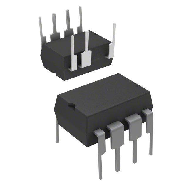
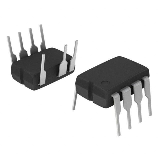
| 产品图片 |
|
| rohs | 符合RoHS无铅 / 符合限制有害物质指令(RoHS)规范要求 |
| 产品系列 | 电源管理 IC,开关控制器 ,Texas Instruments UCC28083D- |
| 数据手册 | |
| 产品型号 | UCC28083D |
| PWM类型 | 电流模式 |
| 上升时间 | 25 ns |
| 下降时间 | 25 ns |
| 产品目录页面 | |
| 产品种类 | 开关控制器 |
| 倍增器 | 无 |
| 其它名称 | 296-13676-5 |
| 分频器 | 无 |
| 包装 | 管件 |
| 升压 | 无 |
| 单位重量 | 72.600 mg |
| 占空比 | 50% |
| 占空比-最大 | 50 % |
| 反向 | 无 |
| 反激式 | 无 |
| 商标 | Texas Instruments |
| 安装风格 | SMD/SMT |
| 封装 | Tube |
| 封装/外壳 | 8-SOIC(0.154",3.90mm 宽) |
| 封装/箱体 | SOIC-8 |
| 工作温度 | -40°C ~ 85°C |
| 工厂包装数量 | 75 |
| 开关频率 | 1000 kHz |
| 拓扑结构 | Half-Bridge, Push-Pull |
| 最大工作温度 | + 85 C |
| 最小工作温度 | - 40 C |
| 标准包装 | 75 |
| 电压-电源 | 9 V ~ 15 V |
| 类型 | Current Mode PWM Controllers |
| 系列 | UCC28083 |
| 输出数 | 2 |
| 输出电流 | 1000 mA |
| 输出端数量 | 2 Output |
| 降压 | 无 |
| 隔离式 | 无 |
| 频率-最大值 | 1MHz |


- 商务部:美国ITC正式对集成电路等产品启动337调查
- 曝三星4nm工艺存在良率问题 高通将骁龙8 Gen1或转产台积电
- 太阳诱电将投资9.5亿元在常州建新厂生产MLCC 预计2023年完工
- 英特尔发布欧洲新工厂建设计划 深化IDM 2.0 战略
- 台积电先进制程称霸业界 有大客户加持明年业绩稳了
- 达到5530亿美元!SIA预计今年全球半导体销售额将创下新高
- 英特尔拟将自动驾驶子公司Mobileye上市 估值或超500亿美元
- 三星加码芯片和SET,合并消费电子和移动部门,撤换高东真等 CEO
- 三星电子宣布重大人事变动 还合并消费电子和移动部门
- 海关总署:前11个月进口集成电路产品价值2.52万亿元 增长14.8%

PDF Datasheet 数据手册内容提取
(cid:1)(cid:2)(cid:2)(cid:3)(cid:4)(cid:5)(cid:4)(cid:6)(cid:7) (cid:1)(cid:2)(cid:2)(cid:3)(cid:4)(cid:5)(cid:4)(cid:8)(cid:7) (cid:1)(cid:2)(cid:2)(cid:3)(cid:4)(cid:5)(cid:4)(cid:9)(cid:7) (cid:1)(cid:2)(cid:2)(cid:3)(cid:4)(cid:5)(cid:4)(cid:10) (cid:1)(cid:2)(cid:2)(cid:6)(cid:4)(cid:5)(cid:4)(cid:6)(cid:7) (cid:1)(cid:2)(cid:2)(cid:6)(cid:4)(cid:5)(cid:4)(cid:8)(cid:7) (cid:1)(cid:2)(cid:2)(cid:6)(cid:4)(cid:5)(cid:4)(cid:9)(cid:7) (cid:1)(cid:2)(cid:2)(cid:6)(cid:4)(cid:5)(cid:4)(cid:10) SLUS488E − SEPTEMBER 2002 − REVISED JULY 2009 (cid:4)(cid:11)(cid:12)(cid:13)(cid:14) (cid:2)(cid:1)(cid:15)(cid:15)(cid:16)(cid:14)(cid:17) (cid:18)(cid:19)(cid:20)(cid:16) (cid:12)(cid:1)(cid:21)(cid:22)(cid:11)(cid:12)(cid:1)(cid:23)(cid:23) (cid:12)(cid:24)(cid:18) (cid:2)(cid:19)(cid:14)(cid:17)(cid:15)(cid:19)(cid:23)(cid:23)(cid:16)(cid:15)(cid:21) (cid:24)(cid:13)(cid:17)(cid:22) (cid:12)(cid:15)(cid:19)(cid:25)(cid:15)(cid:26)(cid:18)(cid:18)(cid:26)(cid:27)(cid:23)(cid:16) (cid:21)(cid:23)(cid:19)(cid:12)(cid:16) (cid:2)(cid:19)(cid:18)(cid:12)(cid:16)(cid:14)(cid:21)(cid:26)(cid:17)(cid:13)(cid:19)(cid:14) FEATURES APPLICATIONS (cid:1) (cid:1) Programmable Slope Compensation High-Efficiency Switch-Mode Power Supplies (cid:1) (cid:1) Internal Soft-Start on the UCC38083/4 Telecom dc-to-dc Converters (cid:1) (cid:1) Cycle-by-Cycle Current Limiting Point-of-Load or Point-of-Use Power Modules (cid:1) Low Start-Up Current of 120 µA and 1.5 mA (cid:1) Low-Cost Push-Pull and Half-Bridge Typical Run Current Applications (cid:1) Single External Component Oscillator DESCRIPTION Programmable from 50 kHz to 1 MHz (cid:1) High-Current Totem-Pole Dual Output Stage The UCC38083/4/5/6 is a family of BiCMOS pulse width Drives Push-Pull Configuration with 1-A Sink modulation (PWM) controllers for dc-to-dc or off-line fixed-frequency current-mode switching power and 0.5-A Source Capability supplies. The dual output stages are configured for the (cid:1) Current Sense Discharge Transistor to push-pull topology. Both outputs switch at half the Improve Dynamic Response oscillator frequency using a toggle flip-flop. The dead (cid:1) time between the two outputs is typically 110 ns, limiting Internally Trimmed Bandgap Reference each output’s duty cycle to less than 50%. (cid:1) Undervoltage Lockout with Hysteresis The new UCC3808x family is based on the UCC3808A architecture. The major differences include the addition BASIC APPLICATION of a programmable slope compensation ramp to the CS signal and the removal of the error amplifier. The current flowing out of the ISET pin through an external resistor is monitored internally to set the magnitude of the slope VIN TRANPSOFWOERRMER VOUTcinotemrpneanl dsaistciohna rfguen ctrtaionns.i sTtohri sfr odmev tihcee CaSls op inin tcolu gdreosu nadn, which is activated at each clock cycle after the pulse is terminated. This discharges any filter capacitance on VDD the CS pin during each cycle and helps minimize filter UCC3808x capacitor values and current sense delay. CTRL OUTA The UCC38083 and the UCC38084 devices have a typical soft-start interval time of 3.5 ms while the RT OUTB UCC38085 and the UCC38086 has less than 100 µs for applications where internal soft-start is not desired. RF ISET CS The UCC38083 and the UCC38085 devices have the RT GND turn-on/off thresholds of 12.5 V / 8.3 V, while the RSET CF RS UthCreCs3h8o0ld8s4 o fa 4n.3d Vt h/ e4 .1U VC. CEa3c8h0 8d6e vihcaes i s tohfefe rteudr nin-o 8n-/poifnf TSSOP (PW), 8-pin SOIC (D) and 8-pin PDIP (P) packages. FEEDBACK UDG−01080 Please be aware that an important notice concerning availability, standard warranty, and use in critical applications of TexasInstruments semiconductor products and disclaimers thereto appears at the end of this data sheet. (cid:12)(cid:15)(cid:19)(cid:20)(cid:1)(cid:2)(cid:17)(cid:13)(cid:19)(cid:14) (cid:20)(cid:26)(cid:17)(cid:26) (cid:28)(cid:29)(cid:30)(cid:31)!"#$(cid:28)(cid:31)(cid:29) (cid:28)% &’!!((cid:29)$ #% (cid:31)(cid:30) )’*+(cid:28)&#$(cid:28)(cid:31)(cid:29) ,#$(- Copyright 2002−2009, Texas Instruments Incorporated (cid:12)!(cid:31),’&$% &(cid:31)(cid:29)(cid:30)(cid:31)!" $(cid:31) %)(&(cid:28)(cid:30)(cid:28)&#$(cid:28)(cid:31)(cid:29)% )(! $.( $(!"% (cid:31)(cid:30) (cid:17)(/#% (cid:13)(cid:29)%$!’"((cid:29)$% %$#(cid:29),#!, 0#!!#(cid:29)$1- (cid:12)!(cid:31),’&$(cid:28)(cid:31)(cid:29) )!(cid:31)&(%%(cid:28)(cid:29)2 ,(cid:31)(% (cid:29)(cid:31)$ (cid:29)(&(%%#!(cid:28)+1 (cid:28)(cid:29)&+’,( $(%$(cid:28)(cid:29)2 (cid:31)(cid:30) #++ )#!#"($(!%- www.ti.com 1
(cid:1)(cid:2)(cid:2)(cid:3)(cid:4)(cid:5)(cid:4)(cid:6)(cid:7) (cid:1)(cid:2)(cid:2)(cid:3)(cid:4)(cid:5)(cid:4)(cid:8)(cid:7) (cid:1)(cid:2)(cid:2)(cid:3)(cid:4)(cid:5)(cid:4)(cid:9)(cid:7) (cid:1)(cid:2)(cid:2)(cid:3)(cid:4)(cid:5)(cid:4)(cid:10) (cid:1)(cid:2)(cid:2)(cid:6)(cid:4)(cid:5)(cid:4)(cid:6)(cid:7) (cid:1)(cid:2)(cid:2)(cid:6)(cid:4)(cid:5)(cid:4)(cid:8)(cid:7) (cid:1)(cid:2)(cid:2)(cid:6)(cid:4)(cid:5)(cid:4)(cid:9)(cid:7) (cid:1)(cid:2)(cid:2)(cid:6)(cid:4)(cid:5)(cid:4)(cid:10) SLUS488E − SEPTEMBER 2002 − REVISED JULY 2009 ORDERING INFORMATION THERMAL RESISTANCE TABLE PACKAGE θjc(°C/W) θja(°C/W) SOIC−8 (D) 42 84 to 160(1) PDIP−8 (P) 50 110(1) TSSOP−8 (PW) 32(2) 232 to 257(2) NOTES: (1) Specified θja (junction to ambient) is for devices mounted to 5-inch2 FR4 PC board with one ounce copper where noted. When resistance range is given, lower values are for 5 inch2 aluminum PC board. Test PWB was 0.062 inch thick and typically used 0.635-mm trace widths for power packages and 1.3-mm trace widths for non-power packages with a 100-mil x 100-mil probe land area at the end of each trace. (2). Modeled data. If value range given for θja, lower value is for 3x3 inch. 1 oz internal copper ground plane, higher value is for 1x1-inch. ground plane. All model data assumes only one trace for each non-fused lead. AVAILABLE OPTIONS IINNTTEERRNNAALL UVLO PACKAGES TTAA SSOOFFTT SSTTAARRTT ON OFF SOIC-8 (D) PDIP-8 (P) TSSOP-8 (PW) 12.5 V 8.3 V UCC28083D UCC28083P UCC28083PW 33..55 mmss 4.3 V 4.1 V UCC28084D UCC28084P UCC28084PW −−4400°°CC ttoo 8855°°CC 12.5 V 8.3 V UCC28085D UCC28085P UCC28085PW 7755 µµss 4.3 V 4.1 V UCC28086D UCC28086P UCC28086PW 12.5 V 8.3 V UCC38083D UCC38083P UCC38083PW 33..55 mmss 4.3 V 4.1 V UCC38084D UCC38084P UCC38084PW 00°°CC ttoo 7700°°CC 12.5 V 8.3 V UCC38085D UCC38085P UCC38085PW 7755 µµss 4.3 V 4.1 V UCC38086D UCC38086P UCC38086PW †The D and PW packages are available taped and reeled. Add R suffix to device type, e.g. UCC28083DR (2500 devices per reel) or UCC38083PWR (2000 devices per reel). D OR P PACKAGE PW PACKAGE (TOP VIEW) (TOP VIEW) CTRL 1 8 VDD OUTA 1 8 OUTB ISET 2 7 OUTA VDD 2 7 GND CTRL 3 6 RT CS 3 6 OUTB ISET 4 5 CS RT 4 5 GND 2 www.ti.com
(cid:1)(cid:2)(cid:2)(cid:3)(cid:4)(cid:5)(cid:4)(cid:6)(cid:7) (cid:1)(cid:2)(cid:2)(cid:3)(cid:4)(cid:5)(cid:4)(cid:8)(cid:7) (cid:1)(cid:2)(cid:2)(cid:3)(cid:4)(cid:5)(cid:4)(cid:9)(cid:7) (cid:1)(cid:2)(cid:2)(cid:3)(cid:4)(cid:5)(cid:4)(cid:10) (cid:1)(cid:2)(cid:2)(cid:6)(cid:4)(cid:5)(cid:4)(cid:6)(cid:7) (cid:1)(cid:2)(cid:2)(cid:6)(cid:4)(cid:5)(cid:4)(cid:8)(cid:7) (cid:1)(cid:2)(cid:2)(cid:6)(cid:4)(cid:5)(cid:4)(cid:9)(cid:7) (cid:1)(cid:2)(cid:2)(cid:6)(cid:4)(cid:5)(cid:4)(cid:10) SLUS488E − SEPTEMBER 2002 − REVISED JULY 2009 absolute maximum ratings over operating free-air temperature (unless otherwise noted)† Supply voltage, V (I < 10 mA) . . . . . . . . . . . . . . . . . . . . . . . . . . . . . . . . . . . . . . . . . . . . . . . . . . . . . . . . . . . . . 15 V DD DD Supply current, I . . . . . . . . . . . . . . . . . . . . . . . . . . . . . . . . . . . . . . . . . . . . . . . . . . . . . . . . . . . . . . . . . . . . . . . . . . 20 mA DD Sink current (peak): OUTA . . . . . . . . . . . . . . . . . . . . . . . . . . . . . . . . . . . . . . . . . . . . . . . . . . . . . . . . . . . . . . . . . 1.0 A OUTB . . . . . . . . . . . . . . . . . . . . . . . . . . . . . . . . . . . . . . . . . . . . . . . . . . . . . . . . . . . . . . . . . 1.0 A Source current (peak): OUTA . . . . . . . . . . . . . . . . . . . . . . . . . . . . . . . . . . . . . . . . . . . . . . . . . . . . . . . . . . . . . . . . −0.5 A OUTB . . . . . . . . . . . . . . . . . . . . . . . . . . . . . . . . . . . . . . . . . . . . . . . . . . . . . . . . . . . . . . . . −0.5 A Analog inputs: CTRL . . . . . . . . . . . . . . . . . . . . . . . . . . . . . . . . . . . . . . . . . . . . . . . . . . . −0.3 V to V +0.3 V DD CS . . . . . . . . . . . . . . . . . . . . . . . . . . . . . . . . . . . . . −0.3 V to V +0.3 V, not to exceed 6 V DD RSET (minimum) . . . . . . . . . . . . . . . . . . . . . . . . . . . . . . . . . . . . . . . . . . . . . . . . . . . . . . >5 kΩ RT (−100 µA < IRT < 100 µA) . . . . . . . . . . . . . . . . . . . . . . . . . . . . . . . . . . . . . −0.3 V to 2.0 V Power dissipation at T = 25°C (P package) . . . . . . . . . . . . . . . . . . . . . . . . . . . . . . . . . . . . . . . . . . . . . . . . . . . . . 1 W A Power dissipation at T = 25°C (D package) . . . . . . . . . . . . . . . . . . . . . . . . . . . . . . . . . . . . . . . . . . . . . . . . . 650 mW A Power dissipation at T = 25°C (PW package) . . . . . . . . . . . . . . . . . . . . . . . . . . . . . . . . . . . . . . . . . . . . . . . 400 mW A Junction operating temperature, T . . . . . . . . . . . . . . . . . . . . . . . . . . . . . . . . . . . . . . . . . . . . . . . . . . . . −55°C to 150°C J Storage temperature, T . . . . . . . . . . . . . . . . . . . . . . . . . . . . . . . . . . . . . . . . . . . . . . . . . . . . . . . . . . . . −65°C to 150°C stg Lead temperature (soldering 10 seconds) . . . . . . . . . . . . . . . . . . . . . . . . . . . . . . . . . . . . . . . . . . . . . . . . . . . . . . 300°C †Stresses beyond those listed under “absolute maximum ratings” may cause permanent damage to the device. These are stress ratings only, and functional operation of the device at these or any other conditions beyond those indicated under “recommended operating conditions” is not implied. Exposure to absolute-maximum-rated conditions for extended periods may affect device reliability. All voltages are with respect to GND. Currents are positive into, and negative out of the specified terminal. electrical characteristics over recommended operating virtual junction temperature range, V = 10 V (See Note 1),1-µF capacitor from VDD to GND, R = 165 kΩ, R = 1 kΩ, C = 220 pF, DD T F F R = 50 kΩ, T = −40°C to 85°C for UCC2808x, T = 0°C to 70°C for UCC3808x, T = T SET A A A J (unless otherwise noted) overall PARAMETER TEST CONDITIONS MIN TYP MAX UNITS Start-up current VDD < UVLO start threshold voltage 120 200 µA Supply current CTRL = 0 V, CS = 0 V, 1.5 2.5 mA See Note 1 undervoltage lockout PARAMETER TEST CONDITIONS MIN TYP MAX UNITS UCC38083/5 See Note 1 11.5 12.5 13.5 SSttaarrtt tthhrreesshhoolldd vvoollttaaggee UCC38084/6 4.1 4.3 4.5 MMiinniimmuumm ooppeerraattiinngg vvoollttaaggee UCC38083/5 7.6 8.3 9.0 VV after start UCC38084/6 3.9 4.1 4.3 UCC38083/5 3.5 4.2 5.1 HHyysstteerreessiiss vvoollttaaggee UCC38084/6 0.1 0.2 0.3 oscillator PARAMETER TEST CONDITIONS MIN TYP MAX UNITS Frequency 2 x f(OUTA) 180 200 220 kHz Voltage amplitude See Note 2 1.4 1.5 1.6 V Oscillator fall time (dead time) 110 220 ns RT pin voltage 1.2 1.5 1.6 V www.ti.com 3
(cid:1)(cid:2)(cid:2)(cid:3)(cid:4)(cid:5)(cid:4)(cid:6)(cid:7) (cid:1)(cid:2)(cid:2)(cid:3)(cid:4)(cid:5)(cid:4)(cid:8)(cid:7) (cid:1)(cid:2)(cid:2)(cid:3)(cid:4)(cid:5)(cid:4)(cid:9)(cid:7) (cid:1)(cid:2)(cid:2)(cid:3)(cid:4)(cid:5)(cid:4)(cid:10) (cid:1)(cid:2)(cid:2)(cid:6)(cid:4)(cid:5)(cid:4)(cid:6)(cid:7) (cid:1)(cid:2)(cid:2)(cid:6)(cid:4)(cid:5)(cid:4)(cid:8)(cid:7) (cid:1)(cid:2)(cid:2)(cid:6)(cid:4)(cid:5)(cid:4)(cid:9)(cid:7) (cid:1)(cid:2)(cid:2)(cid:6)(cid:4)(cid:5)(cid:4)(cid:10) SLUS488E − SEPTEMBER 2002 − REVISED JULY 2009 electrical characteristics over recommended operating virtual junction temperature range, V = 10 V (See Note 1),1-µF capacitor from VDD to GND, R = 165 kΩ, R = 1 kΩ, C = 220 pF, DD T F F R = 50 kΩ, T = −40°C to 85°C for UCC2808x, T = 0°C to 70°C for UCC3808x, T = T SET A A A J (unless otherwise noted) current sense PARAMETER TEST CONDITIONS MIN TYP MAX UNITS Gain See Note 3 1.9 2.2 2.5 V/V Maximum input signal voltage CTRL = 5 V, See Note 4 0.47 0.52 0.57 V CS to output delay time CTRL = 3.5 V, 0 mV ≤ CS ≤ 600 mV 100 200 ns Source current −200 nA CS = 0.5 V, RT = 2.0 V, Sink current 3 7 12 mA See Note 5 Overcurrent threshold voltage 0.70 0.75 0.80 V CS =0 V, 25°C 0.55 0.70 0.90 V CCTTRRLL ttoo CCSS ooffffsseett vvoollttaaggee CS =0 V 0.37 0.70 1.10 V pulse width modulation PARAMETER TEST CONDITIONS MIN TYP MAX UNITS Maximum duty cycle Measured at OUTA or OUTB, See Note 7 48% 49% 50% Minimum duty cycle CTRL = 0 V 0% output PARAMETER TEST CONDITIONS MIN TYP MAX UNITS Low-level output voltage (OUTA or OUTB) IOUT = 100 mA 0.5 1.0 VV High-level output voltage (OUTA or OUTB) IOUT = −50 mA, (VDD − VOUT), See Note 6 0.5 1.0 Rise time CLOAD = 1 nF 25 60 nnss Fall time CLOAD = 1 nF 25 60 soft-start PARAMETER TEST CONDITIONS MIN TYP MAX UNITS OUTA/OUTB soft-start interval time, CTRL = 1.8 V, CS = 0 V, 1.3 3.5 8.5 ms UCC38083/4 Duty cycle from 0 to full, See Note 8 OUTA/OUTB soft-start interval time, CTRL = 1.8 V, CS = 0 V, 30 75 110 µs UCC38085/6 Duty cycle from 0 to full, See Note 8 slope compensation PARAMETER TEST CONDITIONS MIN TYP MAX UNITS IRAMP, peak ISET, peak = 30 µA,Full duty cycle 125 150 175 µA NOTE 1: For UCCx8083/5, set VDD above the start threshold before setting to 10 V. NOTE 2: Measured at ISET pin. (cid:1)V NOTE 3: Gain is defined by A(cid:1) (cid:1)VCTRL, 0 ≤VCS ≤ 0.4 V. CS NOTE 4: Measured at trip point of latch with CS ramped from 0.4 V to 0.6 V. NOTE 5: This internal current sink on the CS pin is designed to discharge and external filter capacitor. It is not intended to be a dc sink path. NOTE 6: Not 100% production tested. Ensured by design and also by the rise time test. NOTE 7: For devices in PW package, parameter tested at wafer probe. NOTE 8: Ensured by design. 4 www.ti.com
(cid:1)(cid:2)(cid:2)(cid:3)(cid:4)(cid:5)(cid:4)(cid:6)(cid:7) (cid:1)(cid:2)(cid:2)(cid:3)(cid:4)(cid:5)(cid:4)(cid:8)(cid:7) (cid:1)(cid:2)(cid:2)(cid:3)(cid:4)(cid:5)(cid:4)(cid:9)(cid:7) (cid:1)(cid:2)(cid:2)(cid:3)(cid:4)(cid:5)(cid:4)(cid:10) (cid:1)(cid:2)(cid:2)(cid:6)(cid:4)(cid:5)(cid:4)(cid:6)(cid:7) (cid:1)(cid:2)(cid:2)(cid:6)(cid:4)(cid:5)(cid:4)(cid:8)(cid:7) (cid:1)(cid:2)(cid:2)(cid:6)(cid:4)(cid:5)(cid:4)(cid:9)(cid:7) (cid:1)(cid:2)(cid:2)(cid:6)(cid:4)(cid:5)(cid:4)(cid:10) SLUS488E − SEPTEMBER 2002 − REVISED JULY 2009 functional block diagram Soft Start and Fault Latch Bias/UVLO CTRL 1 S Q VREF Iss 0.5V Slope Circuit ISLOPE R 8 Vdd−1 VDD S Q + CT R Css ISLOPE= ISET 2 5 x ISET CS Circuitry PWM Comparator/Latch Output Driver 0.75V 7 80 kΩ OUTA S Q Q 60 kΩ T 0.5V R 0.3 V Q CS 3 6 OUTB Oscillator 1.5V S Q 1.5V ICT R RT 4 5 0.2V CT GND UDG−01081 Terminal Functions TERMINAL NNAAMMEE PACKAGE II//OO DDEESSCCRRIIPPTTIIOONN D OR P CS 3 I The current-sense input to the PWM comparator, the cycle-by-cycle peak current comparator, and the overcurrent comparator. The overcurrent comparator is only intended for fault sensing. Exceeding the overcurrent threshold causes a soft-start cycle. An internal MOSFET discharges the current-sense filter capacitor to improve dynamic performance of the power converter. CTRL 1 I Error voltage input to PWM comparator. GND 5 − Reference ground and power ground for all functions. Due to high currents, and high-frequency operation of the IC, a low-impedance circuit board ground plane is highly recommended. ISET 2 I Current selection for slope compensation. OUTA 7 O AAlltteerrnnaattiinngg hhiigghh--ccuurrrreenntt oouuttppuutt ssttaaggeess.. OUTB 6 O RT 4 I Programs the oscillator. VDD 8 I Power input connection. www.ti.com 5
(cid:1)(cid:2)(cid:2)(cid:3)(cid:4)(cid:5)(cid:4)(cid:6)(cid:7) (cid:1)(cid:2)(cid:2)(cid:3)(cid:4)(cid:5)(cid:4)(cid:8)(cid:7) (cid:1)(cid:2)(cid:2)(cid:3)(cid:4)(cid:5)(cid:4)(cid:9)(cid:7) (cid:1)(cid:2)(cid:2)(cid:3)(cid:4)(cid:5)(cid:4)(cid:10) (cid:1)(cid:2)(cid:2)(cid:6)(cid:4)(cid:5)(cid:4)(cid:6)(cid:7) (cid:1)(cid:2)(cid:2)(cid:6)(cid:4)(cid:5)(cid:4)(cid:8)(cid:7) (cid:1)(cid:2)(cid:2)(cid:6)(cid:4)(cid:5)(cid:4)(cid:9)(cid:7) (cid:1)(cid:2)(cid:2)(cid:6)(cid:4)(cid:5)(cid:4)(cid:10) SLUS488E − SEPTEMBER 2002 − REVISED JULY 2009 detailed pin descriptions CTRL: The error voltage is typically generated by a secondary-side error amplifier and transmitted to the primary-side referenced UCC3808x by means of an opto-coupler. CTRL has an internal divider ratio of 0.45 to maintain a usable range with the minimum V of 4.1 V. The UCC38083/UCC38084 family features a built-in DD full-cycle soft start while the UCC38085/6 does not. For the UCC38083/4, soft-start is implemented as a clamp at the input to the PWM comparator. This causes the output pulses to start near 0% duty cycle and increase until the clamp exceeds the CTRL voltage. ISET: Program the slope compensation current ramp by connecting a resistor, RSET, from ISET to ground. The voltage of the ISET pin tracks the 1.5-V internal oscillator ramp, as shown in Figure 1. VCS VDD 10 k(cid:2) IRAMP, peak = 5 x ISET, peak IRAMP UCC38083 IRAMP 1R kF(cid:2) 1 CTRL VDD 8 ISET 2 ISET OUTA 7 1(cid:1)F 3 CS OUTB 6 OUTA 220(cid:1)F 4 RT GND 5 RT 165 k(cid:2) OUTB Figure 1. Full Duty Cycle Output The compensating current source, I , at the CS pin is proportional to the ISET current, according to the SLOPE relation: I (cid:1)5(cid:2)I SLOPE SET (1) The ramping current due to I develops a voltage across the effective filter impedance that is normally SLOPE connected from the current sense resistor to the CS input. In order to program a desired compensating slope with a specific peak compensating ramp voltage at the CS pin, use the RSET value in the following equation: (cid:3) (cid:4) RSET(cid:1)V (cid:2) 5(cid:2)RF OSC(peak) RAMPVOLTAGEHEIGHT (2) Where V (cid:1)1.5V OSC(peak) Notice that the PWM Latch drives an internal MOSFET that will discharge an external filtering capacitor on the CS pin. Thus, I will appear to terminate when the PWM comparator or the cycle-by-cycle current limit SLOPE comparator sets the PWM latch. The actual compensating slope is not affected by premature termination of the switching cycle. 6 www.ti.com
(cid:1)(cid:2)(cid:2)(cid:3)(cid:4)(cid:5)(cid:4)(cid:6)(cid:7) (cid:1)(cid:2)(cid:2)(cid:3)(cid:4)(cid:5)(cid:4)(cid:8)(cid:7) (cid:1)(cid:2)(cid:2)(cid:3)(cid:4)(cid:5)(cid:4)(cid:9)(cid:7) (cid:1)(cid:2)(cid:2)(cid:3)(cid:4)(cid:5)(cid:4)(cid:10) (cid:1)(cid:2)(cid:2)(cid:6)(cid:4)(cid:5)(cid:4)(cid:6)(cid:7) (cid:1)(cid:2)(cid:2)(cid:6)(cid:4)(cid:5)(cid:4)(cid:8)(cid:7) (cid:1)(cid:2)(cid:2)(cid:6)(cid:4)(cid:5)(cid:4)(cid:9)(cid:7) (cid:1)(cid:2)(cid:2)(cid:6)(cid:4)(cid:5)(cid:4)(cid:10) SLUS488E − SEPTEMBER 2002 − REVISED JULY 2009 detailed pin descriptions (continued) OUTA and OUTB: Alternating high-current output stages. Both stages are capable of driving the gate of a power MOSFET. Each stage is capable of 500-mA peak-source current, and 1-A peak-sink current. The output stages switch at half the oscillator frequency, in a push-pull configuration. When the voltage on the internal oscillator capacitor is rising, one of the two outputs is high, but during fall time, both outputs are off. This dead time between the two outputs, along with a slower output rise time than fall time, ensures that the two outputs cannot be on at the same time. This dead time is typically 110 ns. The high-current output drivers consist of MOSFET output devices, which switch from VDD to GND. Each output stage also provides a very low impedance to overshoot and undershoot. This means that in many cases, external Schottky clamp diodes are not required. RT: The oscillator programming pin. The oscillator features an internal timing capacitor. An external resistor, R , sets a current from the RT pin to ground. Due to variations in the internal C , nominal V of 1.5 V can vary T T RT from 1.2 V to 1.6 V Selecting RT as shown programs the oscillator frequency: (cid:3) (cid:4) RT(cid:1) 1 1 (cid:5)2.0(cid:2)10−7 28.7(cid:2)10−12 f OSC (3) where f is in Hz, resistance in Ω. The recommended range of timing resistors is between 25 kΩ and 698 kΩ. OSC For best performance, keep the timing resistor lead from the RT pin to GND (pin 5) as short as possible. 1.5 V S Q 1.5 V IRT ICT R 4 OSCILLATOR CT 0.2 V OUTPUT R T ApproximateFrequency (cid:1)28.7(cid:2)10−12(cid:2)R1 (cid:6)(cid:3)2.0(cid:2)10−7(cid:4) T UDG−01083 Figure 2. Block Diagram for Oscillator VDD: The power input connection for this device. Although quiescent VDD current is very low, total supply current may be higher, depending on OUTA and OUTB current, and the programmed oscillator frequency. Total VDD current is the sum of quiescent VDD current and the average OUT current. Knowing the operating frequency and the MOSFET gate charge (Q ), average OUT current can be calculated from: G I (cid:1)Q (cid:2)f OUT G OSC (4) where f is the oscillator frequency. To prevent noise problems, bypass VDD to GND with a ceramic capacitor as close to the chip as possible along with an electrolytic capacitor. A 1-µF decoupling capacitor is recommended. www.ti.com 7
(cid:1)(cid:2)(cid:2)(cid:3)(cid:4)(cid:5)(cid:4)(cid:6)(cid:7) (cid:1)(cid:2)(cid:2)(cid:3)(cid:4)(cid:5)(cid:4)(cid:8)(cid:7) (cid:1)(cid:2)(cid:2)(cid:3)(cid:4)(cid:5)(cid:4)(cid:9)(cid:7) (cid:1)(cid:2)(cid:2)(cid:3)(cid:4)(cid:5)(cid:4)(cid:10) (cid:1)(cid:2)(cid:2)(cid:6)(cid:4)(cid:5)(cid:4)(cid:6)(cid:7) (cid:1)(cid:2)(cid:2)(cid:6)(cid:4)(cid:5)(cid:4)(cid:8)(cid:7) (cid:1)(cid:2)(cid:2)(cid:6)(cid:4)(cid:5)(cid:4)(cid:9)(cid:7) (cid:1)(cid:2)(cid:2)(cid:6)(cid:4)(cid:5)(cid:4)(cid:10) SLUS488E − SEPTEMBER 2002 − REVISED JULY 2009 APPLICATION INFORMATION The following application circuit shows an isolated 12-V to 2.5 V push-pull converter with scalable output IN OUT power (20 W to 200 W). Note that the pinout shown is for SOIC-8 and PDIP-8 packages. typical application VO = 2.2 V TO 3.3 V ADJUSTABLE VIN = 12 V +/−20%V SR DRIVE 1 µF 8 4.7Ω VDD 7 OUTA RT 4 UCC3808x 4.7Ω 6 6 OUTB RF 1 kΩ CTRL 1 5 1 3 CS 165 GND ISET kΩ 2 4 5 2 RS 3 CF TL431 220 pF RSET UDG−01084 8 www.ti.com
(cid:1)(cid:2)(cid:2)(cid:3)(cid:4)(cid:5)(cid:4)(cid:6)(cid:7) (cid:1)(cid:2)(cid:2)(cid:3)(cid:4)(cid:5)(cid:4)(cid:8)(cid:7) (cid:1)(cid:2)(cid:2)(cid:3)(cid:4)(cid:5)(cid:4)(cid:9)(cid:7) (cid:1)(cid:2)(cid:2)(cid:3)(cid:4)(cid:5)(cid:4)(cid:10) (cid:1)(cid:2)(cid:2)(cid:6)(cid:4)(cid:5)(cid:4)(cid:6)(cid:7) (cid:1)(cid:2)(cid:2)(cid:6)(cid:4)(cid:5)(cid:4)(cid:8)(cid:7) (cid:1)(cid:2)(cid:2)(cid:6)(cid:4)(cid:5)(cid:4)(cid:9)(cid:7) (cid:1)(cid:2)(cid:2)(cid:6)(cid:4)(cid:5)(cid:4)(cid:10) SLUS488E − SEPTEMBER 2002 − REVISED JULY 2009 APPLICATION INFORMATION operational waveforms Figure 3 illustrates how the voltage ramp is effectively added to the voltage across the current sense element V , to implement slope compensation. CS OUTA OUTB VRS ADDED RAMP VOLTAGE VCS, Pin 3 UDG−01085 Figure 3. Typical Slope Compensation Waveforms at 80% Duty Cycle In Figure 3, OUTA and OUTB are shown at a duty cycle of 80%, with the associated voltage VRS across the current sense resistor of the primary push-pull power MOSFETs. The current flowing out of CS generates the ramp voltage across the filter resistor R that is positioned between the power current sense resistor and the F CS pin. This voltage is effectively added to VRS to provide slope compensation at VCS, pin 3. A capacitor C F is also recommended to filter the waveform at CS. www.ti.com 9
(cid:1)(cid:2)(cid:2)(cid:3)(cid:4)(cid:5)(cid:4)(cid:6)(cid:7) (cid:1)(cid:2)(cid:2)(cid:3)(cid:4)(cid:5)(cid:4)(cid:8)(cid:7) (cid:1)(cid:2)(cid:2)(cid:3)(cid:4)(cid:5)(cid:4)(cid:9)(cid:7) (cid:1)(cid:2)(cid:2)(cid:3)(cid:4)(cid:5)(cid:4)(cid:10) (cid:1)(cid:2)(cid:2)(cid:6)(cid:4)(cid:5)(cid:4)(cid:6)(cid:7) (cid:1)(cid:2)(cid:2)(cid:6)(cid:4)(cid:5)(cid:4)(cid:8)(cid:7) (cid:1)(cid:2)(cid:2)(cid:6)(cid:4)(cid:5)(cid:4)(cid:9)(cid:7) (cid:1)(cid:2)(cid:2)(cid:6)(cid:4)(cid:5)(cid:4)(cid:10) SLUS488E − SEPTEMBER 2002 − REVISED JULY 2009 layout considerations To prevent noise problems, bypass VDD to GND with a ceramic capacitor as close to the chip as possible along with an electrolytic capacitor. A 1-µF decoupling capacitor is recommended. Use a local ground plane near the small signal pins (CTRL, ISET, CS and RT) of the IC for shielding. Connect the local ground plane to the GND pin with a single trace. Do not extend the local ground plane under the power pins (VDD, OUTA, OUTB and GND). Instead, use signal return traces to the GND pin for ground returns on the side of the integrated circuit with the power pins. For best performance, keep the timing resistor lead from RT pin (pin 4) to GND (pin 5) as short as possible. special layout considerations for the TSSOP package Due to the different pinout and smaller lead pitch of the TSSOP package, special attention must be paid to minimize noise problems. The pinout is different because the device had to be rotated 90° to fit into the smaller TSSOP package. For example, the two output pins are now on opposite sides of the package. The traces should not run under the package together as they will couple switching noise into analog pins. Another common problem is when RT and OUTB (pins 6 and 8) are routed together for some distance even though they are not immediate side by side pins. Because of this, when OUTB rises, a voltage spike of upto 400 mV can couple into the RT. This spike causes the internal charge current into CT to be turned off momentarily resulting in lower duty cycle. It is also important that note that the RT pin voltage cannot be stabilized with a capacitor. The RT pin is just a dc voltage to program the internal CT. Instead, keep the OUTB and RT runs short and far from each other and follow the printed wiring board layout suggestions above to fix the problem. reference design A reference design is discussed in 50-W Push-Pull Converter Reference Design Using the UCC38083, TI Literature Number SLUU135. This design controls a push-pull synchronous rectified topology with input range of 18 V to 35 V (24 nominal) and 3.3-V output at 15 A. The schematic is shown in Figure 5 and the board layout for the reference design is shown in Figure 4. Refer to the document for further details. Figure 4. Reference Design Layout 10 www.ti.com
(cid:1)(cid:2)(cid:2)(cid:3)(cid:4)(cid:5)(cid:4)(cid:6)(cid:7) (cid:1)(cid:2)(cid:2)(cid:3)(cid:4)(cid:5)(cid:4)(cid:8)(cid:7) (cid:1)(cid:2)(cid:2)(cid:3)(cid:4)(cid:5)(cid:4)(cid:9)(cid:7) (cid:1)(cid:2)(cid:2)(cid:3)(cid:4)(cid:5)(cid:4)(cid:10) (cid:1)(cid:2)(cid:2)(cid:6)(cid:4)(cid:5)(cid:4)(cid:6)(cid:7) (cid:1)(cid:2)(cid:2)(cid:6)(cid:4)(cid:5)(cid:4)(cid:8)(cid:7) (cid:1)(cid:2)(cid:2)(cid:6)(cid:4)(cid:5)(cid:4)(cid:9)(cid:7) (cid:1)(cid:2)(cid:2)(cid:6)(cid:4)(cid:5)(cid:4)(cid:10) SLUS488E − SEPTEMBER 2002 − REVISED JULY 2009 APPLICATION INFORMATION + + oot. h s er v o e g a olt v ut p ut o nt e v e pr d n a p u art- st at k c a b d e e e f d si y ar d n o c e s e h o t ontrol t5 only. 16REG_INVCC38GNDREG_OUT271IN1OUT452IN2OUT See Note 2 12 accelerate the cd for the UCC3808 De d us 5, anents 2n Ro 8, mp 2o CC 1. 2. + e e otot NN Figure 5. Reference Design Schematic www.ti.com 11
(cid:1)(cid:2)(cid:2)(cid:3)(cid:4)(cid:5)(cid:4)(cid:6)(cid:7) (cid:1)(cid:2)(cid:2)(cid:3)(cid:4)(cid:5)(cid:4)(cid:8)(cid:7) (cid:1)(cid:2)(cid:2)(cid:3)(cid:4)(cid:5)(cid:4)(cid:9)(cid:7) (cid:1)(cid:2)(cid:2)(cid:3)(cid:4)(cid:5)(cid:4)(cid:10) (cid:1)(cid:2)(cid:2)(cid:6)(cid:4)(cid:5)(cid:4)(cid:6)(cid:7) (cid:1)(cid:2)(cid:2)(cid:6)(cid:4)(cid:5)(cid:4)(cid:8)(cid:7) (cid:1)(cid:2)(cid:2)(cid:6)(cid:4)(cid:5)(cid:4)(cid:9)(cid:7) (cid:1)(cid:2)(cid:2)(cid:6)(cid:4)(cid:5)(cid:4)(cid:10) SLUS488E − SEPTEMBER 2002 − REVISED JULY 2009 TYPICAL CHARACTERISTICS OSCILLATOR FREQUENCY OSCILLATOR FREQUENCY vs vs TIMING RESISTANCE TEMPERATURE 220 1200 RT = 165 kΩ″ RF= 1 kΩ T = 85°C 215 CF = 220 kΩ 1000 VDD = 15 V RSET = 50 kΩ 210 800 T = 25°C Hz 205 z VDD = 10 V − k − kH 600 ncy 200 uency Freque 195 q 400 e r F 190 200 T = 40°C 185 VDD = 6 V 180 0 −50 −25 0 25 50 75 100 125 10 100 1000 RT − Timing Resistance − kΩ Temperature − °C Figure 6 Figure 7 IDD IDD vs vs OSCILLATOR FREQUENCY, (NO LOAD) OSCILLATOR FREQUENCY, 1 nF LOAD 12 25 VDD = 14 V 10 VDD = 14 V 20 8 VDD = 10 V 15 mA 6 VDD = 10 V mA − − D D 10 VDD = 6 V D D I I 4 VDD = 6 V 5 2 0 0 10 100 1000 10 100 1000 Frequency − kHz Frequency − kHz Figure 8 Figure 9 12 www.ti.com
(cid:1)(cid:2)(cid:2)(cid:3)(cid:4)(cid:5)(cid:4)(cid:6)(cid:7) (cid:1)(cid:2)(cid:2)(cid:3)(cid:4)(cid:5)(cid:4)(cid:8)(cid:7) (cid:1)(cid:2)(cid:2)(cid:3)(cid:4)(cid:5)(cid:4)(cid:9)(cid:7) (cid:1)(cid:2)(cid:2)(cid:3)(cid:4)(cid:5)(cid:4)(cid:10) (cid:1)(cid:2)(cid:2)(cid:6)(cid:4)(cid:5)(cid:4)(cid:6)(cid:7) (cid:1)(cid:2)(cid:2)(cid:6)(cid:4)(cid:5)(cid:4)(cid:8)(cid:7) (cid:1)(cid:2)(cid:2)(cid:6)(cid:4)(cid:5)(cid:4)(cid:9)(cid:7) (cid:1)(cid:2)(cid:2)(cid:6)(cid:4)(cid:5)(cid:4)(cid:10) SLUS488E − SEPTEMBER 2002 − REVISED JULY 2009 TYPICAL CHARACTERISTICS DEAD TIME DEAD TIME vs vs TIMING RESISTANCE OVER VDD TEMPERATURE 200 160 RT = 165 kΩ″ 180 RF= 1 kΩ 160 T = 25°C VT D=D 8 5=° C6 V* 140 CRFS E=T 2 =2 05 0k ΩkΩ 120 140 VDD = 6 V* VDD = 10 V s s n 100 e − n 120 me − d Tim 100 VDD = 14 V ad Ti 80 a 80 e De D 60 60 VDD = 14 V T = −40°C 40 40 20 20 * UCCx8084/6, only 0 0 10 100 1000 −50 −25 0 25 50 75 100 125 RT − Timing Resistance − kΩ Temperature −°C Figure 10 Figure 11 CONTROL TO CS OFFSET RAMP HEIGHT vs vs TEMPERATURE VDD 2.0 0.6 TA = 25°C (OC Clamped) 1.8 RSET = 10 kΩ 0.5 1.6 V − ge 1.4 VCS = 0.40 V RSET = 18 kΩ a 0.4 rol Volt 1.2 − Vs) ont 1.0 K(c 0.3 C P − 0.8 V L TR 0.2 C 0.6 V RSET = 50 kΩ 0.4 VCS = 0 V 0.1 0.2 RSET = 100 kΩ 0.0 0 −50 −25 0 25 50 75 100 125 0 5 10 15 Temperature − °C VDD − Volts Figure 12 Figure 13 www.ti.com 13
(cid:1)(cid:2)(cid:2)(cid:3)(cid:4)(cid:5)(cid:4)(cid:6)(cid:7) (cid:1)(cid:2)(cid:2)(cid:3)(cid:4)(cid:5)(cid:4)(cid:8)(cid:7) (cid:1)(cid:2)(cid:2)(cid:3)(cid:4)(cid:5)(cid:4)(cid:9)(cid:7) (cid:1)(cid:2)(cid:2)(cid:3)(cid:4)(cid:5)(cid:4)(cid:10) (cid:1)(cid:2)(cid:2)(cid:6)(cid:4)(cid:5)(cid:4)(cid:6)(cid:7) (cid:1)(cid:2)(cid:2)(cid:6)(cid:4)(cid:5)(cid:4)(cid:8)(cid:7) (cid:1)(cid:2)(cid:2)(cid:6)(cid:4)(cid:5)(cid:4)(cid:9)(cid:7) (cid:1)(cid:2)(cid:2)(cid:6)(cid:4)(cid:5)(cid:4)(cid:10) SLUS488E − SEPTEMBER 2002 − REVISED JULY 2009 TYPICAL CHARACTERISTICS RAMP HEIGHT RAMP HEIGHT vs vs RT TEMPERATURE 0.7 0.6 TA = 25°C RSET = 10 kΩ (OC Clamped) 0.6 0.5 (OC Clamped) 0.5 RSET = 10 kΩ RSET = 18 kΩ 0.4 V V − − K(cs) 0.4 RSET = 18 kΩ PK(cs) 0.3 VP 0.3 V 0.2 RSET = 50 kΩ 0.2 RSET = 50 kΩ 0.1 0.1 RSET = 100 kΩ RSET = 100 kΩ 0 0.0 10 100 1000 −50 −25 0 25 50 75 100 125 RT − kΩ Temperature − ° C Figure 14 Figure 15 SOFT START SOFT START vs vs TEMPERATURE TEMPERATURE 6 100 UCCx8083 AND UCCx8084 UCCx8085 AND UCCx8086 95 5 90 ms 4 µ− s 85 al − nal 80 oft Start Intern 23 Soft Start Inter 767055 S 60 1 55 0 50 −50 −25 0 25 50 75 100 125 −50 −25 0 25 50 75 100 125 Temperature − °C Temperature − °C Figure 16 Figure 17 14 www.ti.com
(cid:1)(cid:2)(cid:2)(cid:3)(cid:4)(cid:5)(cid:4)(cid:6)(cid:7) (cid:1)(cid:2)(cid:2)(cid:3)(cid:4)(cid:5)(cid:4)(cid:8)(cid:7) (cid:1)(cid:2)(cid:2)(cid:3)(cid:4)(cid:5)(cid:4)(cid:9)(cid:7) (cid:1)(cid:2)(cid:2)(cid:3)(cid:4)(cid:5)(cid:4)(cid:10) (cid:1)(cid:2)(cid:2)(cid:6)(cid:4)(cid:5)(cid:4)(cid:6)(cid:7) (cid:1)(cid:2)(cid:2)(cid:6)(cid:4)(cid:5)(cid:4)(cid:8)(cid:7) (cid:1)(cid:2)(cid:2)(cid:6)(cid:4)(cid:5)(cid:4)(cid:9)(cid:7) (cid:1)(cid:2)(cid:2)(cid:6)(cid:4)(cid:5)(cid:4)(cid:10) SLUS488E − SEPTEMBER 2002 − REVISED JULY 2009 TYPICAL CHARACTERISTICS CS TO OUTX DELAY TIME vs TEMPERATURE 150 140 130 ns 120 − y a 110 el D p 100 o r P S 90 C 80 70 60 50 −50 −25 0 25 50 75 100 125 Temperature − °C Figure 18 RELATED PRODUCTS UCC3808, 8-Pin Low Power Current Mode Push-Pull PWM, (SLUS168) UCC3808A, 8-Pin Low-Power Current-Mode Push-Pull PWM, (SLUS456) UCC3806, Low Power, Dual Output, Current Mode PWM Controller, (SLUS272) Table 1. 8-Pin Push-Pull PWM Controller Family Feature Comparison Programmable CS Error Internal Part Number UVLO On UVLO Off Slope Discharge FET Amplifier Softstart Compensation UCC38083 12.5 V 8.3 V Yes No Yes Yes UCC38084 4.3 V 4.1 V Yes No Yes Yes UCC38085 12.5 V 8.3 V Yes No Yes No UCC38086 4.3 V 4.1 V Yes No Yes No UCC3808A−1 12.5 V 8.3 V Yes Yes No Yes UCC3808A−2 4.3 V 4.1 V Yes Yes No Yes UCC3808−1 12.5 V 8.3 V No Yes No Yes UCC3808−2 4.3 V 4.1 V No Yes No Yes www.ti.com 15
PACKAGE OPTION ADDENDUM www.ti.com 24-Aug-2018 PACKAGING INFORMATION Orderable Device Status Package Type Package Pins Package Eco Plan Lead/Ball Finish MSL Peak Temp Op Temp (°C) Device Marking Samples (1) Drawing Qty (2) (6) (3) (4/5) UCC28083D ACTIVE SOIC D 8 75 Green (RoHS CU NIPDAU Level-1-260C-UNLIM -40 to 85 28083 & no Sb/Br) UCC28083DG4 ACTIVE SOIC D 8 75 Green (RoHS CU NIPDAU Level-1-260C-UNLIM -40 to 85 28083 & no Sb/Br) UCC28083DR ACTIVE SOIC D 8 2500 Green (RoHS CU NIPDAU Level-1-260C-UNLIM -40 to 85 28083 & no Sb/Br) UCC28083DRG4 ACTIVE SOIC D 8 2500 Green (RoHS CU NIPDAU Level-1-260C-UNLIM -40 to 85 28083 & no Sb/Br) UCC28083P ACTIVE PDIP P 8 50 Green (RoHS CU NIPDAU N / A for Pkg Type -40 to 85 UCC28083P & no Sb/Br) UCC28083PW ACTIVE TSSOP PW 8 150 Green (RoHS CU NIPDAU Level-2-260C-1 YEAR -40 to 85 28083 & no Sb/Br) UCC28084D ACTIVE SOIC D 8 75 Green (RoHS CU NIPDAU Level-1-260C-UNLIM -40 to 85 28084 & no Sb/Br) UCC28084DR ACTIVE SOIC D 8 2500 Green (RoHS CU NIPDAU Level-1-260C-UNLIM -40 to 85 28084 & no Sb/Br) UCC28084DRG4 ACTIVE SOIC D 8 2500 Green (RoHS CU NIPDAU Level-1-260C-UNLIM -40 to 85 28084 & no Sb/Br) UCC28084P ACTIVE PDIP P 8 50 Green (RoHS CU NIPDAU N / A for Pkg Type -40 to 85 UCC28084P & no Sb/Br) UCC28084PW ACTIVE TSSOP PW 8 150 Green (RoHS CU NIPDAU Level-2-260C-1 YEAR -40 to 85 28084 & no Sb/Br) UCC28084PWG4 ACTIVE TSSOP PW 8 150 Green (RoHS CU NIPDAU Level-2-260C-1 YEAR -40 to 85 28084 & no Sb/Br) UCC28084PWR ACTIVE TSSOP PW 8 2000 Green (RoHS CU NIPDAU Level-2-260C-1 YEAR -40 to 85 28084 & no Sb/Br) UCC28084PWRG4 ACTIVE TSSOP PW 8 2000 Green (RoHS CU NIPDAU Level-2-260C-1 YEAR -40 to 85 28084 & no Sb/Br) UCC28085D ACTIVE SOIC D 8 75 Green (RoHS CU NIPDAU Level-1-260C-UNLIM -40 to 85 28085 & no Sb/Br) UCC28085DR ACTIVE SOIC D 8 2500 Green (RoHS CU NIPDAU Level-1-260C-UNLIM -40 to 85 28085 & no Sb/Br) UCC28085P ACTIVE PDIP P 8 50 Green (RoHS CU NIPDAU N / A for Pkg Type -40 to 85 UCC28085P & no Sb/Br) Addendum-Page 1
PACKAGE OPTION ADDENDUM www.ti.com 24-Aug-2018 Orderable Device Status Package Type Package Pins Package Eco Plan Lead/Ball Finish MSL Peak Temp Op Temp (°C) Device Marking Samples (1) Drawing Qty (2) (6) (3) (4/5) UCC28085PW ACTIVE TSSOP PW 8 150 Green (RoHS CU NIPDAU Level-2-260C-1 YEAR -40 to 85 28085 & no Sb/Br) UCC28086D ACTIVE SOIC D 8 75 Green (RoHS CU NIPDAU Level-1-260C-UNLIM -40 to 85 28086 & no Sb/Br) UCC28086DR ACTIVE SOIC D 8 2500 Green (RoHS CU NIPDAU Level-1-260C-UNLIM -40 to 85 28086 & no Sb/Br) UCC28086P ACTIVE PDIP P 8 50 Green (RoHS CU NIPDAU N / A for Pkg Type -40 to 85 UCC28086P & no Sb/Br) UCC28086PW ACTIVE TSSOP PW 8 150 Green (RoHS CU NIPDAU Level-2-260C-1 YEAR -40 to 85 28086 & no Sb/Br) UCC28086PWR ACTIVE TSSOP PW 8 2000 Green (RoHS CU NIPDAU Level-2-260C-1 YEAR -40 to 85 28086 & no Sb/Br) UCC38083D ACTIVE SOIC D 8 75 Green (RoHS CU NIPDAU Level-1-260C-UNLIM 0 to 70 38083 & no Sb/Br) UCC38083DR ACTIVE SOIC D 8 2500 Green (RoHS CU NIPDAU Level-1-260C-UNLIM 0 to 70 38083 & no Sb/Br) UCC38083P ACTIVE PDIP P 8 50 Green (RoHS CU NIPDAU N / A for Pkg Type 0 to 70 UCC38083P & no Sb/Br) UCC38084D ACTIVE SOIC D 8 75 Green (RoHS CU NIPDAU Level-1-260C-UNLIM 0 to 70 38084 & no Sb/Br) UCC38084DR ACTIVE SOIC D 8 2500 Green (RoHS CU NIPDAU Level-1-260C-UNLIM 0 to 70 38084 & no Sb/Br) UCC38084DRG4 ACTIVE SOIC D 8 2500 Green (RoHS CU NIPDAU Level-1-260C-UNLIM 0 to 70 38084 & no Sb/Br) UCC38084P ACTIVE PDIP P 8 50 Green (RoHS CU NIPDAU N / A for Pkg Type 0 to 70 UCC38084P & no Sb/Br) UCC38084PW ACTIVE TSSOP PW 8 150 Green (RoHS CU NIPDAU Level-2-260C-1 YEAR 0 to 70 38084 & no Sb/Br) UCC38084PWR ACTIVE TSSOP PW 8 2000 Green (RoHS CU NIPDAU Level-2-260C-1 YEAR 0 to 70 38084 & no Sb/Br) UCC38085D ACTIVE SOIC D 8 75 Green (RoHS CU NIPDAU Level-1-260C-UNLIM 0 to 70 38085 & no Sb/Br) UCC38085P ACTIVE PDIP P 8 50 Green (RoHS CU NIPDAU N / A for Pkg Type 0 to 70 UCC38085P & no Sb/Br) UCC38086D ACTIVE SOIC D 8 75 Green (RoHS CU NIPDAU Level-1-260C-UNLIM 0 to 70 38086 & no Sb/Br) Addendum-Page 2
PACKAGE OPTION ADDENDUM www.ti.com 24-Aug-2018 Orderable Device Status Package Type Package Pins Package Eco Plan Lead/Ball Finish MSL Peak Temp Op Temp (°C) Device Marking Samples (1) Drawing Qty (2) (6) (3) (4/5) UCC38086DR ACTIVE SOIC D 8 2500 Green (RoHS CU NIPDAU Level-1-260C-UNLIM 0 to 70 38086 & no Sb/Br) UCC38086P ACTIVE PDIP P 8 50 Green (RoHS CU NIPDAU N / A for Pkg Type 0 to 70 UCC38086P & no Sb/Br) (1) The marketing status values are defined as follows: ACTIVE: Product device recommended for new designs. LIFEBUY: TI has announced that the device will be discontinued, and a lifetime-buy period is in effect. NRND: Not recommended for new designs. Device is in production to support existing customers, but TI does not recommend using this part in a new design. PREVIEW: Device has been announced but is not in production. Samples may or may not be available. OBSOLETE: TI has discontinued the production of the device. (2) RoHS: TI defines "RoHS" to mean semiconductor products that are compliant with the current EU RoHS requirements for all 10 RoHS substances, including the requirement that RoHS substance do not exceed 0.1% by weight in homogeneous materials. Where designed to be soldered at high temperatures, "RoHS" products are suitable for use in specified lead-free processes. TI may reference these types of products as "Pb-Free". RoHS Exempt: TI defines "RoHS Exempt" to mean products that contain lead but are compliant with EU RoHS pursuant to a specific EU RoHS exemption. Green: TI defines "Green" to mean the content of Chlorine (Cl) and Bromine (Br) based flame retardants meet JS709B low halogen requirements of <=1000ppm threshold. Antimony trioxide based flame retardants must also meet the <=1000ppm threshold requirement. (3) MSL, Peak Temp. - The Moisture Sensitivity Level rating according to the JEDEC industry standard classifications, and peak solder temperature. (4) There may be additional marking, which relates to the logo, the lot trace code information, or the environmental category on the device. (5) Multiple Device Markings will be inside parentheses. Only one Device Marking contained in parentheses and separated by a "~" will appear on a device. If a line is indented then it is a continuation of the previous line and the two combined represent the entire Device Marking for that device. (6) Lead/Ball Finish - Orderable Devices may have multiple material finish options. Finish options are separated by a vertical ruled line. Lead/Ball Finish values may wrap to two lines if the finish value exceeds the maximum column width. Important Information and Disclaimer:The information provided on this page represents TI's knowledge and belief as of the date that it is provided. TI bases its knowledge and belief on information provided by third parties, and makes no representation or warranty as to the accuracy of such information. Efforts are underway to better integrate information from third parties. TI has taken and continues to take reasonable steps to provide representative and accurate information but may not have conducted destructive testing or chemical analysis on incoming materials and chemicals. TI and TI suppliers consider certain information to be proprietary, and thus CAS numbers and other limited information may not be available for release. In no event shall TI's liability arising out of such information exceed the total purchase price of the TI part(s) at issue in this document sold by TI to Customer on an annual basis. Addendum-Page 3
PACKAGE MATERIALS INFORMATION www.ti.com 3-Aug-2017 TAPE AND REEL INFORMATION *Alldimensionsarenominal Device Package Package Pins SPQ Reel Reel A0 B0 K0 P1 W Pin1 Type Drawing Diameter Width (mm) (mm) (mm) (mm) (mm) Quadrant (mm) W1(mm) UCC28083DR SOIC D 8 2500 330.0 12.4 6.4 5.2 2.1 8.0 12.0 Q1 UCC28084DR SOIC D 8 2500 330.0 12.4 6.4 5.2 2.1 8.0 12.0 Q1 UCC28084PWR TSSOP PW 8 2000 330.0 12.4 7.0 3.6 1.6 8.0 12.0 Q1 UCC28085DR SOIC D 8 2500 330.0 12.4 6.4 5.2 2.1 8.0 12.0 Q1 UCC28086DR SOIC D 8 2500 330.0 12.4 6.4 5.2 2.1 8.0 12.0 Q1 UCC28086PWR TSSOP PW 8 2000 330.0 12.4 7.0 3.6 1.6 8.0 12.0 Q1 UCC38083DR SOIC D 8 2500 330.0 12.4 6.4 5.2 2.1 8.0 12.0 Q1 UCC38084DR SOIC D 8 2500 330.0 12.4 6.4 5.2 2.1 8.0 12.0 Q1 UCC38084PWR TSSOP PW 8 2000 330.0 12.4 7.0 3.6 1.6 8.0 12.0 Q1 UCC38086DR SOIC D 8 2500 330.0 12.4 6.4 5.2 2.1 8.0 12.0 Q1 PackMaterials-Page1
PACKAGE MATERIALS INFORMATION www.ti.com 3-Aug-2017 *Alldimensionsarenominal Device PackageType PackageDrawing Pins SPQ Length(mm) Width(mm) Height(mm) UCC28083DR SOIC D 8 2500 340.5 338.1 20.6 UCC28084DR SOIC D 8 2500 340.5 338.1 20.6 UCC28084PWR TSSOP PW 8 2000 367.0 367.0 35.0 UCC28085DR SOIC D 8 2500 340.5 338.1 20.6 UCC28086DR SOIC D 8 2500 340.5 338.1 20.6 UCC28086PWR TSSOP PW 8 2000 367.0 367.0 35.0 UCC38083DR SOIC D 8 2500 340.5 338.1 20.6 UCC38084DR SOIC D 8 2500 340.5 338.1 20.6 UCC38084PWR TSSOP PW 8 2000 367.0 367.0 35.0 UCC38086DR SOIC D 8 2500 340.5 338.1 20.6 PackMaterials-Page2
PACKAGE OUTLINE D0008A SOIC - 1.75 mm max height SCALE 2.800 SMALL OUTLINE INTEGRATED CIRCUIT C SEATING PLANE .228-.244 TYP [5.80-6.19] .004 [0.1] C A PIN 1 ID AREA 6X .050 [1.27] 8 1 2X .189-.197 [4.81-5.00] .150 NOTE 3 [3.81] 4X (0 -15 ) 4 5 8X .012-.020 B .150-.157 [0.31-0.51] .069 MAX [3.81-3.98] .010 [0.25] C A B [1.75] NOTE 4 .005-.010 TYP [0.13-0.25] 4X (0 -15 ) SEE DETAIL A .010 [0.25] .004-.010 0 - 8 [0.11-0.25] .016-.050 [0.41-1.27] DETAIL A (.041) TYPICAL [1.04] 4214825/C 02/2019 NOTES: 1. Linear dimensions are in inches [millimeters]. Dimensions in parenthesis are for reference only. Controlling dimensions are in inches. Dimensioning and tolerancing per ASME Y14.5M. 2. This drawing is subject to change without notice. 3. This dimension does not include mold flash, protrusions, or gate burrs. Mold flash, protrusions, or gate burrs shall not exceed .006 [0.15] per side. 4. This dimension does not include interlead flash. 5. Reference JEDEC registration MS-012, variation AA. www.ti.com
EXAMPLE BOARD LAYOUT D0008A SOIC - 1.75 mm max height SMALL OUTLINE INTEGRATED CIRCUIT 8X (.061 ) [1.55] SYMM SEE DETAILS 1 8 8X (.024) [0.6] SYMM (R.002 ) TYP [0.05] 5 4 6X (.050 ) [1.27] (.213) [5.4] LAND PATTERN EXAMPLE EXPOSED METAL SHOWN SCALE:8X SOLDER MASK SOLDER MASK METAL OPENING OPENING METAL UNDER SOLDER MASK EXPOSED METAL EXPOSED METAL .0028 MAX .0028 MIN [0.07] [0.07] ALL AROUND ALL AROUND NON SOLDER MASK SOLDER MASK DEFINED DEFINED SOLDER MASK DETAILS 4214825/C 02/2019 NOTES: (continued) 6. Publication IPC-7351 may have alternate designs. 7. Solder mask tolerances between and around signal pads can vary based on board fabrication site. www.ti.com
EXAMPLE STENCIL DESIGN D0008A SOIC - 1.75 mm max height SMALL OUTLINE INTEGRATED CIRCUIT 8X (.061 ) [1.55] SYMM 1 8 8X (.024) [0.6] SYMM (R.002 ) TYP [0.05] 5 4 6X (.050 ) [1.27] (.213) [5.4] SOLDER PASTE EXAMPLE BASED ON .005 INCH [0.125 MM] THICK STENCIL SCALE:8X 4214825/C 02/2019 NOTES: (continued) 8. Laser cutting apertures with trapezoidal walls and rounded corners may offer better paste release. IPC-7525 may have alternate design recommendations. 9. Board assembly site may have different recommendations for stencil design. www.ti.com
None
PACKAGE OUTLINE PW0008A TSSOP - 1.2 mm max height SCALE 2.800 SMALL OUTLINE PACKAGE C 6.6 TYP SEATING PLANE 6.2 PIN 1 ID A 0.1 C AREA 6X 0.65 8 1 3.1 2X 2.9 NOTE 3 1.95 4 5 0.30 8X 0.19 4.5 1.2 MAX B 0.1 C A B 4.3 NOTE 4 (0.15) TYP SEE DETAIL A 0.25 GAGE PLANE 0.15 0.75 0 - 8 0.05 0.50 DETAIL A TYPICAL 4221848/A 02/2015 NOTES: 1. All linear dimensions are in millimeters. Any dimensions in parenthesis are for reference only. Dimensioning and tolerancing per ASME Y14.5M. 2. This drawing is subject to change without notice. 3. This dimension does not include mold flash, protrusions, or gate burrs. Mold flash, protrusions, or gate burrs shall not exceed 0.15 mm per side. 4. This dimension does not include interlead flash. Interlead flash shall not exceed 0.25 mm per side. 5. Reference JEDEC registration MO-153, variation AA. www.ti.com
EXAMPLE BOARD LAYOUT PW0008A TSSOP - 1.2 mm max height SMALL OUTLINE PACKAGE 8X (1.5) 8X (0.45) SYMM (R0.05) 1 TYP 8 SYMM 6X (0.65) 5 4 (5.8) LAND PATTERN EXAMPLE SCALE:10X SOOPLEDNEINRG MASK METAL MSOELTDAEL RU NMDAESRK SOOPLEDNEINRG MASK 0.05 MAX 0.05 MIN ALL AROUND ALL AROUND NON SOLDER MASK SOLDER MASK DEFINED DEFINED SOLDER MASK DETAILS NOT TO SCALE 4221848/A 02/2015 NOTES: (continued) 6. Publication IPC-7351 may have alternate designs. 7. Solder mask tolerances between and around signal pads can vary based on board fabrication site. www.ti.com
EXAMPLE STENCIL DESIGN PW0008A TSSOP - 1.2 mm max height SMALL OUTLINE PACKAGE 8X (1.5) SYMM (R0.05) TYP 8X (0.45) 1 8 SYMM 6X (0.65) 5 4 (5.8) SOLDER PASTE EXAMPLE BASED ON 0.125 mm THICK STENCIL SCALE:10X 4221848/A 02/2015 NOTES: (continued) 8. Laser cutting apertures with trapezoidal walls and rounded corners may offer better paste release. IPC-7525 may have alternate design recommendations. 9. Board assembly site may have different recommendations for stencil design. www.ti.com
IMPORTANTNOTICEANDDISCLAIMER TIPROVIDESTECHNICALANDRELIABILITYDATA(INCLUDINGDATASHEETS),DESIGNRESOURCES(INCLUDINGREFERENCE DESIGNS),APPLICATIONOROTHERDESIGNADVICE,WEBTOOLS,SAFETYINFORMATION,ANDOTHERRESOURCES“ASIS” ANDWITHALLFAULTS,ANDDISCLAIMSALLWARRANTIES,EXPRESSANDIMPLIED,INCLUDINGWITHOUTLIMITATIONANY IMPLIEDWARRANTIESOFMERCHANTABILITY,FITNESSFORAPARTICULARPURPOSEORNON-INFRINGEMENTOFTHIRD PARTYINTELLECTUALPROPERTYRIGHTS. TheseresourcesareintendedforskilleddevelopersdesigningwithTIproducts.Youaresolelyresponsiblefor(1)selectingtheappropriate TIproductsforyourapplication,(2)designing,validatingandtestingyourapplication,and(3)ensuringyourapplicationmeetsapplicable standards,andanyothersafety,security,orotherrequirements.Theseresourcesaresubjecttochangewithoutnotice.TIgrantsyou permissiontousetheseresourcesonlyfordevelopmentofanapplicationthatusestheTIproductsdescribedintheresource.Other reproductionanddisplayoftheseresourcesisprohibited.NolicenseisgrantedtoanyotherTIintellectualpropertyrightortoanythird partyintellectualpropertyright.TIdisclaimsresponsibilityfor,andyouwillfullyindemnifyTIanditsrepresentativesagainst,anyclaims, damages,costs,losses,andliabilitiesarisingoutofyouruseoftheseresources. TI’sproductsareprovidedsubjecttoTI’sTermsofSale(www.ti.com/legal/termsofsale.html)orotherapplicabletermsavailableeitheron ti.comorprovidedinconjunctionwithsuchTIproducts.TI’sprovisionoftheseresourcesdoesnotexpandorotherwisealterTI’sapplicable warrantiesorwarrantydisclaimersforTIproducts. MailingAddress:TexasInstruments,PostOfficeBox655303,Dallas,Texas75265 Copyright©2019,TexasInstrumentsIncorporated