ICGOO在线商城 > 集成电路(IC) > PMIC - AC-DC 转换器,离线开关 > TEA1751T/N1,518

 Datasheet下载
- 型号: TEA1751T/N1,518
- 制造商: NXP Semiconductors
- 库位|库存: xxxx|xxxx
- 要求:
| 数量阶梯 | 香港交货 | 国内含税 |
| +xxxx | $xxxx | ¥xxxx |
查看当月历史价格
查看今年历史价格
TEA1751T/N1,518产品简介:
ICGOO电子元器件商城为您提供TEA1751T/N1,518由NXP Semiconductors设计生产,在icgoo商城现货销售,并且可以通过原厂、代理商等渠道进行代购。 TEA1751T/N1,518价格参考。NXP SemiconductorsTEA1751T/N1,518封装/规格:PMIC - AC-DC 转换器,离线开关, Converter Offline Flyback Topology 100kHz ~ 150kHz 16-SO。您可以下载TEA1751T/N1,518参考资料、Datasheet数据手册功能说明书,资料中有TEA1751T/N1,518 详细功能的应用电路图电压和使用方法及教程。
型号为TEA1751T/N1,518的芯片由NXP USA Inc.生产,属于PMIC(电源管理集成电路)中的AC-DC转换器和离线开关类别。该器件主要用于高效能、高集成度的电源转换系统中,适用于需要将交流电(AC)转换为直流电(DC)的应用场景。

典型应用场景包括:

1. 电源适配器:用于笔记本电脑、平板电脑等便携设备的电源适配器中,提供高效、稳定的直流输出。
2. 充电器:智能手机、USB-C设备等智能充电装置中,实现快速且安全的充电功能。
3. 工业电源系统:在工业控制设备或自动化系统中作为主电源转换模块,提供可靠的能量转换。
4. LED照明驱动:用于大功率LED照明系统中,实现恒流输出与高效能转换。
5. 家电电源:如洗衣机、空调等家用电器中,作为内部电源系统的AC-DC转换核心。

该芯片集成了控制器与功率开关,支持准谐振工作模式,有助于提高效率并降低电磁干扰(EMI),适合于中高功率密度电源设计。
| 参数 | 数值 |
| 产品目录 | 集成电路 (IC)半导体 |
| 描述 | IC CTRLR GREENCHIP SMPS 16-SOIC交流/直流转换器 GRNCHIP III PRIMARY |
| 产品分类 | |
| 品牌 | NXP Semiconductors |
| 产品手册 | |
| 产品图片 |
|
| rohs | 符合RoHS无铅 / 符合限制有害物质指令(RoHS)规范要求 |
| 产品系列 | 电源管理 IC,交流/直流转换器,NXP Semiconductors TEA1751T/N1,518GreenChip™ III |
| 数据手册 | |
| 产品型号 | TEA1751T/N1,518 |
| 产品种类 | 交流/直流转换器 |
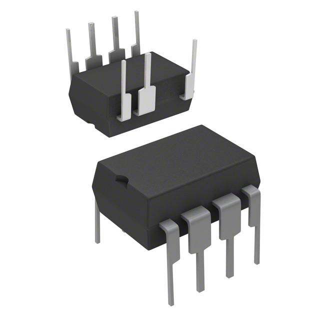
| 供应商器件封装 | 16-SO |
| 其它名称 | 568-4926-6 |
| 功率(W) | 250W |
| 包装 | Digi-Reel® |
| 商标 | NXP Semiconductors |
| 安装风格 | SMD/SMT |
| 封装 | Reel |
| 封装/外壳 | 16-SOIC(0.154",3.90mm 宽) |
| 封装/箱体 | SOIC-16 |
| 工作温度 | -40°C ~ 150°C |
| 工厂包装数量 | 2500 |
| 开关频率 | 125 kHz |
| 标准包装 | 1 |
| 电压-击穿 | 650V |
| 电压-输入 | 70 V ~ 276 VAC |
| 电压-输出 | 10.8V |
| 输出电压 | 11 V |
| 输出电流 | - 1.19 mA |
| 输出隔离 | 隔离 |
| 频率范围 | 100kHz ~ 150kHz |


- 商务部:美国ITC正式对集成电路等产品启动337调查
- 曝三星4nm工艺存在良率问题 高通将骁龙8 Gen1或转产台积电
- 太阳诱电将投资9.5亿元在常州建新厂生产MLCC 预计2023年完工
- 英特尔发布欧洲新工厂建设计划 深化IDM 2.0 战略
- 台积电先进制程称霸业界 有大客户加持明年业绩稳了
- 达到5530亿美元!SIA预计今年全球半导体销售额将创下新高
- 英特尔拟将自动驾驶子公司Mobileye上市 估值或超500亿美元
- 三星加码芯片和SET,合并消费电子和移动部门,撤换高东真等 CEO
- 三星电子宣布重大人事变动 还合并消费电子和移动部门
- 海关总署:前11个月进口集成电路产品价值2.52万亿元 增长14.8%


PDF Datasheet 数据手册内容提取
TEA1751T HV start-up DCM/QR flyback controller with integrated DCM/QR PFC controller Rev. 3 — 10 January 2013 Product data sheet 1. General description The TEA1751T is the third generation of green Switched Mode Power Supply (SMPS) controller ICs. The TEA1751T combines a controller for Power Factor Correction (PFC) and a flyback controller. Its high level of integration allows the design of a cost-effective power supply with a very low number of external components. The special built-in green functions provide high efficiency at all power levels. This efficiency applies to quasi-resonant operation at high-power levels, quasi-resonant operation with valley skipping, as well as reduced frequency operation at lower power levels. At low-power levels, the PFC switches off to maintain high efficiency. During low-power conditions, the flyback controller switches to frequency reduction mode and limits the peak current to 25 % of its maximum value. This mode ensures high efficiency at low-power and good standby power performance while minimizing audible noise from the transformer. The TEA1751T is a Multi-Chip Module, (MCM), containing two chips. The proprietary high-voltage BCD800 process which makes direct start-up possible from the rectified universal mains voltage in an effective and green way. The second low voltage SiliconOnInsulator(SOI) is used for accurate, high speed protection functions and control. The TEA1751T enables the design of highly efficient and reliable supplies with power requirements of up to 250W using the minimum number of external components. Remark: All values provided throughout this data sheet are typical values unless otherwise stated.
TEA1751T NXP Semiconductors HV start-up flyback controller with integrated PFC controller 2. Features and benefits 2.1 Distinctive features Integrated PFC and flyback controller Universal mains supply operation (70V(AC) to276V(AC)) Dual-boost PFC with accurate maximum output voltage (NXP patented) High level of integration, resulting in a very low external component count and a cost-effective design 2.2 Green features On-chip start-up current source 2.3 PFC green features Valley/Zero Voltage Switching (ZVS) for minimum switching losses (NXP patented) Frequency limitation to reduce switching losses PFC is switched off when a low load is detected at the flyback output 2.4 Flyback green features Valley switching for minimum switching losses (NXP patented) Frequency reduction with fixed minimum peak current at low-power operation to maintain high efficiency at low output power levels 2.5 Protection features Safe restart mode for system fault conditions Continuous mode protection with demagnetization detection for both converters (NXP patented) UnderVoltage Protection (UVP) (foldback during overload) Accurate OverVoltage Protection (OVP) for both converters (adjustable for flyback converter) Mains voltage independent OverPower Protection (OPP) Open control loop protection for both converters. The open-loop protection on the flyback converter is safe restart OverTemperature Protection (OTP) Low and adjustable OverCurrent Protection (OCP) trip level for both converters General-purpose input for latched protection to provide system OverTemperature Protection (OTP) for example 3. Applications The device is used in all applications requiring an efficient and cost-effective power supply solutions up to 250W. Notebook adapters in particular can benefit from the high level of integration TEA1751T All information provided in this document is subject to legal disclaimers. © NXP B.V. 2013. All rights reserved. Product data sheet Rev. 3 — 10 January 2013 2 of 31
TEA1751T NXP Semiconductors HV start-up flyback controller with integrated PFC controller 4. Ordering information Table 1. Ordering info rmation Type number Package Name Description Version TEA1751T SO16 plastic small outline package; 16leads; body width 3.9mm SOT109-1 TEA1751T All information provided in this document is subject to legal disclaimers. © NXP B.V. 2013. All rights reserved. Product data sheet Rev. 3 — 10 January 2013 3 of 31
TEA1751T NXP Semiconductors HV start-up flyback controller with integrated PFC controller 5. Block diagram (cid:13)(cid:14)(cid:15))(cid:6)(cid:3)(cid:24)(cid:5)(cid:6)(cid:7) (cid:14)*)(cid:6)(cid:3)(cid:24)(cid:5)(cid:6) /, /= /-/,(cid:7)(cid:24)(cid:7) =-(cid:8)(cid:7)(cid:24)(cid:7) (cid:13)(cid:14)(cid:15)(cid:7) (cid:17)(cid:22)!(cid:20)(cid:17) 6$7#"(cid:21)8(cid:7) (cid:17)(cid:22)!(cid:20)(cid:17) (cid:13)(cid:14)(cid:15)(cid:7)&"(cid:19)(cid:20) (cid:17)(cid:22)!(cid:20)(cid:17) (cid:17)(cid:22)!(cid:20)(cid:17) @(cid:9)(cid:7)(cid:10)’(cid:7)(cid:7) $(cid:18):(cid:7)(cid:24)(cid:22)(cid:23) 6$7#"(cid:21)8(cid:7)&"(cid:19)(cid:20) (cid:20)2(cid:19)(cid:20)(cid:17)(cid:23)"$ (cid:8) (cid:28)’(cid:2)(cid:15)4 (cid:16)(cid:17)(cid:18)(cid:19)(cid:20)(cid:21)(cid:19)(cid:22)(cid:18)(cid:23) /-,(cid:8)(cid:7)(cid:24)(cid:7) (cid:24)(cid:3)(cid:31)(cid:30)(cid:5)(cid:31)(cid:30)(cid:5) . (cid:16)(cid:17)(cid:18)(cid:19)(cid:20)(cid:21)(cid:19)(cid:22)(cid:18)(cid:23) (cid:13)(cid:14)(cid:15)(cid:15)(cid:25)(cid:4)(cid:13) ? #$"3(cid:18)(cid:19)(cid:21)"(cid:18)(cid:26)$(cid:11)(cid:7)(cid:19)(cid:17)(cid:20)(cid:11)(cid:20)(cid:19) (cid:4)’0(cid:3)(cid:4)1(cid:4) (cid:16)(cid:17)(cid:18)(cid:7)(cid:13)(cid:20)(cid:19)(cid:20)(cid:23)(cid:14)(cid:21)"(cid:15)(cid:19)#(cid:22)(cid:18)$(cid:20)(cid:23)(cid:7)(cid:13)(cid:16)(cid:14)(cid:17)(cid:15)(cid:18)(cid:19)(cid:20)(cid:21)(cid:19)(cid:22)(cid:18)(cid:23) (cid:6)(cid:30) 9 9 (cid:6)(cid:30) (cid:20)(cid:23)"#$(cid:20)(cid:7)6$7#"(cid:21)8 6(cid:17)(cid:17)(cid:20)(cid:20); 33(cid:20)(cid:21)(cid:19)(cid:23)(cid:22)(cid:18)(cid:21)(cid:23)7 ,-(cid:8)(cid:7)(cid:24)(cid:7) =-(cid:8)(cid:7)(cid:24)(cid:7) $(cid:18): =(cid:9)(cid:7)(cid:10)’(cid:7)(cid:7) $(cid:18):(cid:7)(cid:16)(cid:18):(cid:20)(cid:17) (cid:16)(cid:18):(cid:20)(cid:17) (cid:13)(cid:14)(cid:15) (cid:14)(cid:28)(*’(cid:15)+ (cid:24)(cid:25)(cid:30)(cid:5)(cid:31)(cid:30)(cid:5) A ,-(cid:8)(cid:9)(cid:7)(cid:24)(cid:7) /-,(cid:8)(cid:7)(cid:24)(cid:7) (cid:25)(cid:30)(cid:15)(cid:3)(cid:28)(cid:28)’(cid:2)(cid:25)(cid:6) (cid:19)(cid:18)(cid:23)(cid:27)%"2(cid:29) (cid:25)(cid:30)(cid:15)(cid:3)(cid:28)(cid:28)’(cid:2)(cid:25)(cid:6) (cid:19)(cid:22)%(cid:20)<(cid:18)3(cid:19) = (cid:14)*(cid:15)(cid:2)(cid:6)(cid:28) =-A(cid:7)(cid:24)(cid:7) /(cid:8)(cid:7)(cid:10)’(cid:7) ,-.(cid:7)(cid:24)(cid:7) (cid:24)(cid:15)(cid:15)(cid:7)&(cid:18)(cid:18) 6(cid:17)(cid:20);3(cid:20)(cid:23)(cid:21)7(cid:7)(cid:17)(cid:20) 3(cid:21)(cid:19)(cid:22)(cid:18)(cid:23) $(cid:18):(cid:7)(cid:16)(cid:18):(cid:20)(cid:17) (cid:30)(cid:4)(cid:13)(cid:30) (cid:11)(cid:19)"(cid:17)(cid:19)(cid:7)6$7#"(cid:21)8 3"$(cid:7)#(cid:18)(cid:18)(cid:11)(cid:19) (cid:20)2(cid:19)(cid:20)(cid:17)(cid:23)"$(cid:7)(cid:16)(cid:17)(cid:18)(cid:19)(cid:20)(cid:21)(cid:19)(cid:22)(cid:18)(cid:23) (cid:15)(cid:25)(cid:31)(cid:2)(cid:6)(cid:25)(cid:28) (cid:11)(cid:19)"(cid:17)(cid:19)(cid:7)(cid:11)(cid:19)(cid:18)(cid:16)(cid:7)(cid:13)(cid:14)(cid:15) (cid:25)(cid:13)(cid:13) (cid:4)(cid:3)(cid:31)(cid:3)(cid:4)1(cid:4) $(cid:18):(cid:7)(cid:24)(cid:22)(cid:23) (cid:24)(cid:18)(cid:7)(cid:25)(cid:24)(cid:13) (cid:13)(cid:14)(cid:15) (cid:2)(cid:5)’/.(cid:8)/(cid:28)(cid:2)(cid:7)(cid:19)(cid:22)%(cid:20)<(cid:18)3(cid:19) (cid:30) (cid:25)(cid:15)(cid:13) (cid:16)(cid:17)(cid:18)(cid:19)(cid:20)(cid:21)(cid:19)(cid:22)(cid:18)(cid:23) (cid:20)2(cid:19)(cid:20)(cid:17)(cid:23)"$(cid:7)(cid:16)(cid:17)(cid:18)(cid:19)(cid:20)(cid:21)(cid:19)(cid:22)(cid:18)(cid:23) (cid:30) (cid:24)(cid:19)(cid:26)(cid:27)(cid:25)(cid:28)(cid:29)(cid:24)(cid:25)(cid:30)(cid:5)(cid:31)(cid:30)(cid:5) (cid:25)(cid:2)(cid:13) (cid:30) (cid:28)’(cid:2)(cid:15)4(cid:5)) (cid:25)(cid:24)(cid:13)(cid:7)6$7#"(cid:21)8 (cid:30)(cid:13)(cid:6)(cid:25)(cid:2)(cid:5)(cid:15)(cid:2)(cid:3)(cid:25)(cid:31) 6$7#"(cid:21)8(cid:7) (cid:17)(cid:22)!(cid:20)(cid:17) *(cid:28)’(cid:31)+ $"(cid:19)(cid:21)(cid:26)(cid:7)(cid:17)(cid:20)(cid:11)(cid:20)(cid:19) (cid:6) /(cid:9) (cid:14)*(cid:30)(cid:5)(cid:31)(cid:30)(cid:5) (cid:25)(cid:15)(cid:13) (cid:2)(cid:5)’/.(cid:8)/(cid:2)(cid:7)(cid:19)(cid:22)%(cid:20)<(cid:18)3(cid:19) (cid:30) (cid:30)’(cid:14)(cid:5) (cid:16)(cid:17)(cid:18)(cid:19)(cid:20)(cid:21)(cid:19)(cid:22)(cid:18)(cid:23) *(cid:28)’(cid:31)+ (cid:13)(cid:14)(cid:15)(cid:7) (cid:17)(cid:22)!(cid:20)(cid:17) (cid:19)(cid:18)(cid:23)(cid:7)%"2 (cid:30) (cid:6)(cid:5)(cid:30)(cid:2)’(cid:6)(cid:2) (cid:20)(cid:23)"#$(cid:20)(cid:7)6$7#"(cid:21)8 ?(cid:9)(cid:7)(cid:10)’(cid:7) (cid:13)(cid:14)(cid:15)(cid:30)(cid:5)(cid:31)(cid:30)(cid:5) // (cid:8)(cid:9)(cid:9)(cid:7)%(cid:24) (cid:20)(cid:23)"#$(cid:20)(cid:7)(cid:13)(cid:14)(cid:15) (cid:24)1(cid:24)(cid:28)(cid:25) (cid:6)(cid:13)(cid:6)(cid:25)(cid:2)(cid:5)(cid:15)(cid:2)(cid:3)(cid:25)(cid:31) (cid:24)(cid:19)(cid:26)(cid:27)(cid:18)$(cid:29)(cid:24)(cid:25)(cid:30)(cid:5)(cid:31)(cid:30)(cid:5) (cid:7)(cid:11)(cid:19)"(cid:17)(cid:19)(cid:7)6$7#"(cid:21)8 (cid:30)(cid:30)(cid:2)(cid:25)’(cid:14)(cid:6)(cid:2)(cid:2) ?(cid:9)(cid:7)(cid:10)’(cid:7)(cid:7) (cid:30)(cid:25)(cid:14)(cid:2)(cid:7)(cid:30)(cid:2)’(cid:6)(cid:2) (cid:11)(cid:19)"(cid:17)(cid:19)(cid:7)(cid:11)(cid:19)(cid:18)(cid:16)(cid:7)(cid:13)(cid:14)(cid:15) (cid:16)(cid:17)(cid:18)(cid:19)(cid:20)(cid:21)(cid:19)(cid:22)(cid:18)(cid:23) (cid:24)(cid:15)(cid:15)(cid:7)&(cid:18)(cid:18) (cid:30)(cid:25)(cid:14)(cid:2)(cid:7)(cid:30)(cid:2)(cid:25)(cid:13) (cid:20)2(cid:19)(cid:20)(cid:17)(cid:23)"$(cid:7)(cid:16)(cid:17)(cid:18)(cid:19)(cid:20)(cid:21)(cid:19)(cid:22)(cid:18)(cid:23) (cid:15)4’(cid:6)5(cid:5) (cid:24)(cid:19)(cid:26)(cid:24)(cid:27)(cid:11)1(cid:19)(cid:24)"(cid:17)(cid:28)(cid:19)3(cid:25)(cid:16)(cid:29) (cid:15)(cid:25)(cid:31)(cid:2)(cid:6)(cid:25)(cid:28) (cid:21)(cid:26)"(cid:17)&(cid:20) (cid:25)(cid:13)(cid:13) (cid:25)(cid:13)(cid:13) (cid:2)(cid:3)(cid:4)(cid:5)(cid:6)(cid:7)(cid:12)(cid:7)(cid:10)(cid:11)(cid:7) (cid:24)’(cid:28)(cid:28)(cid:5)( (cid:13)(cid:14)(cid:15)’10 @ )(cid:24)(cid:5)’(cid:2)(cid:28)(cid:28)(cid:5)(cid:5)(cid:15)((cid:2) >(cid:5)(cid:6)(cid:25) (cid:25)(cid:2)(cid:13) (cid:22)(cid:23)(cid:19)(cid:20)(cid:17)(cid:23)"$(cid:7)(cid:11)3(cid:16))(cid:16)(cid:5)$7(cid:2)(cid:5)(cid:15)(cid:2) 6$7(cid:25)#"(cid:24)(cid:21)(cid:13)8 (cid:15)(cid:25)1(cid:31)(cid:2)(cid:5)(cid:6) (cid:25)(cid:24)(cid:13) (cid:12) (cid:14)*’10 (cid:13)(cid:14)(cid:15)(cid:7)&"(cid:19)(cid:20) (cid:15)1(cid:30)(cid:3)(cid:6)5(cid:6)(cid:31)(cid:5)’(cid:31)(cid:28)(cid:2)(cid:7) (cid:21)(cid:26)"(cid:17)&(cid:20) (cid:24)(cid:11)(cid:19)"(cid:17)(cid:19)3(cid:16) >(cid:5)(cid:6)(cid:25)(cid:30)(cid:7)(cid:3)(cid:15)51(cid:31)(cid:6)’(cid:6)(cid:28)(cid:5)(cid:31)(cid:2) 6&$7"#(cid:19)(cid:20)"(cid:21)8 (cid:2)(cid:3)(cid:4)(cid:5)(cid:6)(cid:7)(cid:8)(cid:9)(cid:7)(cid:10)(cid:11)(cid:7)(cid:7) </(cid:9)(cid:9)(cid:7)%(cid:24) (cid:24)(cid:19)(cid:26)(cid:27)1(cid:24)(cid:28)(cid:25)(cid:29) (cid:2)(cid:5)(cid:4)(cid:13)(cid:5)(cid:6)’(cid:2)1(cid:6)(cid:5) (cid:25)(cid:2)(cid:13) @(cid:9)(cid:7)%(cid:24) /? / , 4(cid:24) (cid:24)(cid:15)(cid:15) 5(cid:31)) (cid:2)(cid:2)(cid:2)(cid:3)(cid:4)(cid:4)(cid:5)(cid:5)(cid:6)(cid:7) Fig 1. Block diagram TEA1751T All information provided in this document is subject to legal disclaimers. © NXP B.V. 2013. All rights reserved. Product data sheet Rev. 3 — 10 January 2013 4 of 31
TEA1751T NXP Semiconductors HV start-up flyback controller with integrated PFC controller 6. Pinning information 6.1 Pinning (cid:2)(cid:3)(cid:3) (cid:22) (cid:22)(cid:27) (cid:4)(cid:2) (cid:5)(cid:6)(cid:7) (cid:23) (cid:22)(cid:26) (cid:4)(cid:2)(cid:8) (cid:9)(cid:10)(cid:3)(cid:11)(cid:12)(cid:13) (cid:24) (cid:22)(cid:25) (cid:4)(cid:2)(cid:8) (cid:9)(cid:10)(cid:14)(cid:15)(cid:16) (cid:25) (cid:22)(cid:24) (cid:9)(cid:10)(cid:7)(cid:12)(cid:17)(cid:2)(cid:18)(cid:12) (cid:2)(cid:3)(cid:4)(cid:5)(cid:6)(cid:7)(cid:5)(cid:8)(cid:9)(cid:10)(cid:2) (cid:13)(cid:14)(cid:11)(cid:3)(cid:4) (cid:26) (cid:22)(cid:23) (cid:19)(cid:9)(cid:3)(cid:7)(cid:12)(cid:17)(cid:2)(cid:18)(cid:12) (cid:19)(cid:9)(cid:3)(cid:3)(cid:20)(cid:21)(cid:19) (cid:27) (cid:22)(cid:22) (cid:19)(cid:9)(cid:3)(cid:8)(cid:18)(cid:6)(cid:8)(cid:18) (cid:2)(cid:17)(cid:6)(cid:8)(cid:18)(cid:6)(cid:8)(cid:18) (cid:28) (cid:22)(cid:30) (cid:9)(cid:10)(cid:8)(cid:18)(cid:6)(cid:8)(cid:18) (cid:19)(cid:9)(cid:3)(cid:14)(cid:15)(cid:16) (cid:29) (cid:31) (cid:2)(cid:20)(cid:8)(cid:18)(cid:6)(cid:8)(cid:18) (cid:4)(cid:8)(cid:5)(cid:2)(cid:2)(cid:2)(cid:9)(cid:4)(cid:4) Fig 2. Pin configuration: TEA1751T (SOT109-1) 6.2 Pin description Table 2. Pin description Symbol Pin Description V 1 supply voltage CC GND 2 ground FBCTRL 3 flyback control input FBAUX 4 auxiliary winding input for demagnetization timing and flyback OVP LATCH 5 general-purpose protection input PFCCOMP 6 frequency compensation pin for PFC VINSENSE 7 mains voltage sense input PFCAUX 8 auxiliary winding input for demagnetization timing for PFC VOSENSE 9 sense input for PFC output voltage FBSENSE 10 flyback current sense input PFCSENSE 11 PFC current sense input PFCDRIVER 12 PFC gate-driver output FBDRIVER 13 flyback gate-driver output HVS 14 and15 high-voltage safety spacer, not connected HV 16 high-voltage start-up / flyback valley sensing TEA1751T All information provided in this document is subject to legal disclaimers. © NXP B.V. 2013. All rights reserved. Product data sheet Rev. 3 — 10 January 2013 5 of 31
TEA1751T NXP Semiconductors HV start-up flyback controller with integrated PFC controller 7. Functional description 7.1 General control The TEA1751T contains a controller for a power factor correction circuit as well as a controller for a flyback circuit. The typical configuration is shown in Figure3. (cid:22)(cid:23) (cid:22)(cid:22) (cid:31) (cid:22)(cid:27)(cid:22)(cid:24) (cid:29) (cid:22)(cid:30) (cid:27) (cid:17)(cid:3) (cid:28) (cid:25) (cid:22) (cid:24) (cid:23) (cid:26) (cid:2)(cid:2)(cid:2)(cid:3)(cid:4)(cid:4)(cid:5)(cid:8)(cid:10)(cid:10) Fig 3. TEA1751T typical configuration 7.1.1 Start-up and UnderVoltage LockOut (UVLO) Initially, the capacitor on the V pin is charged from the high-voltage mains using the HV CC pin. When V is less than V , the charge current is low. This low current protects the IC if CC trip the V pin is shorted to ground. To ensure a short start-up time, the charge current above CC V is increased until V reaches V . When V is between V and V , trip CC th(UVLO) CC th(UVLO) startup the charge current goes low again to ensure a low, safe restart duty cycle during fault conditions. The control logic activates the internal circuitry and switches off the HV charge current when the voltage on pinV passes the V level. First, the LATCH pin current source CC startup is activated and the soft-start capacitors on the PFCSENSE and FBSENSE pins are charged. When the LATCH pin voltage exceeds the V voltage, and the soft start capacitor en(LATCH) on the PFCSENSE pin is charged, the PFC circuit is activated. If the soft-start capacitor on the FBSENSE pin is charged, the flyback converter is also activated. The flyback converter output voltage is then regulated to its nominal output voltage. The auxiliary winding of the flyback converter takes over the IC supply. See Figure4. TEA1751T All information provided in this document is subject to legal disclaimers. © NXP B.V. 2013. All rights reserved. Product data sheet Rev. 3 — 10 January 2013 6 of 31
TEA1751T NXP Semiconductors HV start-up flyback controller with integrated PFC controller If during start-up the LATCH pin does not reach the V level before V reaches en(LATCH) CC V , it is deactivated. The charge current is then switched on again. th(UVLO) When the flyback converter starts, V is monitored. If this output voltage does not FBCTRL reach its intended regulation level within a specified time, the voltage on the FBCTRL pin reaches the V level. An error is then assumed and a safe restart is initiated. to(FBCTRL) When one of the protection functions is activated, both converters stop switching and the V voltage drops to V . A latched protection recharges capacitor C using the CC th(UVLO) VCC HV pin, but does not restart the converters. To provide safe restart protection, the capacitor is recharged using the HV pin and the device restarts (see block diagram, Figure1). If OVP of the PFC circuit (V >V occurs, the PFC controller stops VOSENSE OVP(VOSENSE)) switching until the VOSENSE pin voltage drops to less than V . If a mains OVP(VOSENSE) undervoltage is detected, V <V , the PFC controller stops switching VINSENSE stop(VINSENSE) until V >V again. VINSENSE start(VINSENSE) When the voltage on pinV drops below the undervoltage lockout level, both controllers CC stop switching and re-enter the safe restart mode. In the safe restart mode, the driver outputs are disabled and the V pin voltage is recharged using the HV pin. CC TEA1751T All information provided in this document is subject to legal disclaimers. © NXP B.V. 2013. All rights reserved. Product data sheet Rev. 3 — 10 January 2013 7 of 31
TEA1751T NXP Semiconductors HV start-up flyback controller with integrated PFC controller (cid:17)(cid:4)(cid:2) (cid:2)(cid:8)(cid:11)(cid:14)(cid:12)(cid:11) (cid:2)(cid:15)(cid:2)(cid:13)(cid:20) (cid:2)(cid:3)(cid:3) (cid:2)"&(+ (cid:2),"%&"2(cid:2)(cid:17)(cid:6)(cid:8)(cid:18)(cid:6)(cid:8)(cid:18)3 (cid:2)(cid:17)(cid:6)(cid:8)(cid:18)(cid:6)(cid:8)(cid:18) (cid:2)(cid:18)(cid:6)2(cid:13)(cid:14)(cid:11)(cid:3)(cid:4)3 (cid:13)(cid:14)(cid:11)(cid:3)(cid:4) (cid:19)(cid:12)(cid:20)(cid:11)(cid:18)(cid:3)(cid:11)(cid:17)(cid:20)(cid:6) , 1"*,"%&" (cid:19)(cid:9)(cid:3)(cid:8)(cid:18)(cid:6)(cid:8)(cid:18) (cid:19)(cid:9)(cid:3)(cid:7)(cid:12)(cid:17)(cid:2)(cid:18)(cid:12) , 1"*,"%&" (cid:9)(cid:10)(cid:8)(cid:18)(cid:6)(cid:8)(cid:18) (cid:9)(cid:10)(cid:7)(cid:12)(cid:17)(cid:2)(cid:18)(cid:12) (cid:2)" 2(cid:9)(cid:10)(cid:3)(cid:11)(cid:12)(cid:13)3 (cid:9)(cid:10)(cid:3)(cid:11)(cid:12)(cid:13) (cid:2)(cid:20)(cid:8)(cid:18)(cid:6)(cid:8)(cid:18) (cid:2) !" #$%&’()’*(cid:2)(cid:3)(cid:3) ,"%&"()’ ) &/%0 +& ".#"( ) &.,"%&" #%+%#(" & # )-.&".&, +.&%"( ) (cid:2)(cid:2)(cid:2)(cid:3)(cid:4)(cid:4)(cid:10)(cid:11)(cid:6)(cid:12) Fig 4. Start-up sequence, normal operation and restart sequence 7.1.2 Supply management All internal reference voltages are derived from a temperature compensated and trimmed on-chip band gap circuit. Internal reference currents are derived from a temperature compensated and trimmed on-chip current reference circuit. 7.1.3 Latch input The LATCH pin is a general-purpose input pin, which is used to switch off both converters. The pin sources a current I of80A. Switching off is stopped as soon as the O(LATCH) voltage on the latch drops below 1.25V. At initial start-up, switching is inhibited until the capacitor on the LATCH pin is charged above 1.35V. No internal filtering is done on this pin. An internal Zener clamp of 2.9V protects this pin from excessive voltages. TEA1751T All information provided in this document is subject to legal disclaimers. © NXP B.V. 2013. All rights reserved. Product data sheet Rev. 3 — 10 January 2013 8 of 31
TEA1751T NXP Semiconductors HV start-up flyback controller with integrated PFC controller 7.1.4 Fast latch reset In a typical application, the mains can be interrupted briefly to reset the latched protection. The PFC bus capacitor, C , does not have to discharge for this latched protection to bus reset. When the VINSENSE voltage drops below 750mV and is then raised to 870mV, the latched protection is reset. The latched protection is also reset by removing the voltage from the V and HV pins. CC 7.1.5 Overtemperature protection An accurate internal temperature protection is provided in the circuit. When the junction temperature exceeds the thermal shut-down temperature, theIC stops switching. As long as OTP is active, the capacitor C is not recharged from the HV mains. If the V VCC CC supply voltage is not sufficient, the OTP circuit is supplied from the HV pin. OTP is a latched protection. It is reset by removing the voltage from the V and HV pins CC or by the fast latch reset function (see Section7.1.4). 7.2 Power factor correction circuit The power factor correction circuit operates in quasi-resonant or Discontinuous Conduction Mode (DCM) with valley switching. The next primary stroke is only started when the previous secondary stroke has ended and the voltage across the PFC MOSFET has reached a minimum value. V is used to detect transformer demagnetization PFCAUX and the minimum voltage across the external PFC MOSFET switch. 7.2.1 t control on The power factor correction circuit is operated in t control. The resulting mains harmonic on reduction is well within the class-D requirements. 7.2.2 Valley switching and demagnetization (PFCAUX pin) The PFC MOSFET is switched on after the transformer is demagnetized. Internal circuitry connected to the PFCAUX pin detects the end of the secondary stroke. It also detects the voltage across the PFC MOSFET. To reduce switching losses and electromagnetic Interference(EMI) (valley switching), the next stroke is started if the voltage across the PFC MOSFET is at its minimum. If a demagnetization signal is not detected on the PFCAUX pin, the controller generates a Zero-current Signal (ZCS), 50s after the last PFCGATE signal. If a valley signal is not detected on the PFCAUX pin, the controller generates a valley signal 4s after demagnetization is detected. To protect the internal circuitry during lightning events, for example, add a 5k series resistor to PFCAUX. To prevent incorrect switching due to external disturbance, place the resistor close to the IC on the printed-circuit board. TEA1751T All information provided in this document is subject to legal disclaimers. © NXP B.V. 2013. All rights reserved. Product data sheet Rev. 3 — 10 January 2013 9 of 31
TEA1751T NXP Semiconductors HV start-up flyback controller with integrated PFC controller 7.2.3 Frequency limitation To optimize the transformer and minimize switching losses, the switching frequency is limited to f . If the frequency for quasi-resonant operation is above the f sw(PFC)max sw(PFC)max limit, the system switches over to DCM. The PFC MOSFET is only switched on at a minimum voltage across the switch (valley switching). 7.2.4 Mains voltage compensation (VINSENSE pin) The equation for the transfer function of a power factor corrector contains the square of the mains input voltage. In a typical application, this results in a low bandwidth for low mains input voltages and a high bandwidth for high mains input voltages. To compensate for the mains input voltage influence, the TEA1751T contains a correction circuit. The average input voltage is measured using the VINSENSE pin and the information is fed to an internal compensation circuit. Using this compensation, it is possible to keep the regulation loop bandwidth constant over the mains input range. This feature yields a fast transient response on load steps, while still complying with class-D MHR requirements. In a typical application, a resistor and two capacitors connected to the PFCCOMP pin set the bandwidth of the regulation loop. 7.2.5 Soft-start-up (pin PFCSENSE) To prevent audible transformer noise at start-up or during hiccup, the soft-start function slowly increases the transformer peak current. This increase is achieved by inserting R SS1 and C between the PFCSENSE pinand the current sense resistor R . SS1 SENSE1 Aninternal current source charges the capacitor to: V = I R (1) PFCSENSE startsoftPFC SS1 The voltage is limited to V . start(soft)PFC The start level and the time constant of the increasing primary current level are adjusted externally by changing the values of R and C . SS1 SS1 soft–start = 3R C (2) SS1 SS1 The charging current I flows as long as V is below 0.5V. If V start(soft)PFC PFCSENSE PFCSENSE exceeds 0.5V, the soft-start current source starts limiting current I . When the start(soft)PFC PFC starts switching, the I current source is switched off; see Figure5. start(soft)PFC TEA1751T All information provided in this document is subject to legal disclaimers. © NXP B.V. 2013. All rights reserved. Product data sheet Rev. 3 — 10 January 2013 10 of 31
TEA1751T NXP Semiconductors HV start-up flyback controller with integrated PFC controller (cid:8)(cid:22) (cid:17),"%&"!+2, 1"3(cid:19)(cid:9)(cid:3)*5*(cid:27)(cid:30)*6(cid:14) (cid:8)(cid:20)(cid:9)(cid:11)*(cid:8)(cid:11)(cid:14)(cid:12)(cid:11)* (cid:3)(cid:20)(cid:6)(cid:11)(cid:12)(cid:20)(cid:13) (cid:12)(cid:8)(cid:8)(cid:22) (cid:22)(cid:22) (cid:20)(cid:3)(cid:19) (cid:19)(cid:9)(cid:3)(cid:8)(cid:18)(cid:6)(cid:8)(cid:18) (cid:3)(cid:8)(cid:8)(cid:22) (cid:30)4(cid:26)*(cid:2) (cid:12)(cid:8)(cid:18)(cid:6)(cid:8)(cid:18)(cid:22) (cid:4)(cid:8)(cid:5)(cid:2)(cid:2)(cid:2)(cid:8)(cid:10)(cid:11) Fig 5. Soft-start-up of PFC 7.2.6 Low-power mode When the output power of the flyback converter (see Section7.3) is low, the flyback converter switches over to frequency reduction mode. The power factor correction circuit is then switched off to maintain high efficiency. During low-power mode operation, the PFCCOMP pin is clamped to a minimum voltage of 2.7 V and a maximum voltage of 3.9V. The lower clamp voltage limits the maximum power that is delivered when the PFC is switched on again. The upper clamp voltage ensures that the PFC returns to its normal regulation point in a limited time when returning from low-power mode. When the flyback converter leaves the frequency reduction mode, the power factor correction circuit restores normal operation. To prevent continuous switching of the PFC circuit, a small hysteresis is built in (75 mV on the FBCTRL pin). 7.2.7 Dual-boost PFC The mains input voltage modulates the PFC output voltage. The mains input voltage is measured using the VINSENSE pin. If the voltage on the VINSENSE pin drops below 2.2V, the current is sourced from the VOSENSE pin. To ensure the stable switch-over, a 200mV transition region is inserted around the 2.2V, see Figure6. At low VINSENSE input voltages, the output current is 15A. This output current, in combination with the resistors on the VOSENSE pin, sets the lower PFC output voltage level at low mains voltages. At high mains input voltages, the current is switched to zero. The PFC output voltage is then at its maximum. As this current is zero in this situation, it does not affect the accuracy of the PFC output voltage. To ensure proper switch-off, the VOSENSE current switches to its maximum value of 15A when the voltage on pin VOSENSE drops below 2.1V. TEA1751T All information provided in this document is subject to legal disclaimers. © NXP B.V. 2013. All rights reserved. Product data sheet Rev. 3 — 10 January 2013 11 of 31
TEA1751T NXP Semiconductors HV start-up flyback controller with integrated PFC controller (cid:23)4(cid:23)*(cid:2) (cid:2)(cid:2)(cid:17)(cid:6)(cid:8)(cid:18)(cid:6)(cid:8)(cid:18) 7(cid:29)*6(cid:14) (cid:17)(cid:17)2(cid:2)(cid:20)(cid:8)(cid:18)(cid:6)(cid:8)(cid:18)3 (cid:4)(cid:8)(cid:5)(cid:2)(cid:2)(cid:2)(cid:4)(cid:12)(cid:11) Fig 6. Voltage to current transfer function for dual boost PFC 7.2.8 Overcurrent protection (PFCSENSE pin) The maximum peak current is limited cycle-by-cycle by sensing the voltage across an external sense resistor, R , on the source of the external MOSFET. The voltage is SENSE1 measured via the PFCSENSE pin. 7.2.9 Mains undervoltage lockout/brownout protection (VINSENSE pin) To prevent the PFC from operating at very low mains input voltages, the voltage on the VINSENSE pin is continuously sensed. When the voltage on this pin drops below the V level, switching of the PFC is stopped. stop(VINSENSE) The voltage on the VINSENSE pin is clamped to a minimum value, V start(VINSENSE) V . This voltage clamping provides for a fast restart when the mains input pu(VINSENSE) voltage is restored after a mains dropout. 7.2.10 Overvoltage protection (VOSENSE pin) To prevent output overvoltage during load steps and mains transients, an overvoltage protection circuit is built in. When the voltage on the VOSENSE pin exceeds the V level, switching of the OVP(VOSENSE) power factor correction circuit is stopped. Switching of the PFC recommences when the VOSENSE pin voltage drops to less than V again. OVP(VOSENSE) When the resistor between the VOSENSE pin and ground is open, the overvoltage protection is also triggered. 7.2.11 PFC open-loop protection (VOSENSE pin) The power factor correction circuit does not start switching until the voltage on the VOSENSE pin exceeds the V level. This feature protects the circuit from th(ol)(VOSENSE) open-loop and VOSENSE short-circuit. 7.2.12 Driver (PFCDRIVER pin) The driver circuit to the gate of the power MOSFET has a current sourcing capability of 500mA and a current sink capability of 1.2A. These capabilities permit fast turn-on and turn-off of the power MOSFET for efficient operation. TEA1751T All information provided in this document is subject to legal disclaimers. © NXP B.V. 2013. All rights reserved. Product data sheet Rev. 3 — 10 January 2013 12 of 31
TEA1751T NXP Semiconductors HV start-up flyback controller with integrated PFC controller 7.3 Flyback controller The TEA1751T includes a controller for a flyback converter. The flyback converter operates in quasi-resonant or DCM with valley switching. The auxiliary winding of the flyback transformer provides demagnetization detection and powers the IC after start-up. 7.3.1 Multimode operation The TEA1751T flyback controller operates in several modes; see Figure7. PFC off PFC on fsw(fb)max frequency reduction switching frequency discontinuous with valley switching quasi resonant output power 014aaa158 Fig 7. Multimode operation flyback At high output power, the converter switches to quasi-resonant mode. The next converter stroke starts after demagnetization of the transformer and detection of the valley. In quasi-resonant mode switching losses are minimized. This minimization is achieved by the converter only switching on when the voltage across the external MOSFET is at its minimum (see also Section7.3.2). To prevent high frequency operation at low loads, the maximum switching frequency is limited to 125 kHz. When the frequency limit is reached, the quasi-resonant operation changes to DCM with valley skipping. The frequency limit reduces the MOSFET switch-on losses and conducted EMI. A Voltage Controlled Oscillator (VCO) controls the frequency at very low power and standby levels. The minimum frequency is reduced to zero. During frequency reduction mode, the primary peak current is kept at 25 % of its maximum level to maintain a high efficiency. As the primary peak current is low in frequency reduction operation, no audible noise is noticeable at switching frequencies in the audible range. Valley switching is also active in this mode. In frequency reduction mode, the PFC controller is switched off. The flyback maximum frequency changes linearly with the control voltage on the FBCTRL pin (see Figure8). Hysteresis has been added for stable on and off switching of the PFC. At no-load operation, the switching frequency can be reduced to (almost) zero. TEA1751T All information provided in this document is subject to legal disclaimers. © NXP B.V. 2013. All rights reserved. Product data sheet Rev. 3 — 10 January 2013 13 of 31
TEA1751T NXP Semiconductors HV start-up flyback controller with integrated PFC controller PFC off PFC on fsw(fb)max frequency reduction switching frequency discontinuous with valley switching quasi resonant 1.5 V VFBCTRL 014aaa159 Fig 8. Frequency control of flyback 7.3.2 Valley switching (HV pin) A new cycle starts when the external MOSFET is switched on. V and V FBSENSE FBCTRL determine the on-time. The MOSFET is then switched off and the secondary stroke starts. After the secondary stroke, the drain voltage shows an oscillation with a frequency of approximately: 1 f = --------------------------------------------------- (3) 2 L C p d where L is the primary self-inductance of the flyback transformer and C is the p d capacitance on the drain node. When the internal oscillator voltage is high and the secondary stroke ended, the circuit waits for the lowest drain voltage before starting a new primary stroke. Figure9 shows the drain voltage, valley signal, secondary stroke signal and the internal oscillator signal. Valley switching allows high frequency operation as capacitive switching losses are reduced, see Equation4. High frequency operation makes small and cost-effective magnetic components possible. 1 2 P = ---C V f (4) 2 d TEA1751T All information provided in this document is subject to legal disclaimers. © NXP B.V. 2013. All rights reserved. Product data sheet Rev. 3 — 10 January 2013 14 of 31
TEA1751T NXP Semiconductors HV start-up flyback controller with integrated PFC controller primary secondary secondary stroke stroke ringing drain valley secondary stroke (2) (1) oscillator 014aaa027 (1) Start of new cycle at lowest drain voltage. (2) Start of new cycle in a classical Pulse Width Modulation (PWM) system without valley detection. Fig 9. Signals for valley switching 7.3.3 Current mode control (FBSENSE pin) Current mode control is used for the flyback converter because of its good line regulation. The FBSENSE pin senses the primary current across an external resistor and compares it with an internal control voltage. The internal control voltage is proportional to the FBCTRL pin voltage, see Figure10. TEA1751T All information provided in this document is subject to legal disclaimers. © NXP B.V. 2013. All rights reserved. Product data sheet Rev. 3 — 10 January 2013 15 of 31
TEA1751T NXP Semiconductors HV start-up flyback controller with integrated PFC controller Vsense(fb)max (V) PFC off PFC on 0.52 V flyback frequency reduction flyback discontinuous FBSENSE peak voltage or QR flyback cycle skip mode 0.13 V 1.4 V 1.5 V 2.0 V VFBCTRL (V) 014aaa160 Fig 10. Peak current control of flyback 7.3.4 Demagnetization (FBAUX pin) The system is always in QR or DCM mode. The internal oscillator does not start a new primary stroke until the previous secondary stroke has ended. Demagnetization features a cycle-by-cycle output short-circuit protection by immediately lowering the frequency (longer off-time), thus reducing the power level. Demagnetization recognition is suppressed during the first t time of 2s. This sup(xfmr_ring) suppression can be necessary at low output voltages and at start-up. It can also be required in applications where the transformer has a large leakage inductance. If the FBAUX pinis open-circuit or not connected, a fault condition is assumed and the converter immediately stops. Operation restarts as soon as the fault condition is removed. 7.3.5 Flyback control/time-out (FBCTRL pin) The FBCTRL pinis connected to an internal voltage source of 3.5V using an internal resistor of 3k. When the voltage on this pin exceeds 2.5V, the connection is disabled and the pin is biased with a small current. If the voltage on this pin exceeds 4.5V, a fault is assumed, switching is inhibited and a restart is made. If a capacitor and a resistor are connected in series to this pin, a time-out function is created to protect against an open control loop. See Figure11 and Figure12. The time-out function is disabled by connecting a resistor (100k) to ground on the FBCTRL pin. If the pin is short-circuited to ground, switching of the flyback controller is prevented. Under normal operating conditions, the converter regulates the output voltage. The voltage on the FBCTRL pin then varies between 1.4 V for the minimum output power and 2 V for the maximum output power. TEA1751T All information provided in this document is subject to legal disclaimers. © NXP B.V. 2013. All rights reserved. Product data sheet Rev. 3 — 10 January 2013 16 of 31
TEA1751T NXP Semiconductors HV start-up flyback controller with integrated PFC controller 2.5 V 3.5 V 30 μA 4.5 V 3 kΩ time-out FBCTRL 014aaa049 Fig 11. Time-out protection circuit 4.5 V 2.5 V VFBCTRL output voltage intended output restart intended output voltage voltage not reached within time-out reached within time. time-out time. 014aaa050 Fig 12. Time-out protection (signals), safe restart 7.3.6 Soft-start (FBSENSE pin) To prevent audible transformer noise during start-up, the soft start function slowly increases the transformer peak current. This increase can be achieved by inserting a resistor and a capacitor between the FBSENSE pin and the current sense resistor. Aninternal current source charges the capacitor to: V = I R (5) startsoftfb SS2 with a maximum of approximately 0.5V. The start level and the time constant of the increasing primary current level are adjusted externally by changing the values of R and C . SS2 SS2 soft–start = 3R C (6) SS2 SS2 The soft-start current I is switched on as soon as V reaches V . When start(soft)fb CC startup V reaches 0.5V, the flyback converter starts switching. FBSENSE TEA1751T All information provided in this document is subject to legal disclaimers. © NXP B.V. 2013. All rights reserved. Product data sheet Rev. 3 — 10 January 2013 17 of 31
TEA1751T NXP Semiconductors HV start-up flyback controller with integrated PFC controller The charging current I flows as long as V is less than approximately start(soft)(FB) FBSENSE 0.5V. IfV exceeds 0.5V, the soft-start current source starts limiting the current. FBSENSE After the flyback converter has started, the soft-start current source is switched off. (cid:8)(cid:23) (cid:17),"%&"2, 1"319*5*(cid:27)(cid:30)*6(cid:14) (cid:8)(cid:20)(cid:9)(cid:11)*(cid:8)(cid:11)(cid:14)(cid:12)(cid:11)* (cid:3)(cid:20)(cid:6)(cid:11)(cid:12)(cid:20)(cid:13) (cid:12)(cid:8)(cid:8)(cid:23) (cid:22)(cid:30) (cid:20)(cid:3)(cid:19) (cid:9)(cid:10)(cid:8)(cid:18)(cid:6)(cid:8)(cid:18) (cid:3)(cid:8)(cid:8)(cid:23) 8(cid:30)4(cid:26)*(cid:2) (cid:12)(cid:8)(cid:18)(cid:6)(cid:8)(cid:18)(cid:23) (cid:4)(cid:8)(cid:5)(cid:2)(cid:2)(cid:2)(cid:4)(cid:6)(cid:4) Fig 13. Soft-start up of flyback. 7.3.7 Maximum on-time The flyback controller limits the on-time of the external MOSFET to 40s. When the on-time is longer than 40s, the IC stops switching and enters the safe restart mode. 7.3.8 Overvoltage protection (FBAUX pin) An output overvoltage protection is implemented in the GreenChipIII series. In the TEA1751T, the auxiliary voltage is sensed using the current flowing into theFBAUX pin during the secondary stroke. The auxiliary winding voltage is a well-defined replica of the output voltage. An internal filter averages voltage spikes. An internal up-down counter prevents false OVP detection which can occur during ESD or lightning events. The internal counter counts up by one when the output voltage exceeds the OVP trip level within one switching cycle. The internal counter counts down by two when the output voltage has not exceeded the OVP trip level within one switching cycle. When the counter has reached eight, the IC assumes a true OVP, sets the latched protection and switches off both converters. The converter only restarts after the OVP latch is reset. In a typical application, the internal latch is reset when the VINSENSE voltage drops below 750 mV and is then raised to 870 mV. The latched protection is also reset by removing both the voltage on the VCC and HV pins. The demagnetization resistor, R sets the output voltage V at which the OVP FBAUX o(OVP) function trips: N V = -------s----I R +V (7) oOVP N ovpFBAUX FBAUX clampFBAUX aux where N is the number of secondary turns and N is the number of auxiliary turns of the s aux transformer. Current I is internally trimmed. ovp(FBAUX) TEA1751T All information provided in this document is subject to legal disclaimers. © NXP B.V. 2013. All rights reserved. Product data sheet Rev. 3 — 10 January 2013 18 of 31
TEA1751T NXP Semiconductors HV start-up flyback controller with integrated PFC controller Accurate OVP detection is made possible by adjusting the value of R to the turns FBAUX ratio of the transformer. 7.3.9 Overcurrent protection (FBSENSE pin) The primary peak current in the transformer is measured accurately cycle-by-cycle using the external sense resistor R . V sets the level to which the OCP circuit limits sense2 FBCTRL V (see Section7.3.3). The OCP detection is suppressed during the leading-edge FBSENSE blanking period, t , to prevent false triggering due to switch-on spikes. leb tleb OCP level VFBSENSE t 014aaa022 Fig 14. OCP leading-edge blanking 7.3.10 Overpower protection During the primary stroke of the flyback converter, the input voltage is measured by sensing the current drawn from the FBAUX pin. The current information is used to adjust the peak drain current of the flyback converter, measured from the FBSENSE pin. The internal compensation is such, that a maximum output power is realized which is almost independent of the input voltage. The OPP curve is given in Figure15. (cid:2)(cid:9)(cid:10)(cid:8)(cid:18)(cid:6)(cid:8)(cid:18) 2(cid:2)3 (cid:30)4(cid:26)(cid:23) (cid:30)4(cid:24)(cid:28) 7(cid:24)(cid:27)(cid:30) (cid:17)(cid:9)(cid:10)(cid:14)(cid:15)(cid:16)*26(cid:14)3 7(cid:22)(cid:30)(cid:30) (cid:30) (cid:2)(cid:2)(cid:2)(cid:3)(cid:4)(cid:4)(cid:9)(cid:7)(cid:5)(cid:12) Fig 15. Overpower protection curve 7.3.11 Driver (FBDRIVER pin) The driver circuit to the power MOSFET gate has a current sourcing capability of 500mA and a current sink capability of 1.2A. These capabilities permit fast turn-on and turn-off of the power MOSFET, thus ensuring efficient operation. TEA1751T All information provided in this document is subject to legal disclaimers. © NXP B.V. 2013. All rights reserved. Product data sheet Rev. 3 — 10 January 2013 19 of 31
TEA1751T NXP Semiconductors HV start-up flyback controller with integrated PFC controller 8. Limiting values Table 3. Limiting values In accordance with the Absolute Maximum Rating System (IEC 60134). Symbol Parameter Conditions Min Max Unit Voltages V supply voltage 0.4 +38 V CC V voltage on theLATCH pin current limited 0.4 +5 V LATCH V voltage on theFBCTRL pin 0.4 +5 V FBCTRL V voltage on the PFCCOMP 0.4 +5 V PFCCOMP pin V voltage on theVINSENSE 0.4 +5 V VINSENSE pin V voltage on theVOSENSE 0.4 +5 V VOSENSE pin V voltage on thePFCAUX pin 25 +25 V PFCAUX V voltage on theFBSENSE pin current limited 0.4 +5 V FBSENSE V voltage on thePFCSENSE current limited 0.4 +5 V PFCSENSE pin V voltage on theHV pin 0.4 +650 V HV Currents I current on theFBCTRL pin 3 0 mA FBCTRL I current on theFBAUX pin 1 +1 mA FBAUX I current on thePFCSENSE 1 +10 mA PFCSENSE pin I current on theFBSENSE pin 1 +10 mA FBSENSE I current on theFBDRIVER duty cycle<10% 0.8 +2 A FBDRIVER pin I current on thePFCDRIVER duty cycle<10% 0.8 +2 A PFCDRIVER pin I current on theHV pin - 8 mA HV General P total power dissipation T <75C - 0.6 W tot amb T storage temperature 55 +150 C stg T junction temperature 40 +150 C j ESD V electrostatic discharge class1 ESD voltage human body model pins1to13 [1] - 2000 V pin16 (HV) [1] - 1500 V machine model [2] - 200 V charged device - 500 V model [1] Equivalent to discharging a 100pF capacitor through a 1.5k series resistor. TEA1751T All information provided in this document is subject to legal disclaimers. © NXP B.V. 2013. All rights reserved. Product data sheet Rev. 3 — 10 January 2013 20 of 31
TEA1751T NXP Semiconductors HV start-up flyback controller with integrated PFC controller [2] Equivalent to discharging a 200pF capacitor through a 0.75H coil and a 10 resistor. 9. Thermal characteristics Table 4. Thermal cha racteristics Symbol Parameter Conditions Typ Unit R thermal resistance from in free air; JEDEC test board 124 K/W th(j-a) junction to ambient R thermal resistance from in free air; JEDEC test board 37 K/W th(j-c) junction to case 10. Characteristics Table 5. Characterist ics T =25C; V =20V; all voltages are measured with respect to ground; currents are positive when flowing into the IC; amb CC unless otherwise specified. Symbol Parameter Conditions Min Typ Max Unit Start-up current source (HV pin) I current on the HV pin V >80V HV HV V <V ; - 1.0 - mA CC trip V <V <V th(UVLO) CC startup V <V <V - 5.4 - mA trip CC th(UVLO) with auxiliary supply 8 20 40 A V breakdown voltage 650 - - V BR Supply voltage management (V pin) CC V trip voltage 0.55 0.65 0.75 V trip V start-up voltage 21 22 23 V startup V undervoltage lockout threshold 14 15 16 V th(UVLO) voltage V hysteresis of start voltage during start-up phase - 300 - mV start(hys) V hysteresis voltage V V 6.3 7 7.7 V hys startup th(UVLO) I low charging current V >80V; V <V or 1.2 1.0 0.8 mA ch(low) HV CC trip V <V <V th(UVLO) CC startup I high charging current V >80V; V <V < V 4.6 5.4 6.3 mA ch(high) HV trip CC th(UVLO) I operating supply current no-load on the FBDRIVER and 2.25 3 3.75 mA CC(oper) PFCDRIVER pins Input Voltage Sensing PFC (VINSENSE pin) V stop voltage on the VINSENSE 0.86 0.89 0.92 V stop(VINSENSE) pin V start voltage on the VINSENSE 1.11 1.15 1.19 V start(VINSENSE) pin V pull-up voltage difference on active after V is - 100 - mV pu(VINSENSE) stop(VINSENSE) the VINSENSE pin detected I pull-up current on the active after V is 55 47 40 A pu(VINSENSE) stop(VINSENSE) VINSENSE pin detected TEA1751T All information provided in this document is subject to legal disclaimers. © NXP B.V. 2013. All rights reserved. Product data sheet Rev. 3 — 10 January 2013 21 of 31
TEA1751T NXP Semiconductors HV start-up flyback controller with integrated PFC controller Table 5. Characteristics …continued T =25C; V =20V; all voltages are measured with respect to ground; currents are positive when flowing into the IC; amb CC unless otherwise specified. Symbol Parameter Conditions Min Typ Max Unit V maximum mains voltage 4 - - V mvc(VINSENSE)max compensation voltage on the VINSENSE pin V fast latch reset voltage active after V is detected - 0.75 - V flr th(UVLO) V hysteresis of fast latch reset - 0.12 - V flr(hys) voltage I input current on the VINSENSE V >V after 5 33 100 nA I(VINSENSE) VINSENSE stop(VINSENSE) pin V is detected start(VINSENSE) V dual boost voltage current switch-over point - 2.2 - V bst(dual) switch-over region - 200 - mV Loop compensation PFC (PFCCOMP pin) g transconductance V to I 60 80 100 A/V m VOSENSE O(PFCCOMP) I output current on the V = 3.3 V 33 39 45 A O(PFCCOMP) VOSENSE PFCCOMP pin V = 2 V 45 39 33 A VOSENSE V clamp voltage on the Low-power mode; PFC off; lower [1] 2.5 2.7 2.9 V clamp(PFCCOMP) PFCCOMP pin clamp voltage. Upper clamp voltage [1] - 3.9 - V V zero on-time voltage on the 3.4 3.5 3.6 V ton(PFCCOMP)zero PFCCOMP pin V maximum on-time voltage on 1.20 1.25 1.30 V ton(PFCCOMP)max the PFCCOMP pin Pulse-width modulator PFC t PFC on-time V =3.3V; 3.6 4.5 5 s on(PFC) VINSENSE V =V PFCCOMP ton(PFCCOMP)max V =0.9V; 30 40 53 s VINSENSE V =V PFCCOMP ton(PFCCOMP)max Output voltage sensing PFC (VOSENSE pin) V open-loop threshold voltage on - 1.15 - V th(ol)(VOSENSE) the VOSENSE pin V regulation voltage on the for I =0 2.475 2.500 2.525 V reg(VOSENSE) O(PFCCOMP) VOSENSE pin V overvoltage protection voltage 2.60 2.63 2.67 V ovp(VOSENSE) on the VOSENSE pin I dual boost current V <V or - 15 A bst(dual) VINSENSE bst(dual) V <2.1V VOSENSE V >V - 30 - nA VINSENSE bst(dual) Over current protection PFC (PFCSENSE pin) V maximum PFC sense voltage V/t = 50 mV/s 0.49 0.52 0.55 V sense(PFC)max V/t = 200 mV/s 0.51 0.54 0.57 V t PFC leading edge blanking 250 310 370 ns leb(PFC) time I protection current on the 50 - 5 nA prot(PFCSENSE) PFCSENSE pin TEA1751T All information provided in this document is subject to legal disclaimers. © NXP B.V. 2013. All rights reserved. Product data sheet Rev. 3 — 10 January 2013 22 of 31
TEA1751T NXP Semiconductors HV start-up flyback controller with integrated PFC controller Table 5. Characteristics …continued T =25C; V =20V; all voltages are measured with respect to ground; currents are positive when flowing into the IC; amb CC unless otherwise specified. Symbol Parameter Conditions Min Typ Max Unit Soft-start PFC (PFCSENSE pin) I PFC soft-start current 75 60 45 A start(soft)PFC V PFC soft-start voltage enabling voltage 0.46 0.50 0.54 V start(soft)PFC V PFC soft-stop voltage disabling voltage 0.42 0.45 0.48 V stop(soft)PFC Oscillator PFC f maximum PFC switching 100 125 150 kHz sw(PFC)max frequency t minimum PFC off-time 1.1 1.4 1.7 s off(PFC)min Valley switching PFC (PFCAUX pin) (V/t) PFC valley recognition voltage - - 1.7 V/s vrec(PFC) change with time t PFC valley recognition time V =1V peak-to-peak [2] - - 300 ns vrec(PFC) PFCAUX demagnetization to V/t=0 [3] - - 50 ns t PFC valley recognition time-out 3 4 6 s to(vrec)PFC time Demagnetization management PFC (PFCAUX pin) V comparator threshold voltage 150 100 50 mV th(comp)PFCAUX on the PFCAUX pin t PFC demagnetization time-out 40 50 60 s to(demag)PFC time I protection current on the V =50mV 75 - 5 nA prot(PFCAUX) PFCAUX PFCAUX pin Driver (PFCDRIVER pin) I source current on the V =2V - 0.5 - A src(PFCDRIVER) PFCDRIVER PFCDRIVER pin I sink current on the V =2V - 0.7 - A sink(PFCDRIVER) PFCDRIVER PFCDRIVER pin V =10V - 1.2 - A PFCDRIVER V maximum output voltage on the 9.5 10.8 12 V O(PFCDRIVER)max PFCDRIVER pin OverVoltage Protection flyback (FBAUX pin) I overvoltage protection current 279 300 321 A ovp(FBAUX) on the FBAUX pin N number of overvoltage 6 8 12 cy(ovp) protection cycles Demagnetization management flyback (FBAUX pin) V comparator threshold voltage 60 80 110 mV th(comp)FBAUX on the FBAUX pin I protection current on the V =50mV 75 - 5 nA prot(FBAUX) FBAUX FBAUX pin V clamp voltage on the FBAUX I =100A 0.85 0.7 0.55 V clamp(FBAUX) FBAUX pin I =300A 0.79 0.94 1.09 V FBAUX t transformer ringing 1.5 2 2.5 s sup(xfmr_ring) suppression time TEA1751T All information provided in this document is subject to legal disclaimers. © NXP B.V. 2013. All rights reserved. Product data sheet Rev. 3 — 10 January 2013 23 of 31
TEA1751T NXP Semiconductors HV start-up flyback controller with integrated PFC controller Table 5. Characteristics …continued T =25C; V =20V; all voltages are measured with respect to ground; currents are positive when flowing into the IC; amb CC unless otherwise specified. Symbol Parameter Conditions Min Typ Max Unit Pulse-width modulator flyback t minimum flyback on-time - t - ns on(fb)min leb t maximum flyback on-time 32 40 48 s on(fb)max Oscillator flyback f maximum flyback switching 100 125 150 kHz sw(fb)max frequency V VCO start voltage on the 1.3 1.5 1.7 V start(VCO)FBCTRL FBCTRL pin Vhys(FBCTRL) hysteresis voltage on pin [4] - 75 - mV FBCTRL V VCO voltage difference on the - 0.12 - V VCO(FBCTRL) FBCTRL pin Peak current control flyback (FBCTRL pin) V voltage on the FBCTRL pin for maximum flyback peak current 1.85 2 2.15 V FBCTRL V time-out voltage on the enable voltage - 2.5 - V to(FBCTRL) FBCTRL pin trip voltage 4.2 4.5 4.8 V R internal resistance on the - 3 - k int(FBCTRL) FBCTRL pin I output current on the FBCTRL V =0V 1.4 1.19 0.93 mA O(FBCTRL) FBCTRL pin V =2V 0.6 0.5 0.4 mA FBCTRL I time-out current on the V =2.6V 36 30 24 A to(FBCTRL) FBCTRL FBCTRL pin V =4.1V 34.5 28.5 22.5 A FBCTRL Valley switching flyback (HV pin) (V/t) flyback valley recognition 75 - +75 V/s vrec(fb) voltage change with time t valley recognition to switch on [5] - 150 - ns d(vrec-swon) delay time Soft-start flyback (FBSENSE pin) I flyback soft-start current 75 60 45 A start(soft)fb V flyback soft-start voltage enable voltage 0.43 0.49 0.54 V start(soft)fb Overcurrent protection flyback (FBSENSE pin) V maximum flyback sense V/t=50mV/s 0.49 0.52 0.55 V sense(fb)max voltage V/t=200mV/s 0.52 0.55 0.58 V t flyback leading edge blanking 255 305 355 ns leb(fb) time Overpower protection flyback (FBSENSE pin) V maximum flyback sense V/t=50mV/s sense(fb)max voltage I =80A 0.49 0.52 0.55 V FBAUX I =120A 0.46 0.50 0.54 V FBAUX I =240A 0.38 0.42 0.46 V FBAUX TEA1751T All information provided in this document is subject to legal disclaimers. © NXP B.V. 2013. All rights reserved. Product data sheet Rev. 3 — 10 January 2013 24 of 31
TEA1751T NXP Semiconductors HV start-up flyback controller with integrated PFC controller Table 5. Characteristics …continued T =25C; V =20V; all voltages are measured with respect to ground; currents are positive when flowing into the IC; amb CC unless otherwise specified. Symbol Parameter Conditions Min Typ Max Unit I =360A 0.34 0.38 0.42 V FBAUX Driver (FBDRIVER pin) I source current on the V =2V - 0.5 - A src(FBDRIVER) FBDRIVER FBDRIVER pin I sink current on the FBDRIVER V =2V - 0.7 - A sink(FBDRIVER) FBDRIVER pin V =10V - 1.2 - A FBDRIVER V maximum output voltage on the 9.5 10.8 12 V O(FBDRIVER)(max) FBDRIVER pin LATCH input (LATCH pin) V protection voltage on the 1.23 1.25 1.27 V prot(LATCH) LATCH pin I output current on the LATCH V <V <V 85 80 75 A O(LATCH) prot(LATCH) LATCH oc(LATCH) pin V enable voltage on the LATCH at start-up 1.30 1.35 1.40 V en(LATCH) pin V hysteresis voltage on the V V 80 100 140 mV hys(LATCH) en(LATCH) prot(LATCH) LATCH pin V open-circuit voltage on the 2.65 2.9 3.15 V oc(LATCH) LATCH pin Temperature protection T IC protection level temperature 130 140 150 C pl(IC) T hysteresis of IC protection level - 10 -C pl(IC)hys temperature [1] Applies to a typical application with a compensation network on the PFCCOMP pin, like the example in Figure3. [2] Minimum required voltage change time for valley recognition on the PFCAUX pin. [3] Minimum time required between demagnetization detection and V/t=0 on the PFCAUX pin. [4] Hysteresis for PFC on/off control. [5] Guaranteed by design. TEA1751T All information provided in this document is subject to legal disclaimers. © NXP B.V. 2013. All rights reserved. Product data sheet Rev. 3 — 10 January 2013 25 of 31
TEA1751T NXP Semiconductors HV start-up flyback controller with integrated PFC controller 11. Application information A power supply with the TEA1751T consists of a power factor correction circuit and a flyback converter. See Figure16. Capacitor C buffers the IC supply voltage. The IC is powered from the high voltage VCC rectified mains during start-up and the auxiliary winding of the flyback converter during operation. Sense resistors R and R convert the current through the SENSE1 SENSE2 MOSFETs S1 and S2 into a voltage at pinsPFCSENSE and FBSENSE. The values of R and R define the maximum primary peak current in MOSFETs S1 and S2. SENSE1 SENSE2 In the example given, the LATCH pin is connected to a Negative Temperature Coefficient (NTC) resistor. The protection is activated when the resistance drops below a value calculated as follows: V ----p---r--o---t---L---A---T---C---H---- = 15.6 k (8) I OLATCH A capacitor C is connected to the FBCTRL pin. R is added so that the TIMEOUT LOOP time-out capacitor does not interfere with the normal regulation loop. R and R are added to prevent the soft-start capacitors from being charged during S1 S2 normal operation due to negative voltage spikes across the sense resistors. Resistor R is added to protect the IC from damage during lightning events. AUX1 (cid:12)(cid:8)(cid:18)(cid:6)(cid:8)(cid:18)(cid:23) (cid:12)(cid:14)(cid:15)(cid:16)(cid:22) (cid:12)(cid:8)(cid:22) (cid:22)(cid:23) (cid:22)(cid:22) (cid:31) (cid:22)(cid:27)(cid:22)(cid:24) (cid:12)(cid:8)(cid:23) (cid:29) (cid:22)(cid:30) (cid:27) (cid:11)(cid:12) (cid:12)(cid:8)(cid:18)(cid:6)(cid:8)(cid:18)(cid:22) (cid:28) (cid:25) (cid:22) (cid:24) (cid:23) (cid:26) (cid:3)(cid:2)(cid:3)(cid:3) (cid:3)(cid:11)(cid:17)(cid:21)(cid:18)(cid:20)(cid:15)(cid:11) (cid:2)(cid:2)(cid:2)(cid:3)(cid:4)(cid:4)(cid:5)(cid:10)(cid:6)(cid:8) Fig 16. Typical application diagram for the TEA1751T TEA1751T All information provided in this document is subject to legal disclaimers. © NXP B.V. 2013. All rights reserved. Product data sheet Rev. 3 — 10 January 2013 26 of 31
TEA1751T NXP Semiconductors HV start-up flyback controller with integrated PFC controller 12. Package outline SO16: plastic small outline package; 16 leads; body width 3.9 mm SOT109-1 D E A X c y HE v M A Z 16 9 Q A2 A1 (A 3 ) A pin 1 index θ Lp 1 8 L e w M detail X bp 0 2.5 5 mm scale DIMENSIONS (inch dimensions are derived from the original mm dimensions) A UNIT max. A1 A2 A3 bp c D(1) E(1) e HE L Lp Q v w y Z(1) θ 0.25 1.45 0.49 0.25 10.0 4.0 6.2 1.0 0.7 0.7 mm 1.75 0.25 1.27 1.05 0.25 0.25 0.1 0.10 1.25 0.36 0.19 9.8 3.8 5.8 0.4 0.6 0.3 8o 0.010 0.057 0.019 0.0100 0.39 0.16 0.244 0.039 0.028 0.028 0o inches 0.069 0.01 0.05 0.041 0.01 0.01 0.004 0.004 0.049 0.014 0.0075 0.38 0.15 0.228 0.016 0.020 0.012 Note 1. Plastic or metal protrusions of 0.15 mm (0.006 inch) maximum per side are not included. OUTLINE REFERENCES EUROPEAN ISSUE DATE VERSION IEC JEDEC JEITA PROJECTION 99-12-27 SOT109-1 076E07 MS-012 03-02-19 Fig 17. Package outline SOT109-1 (SO16) TEA1751T All information provided in this document is subject to legal disclaimers. © NXP B.V. 2013. All rights reserved. Product data sheet Rev. 3 — 10 January 2013 27 of 31
TEA1751T NXP Semiconductors HV start-up flyback controller with integrated PFC controller 13. Revision history Table 6. Revision history Document ID Release date Data sheet status Change notice Supersedes TEA1751T v.3 20130110 Product data sheet TEA1751T v.2 Modifications: • Multiple text changes • Multiple graphic updates • Updates to several characteristics TEA1751T v.2 20110408 Product data sheet - TEA1751T v.1 TEA1751T v.1 20110304 Objective data sheet - - TEA1751T All information provided in this document is subject to legal disclaimers. © NXP B.V. 2013. All rights reserved. Product data sheet Rev. 3 — 10 January 2013 28 of 31
TEA1751T NXP Semiconductors HV start-up flyback controller with integrated PFC controller 14. Legal information 14.1 Data sheet status Document status[1][2] Product status[3] Definition Objective [short] data sheet Development This document contains data from the objective specification for product development. Preliminary [short] data sheet Qualification This document contains data from the preliminary specification. Product [short] data sheet Production This document contains the product specification. [1] Please consult the most recently issued document before initiating or completing a design. [2] The term ‘short data sheet’ is explained in section “Definitions”. [3] The product status of device(s) described in this document may have changed since this document was published and may differ in case of multiple devices. The latest product status information is available on the Internet at URLhttp://www.nxp.com. 14.2 Definitions Suitability for use — NXP Semiconductors products are not designed, authorized or warranted to be suitable for use in life support, life-critical or safety-critical systems or equipment, nor in applications where failure or Draft — The document is a draft version only. The content is still under malfunction of an NXP Semiconductors product can reasonably be expected internal review and subject to formal approval, which may result in to result in personal injury, death or severe property or environmental modifications or additions. NXP Semiconductors does not give any damage. NXP Semiconductors and its suppliers accept no liability for representations or warranties as to the accuracy or completeness of inclusion and/or use of NXP Semiconductors products in such equipment or information included herein and shall have no liability for the consequences of applications and therefore such inclusion and/or use is at the customer’s own use of such information. risk. Short data sheet — A short data sheet is an extract from a full data sheet Applications — Applications that are described herein for any of these with the same product type number(s) and title. A short data sheet is intended products are for illustrative purposes only. NXP Semiconductors makes no for quick reference only and should not be relied upon to contain detailed and representation or warranty that such applications will be suitable for the full information. For detailed and full information see the relevant full data specified use without further testing or modification. sheet, which is available on request via the local NXP Semiconductors sales office. In case of any inconsistency or conflict with the short data sheet, the Customers are responsible for the design and operation of their applications full data sheet shall prevail. and products using NXP Semiconductors products, and NXP Semiconductors accepts no liability for any assistance with applications or customer product Product specification — The information and data provided in a Product design. It is customer’s sole responsibility to determine whether the NXP data sheet shall define the specification of the product as agreed between Semiconductors product is suitable and fit for the customer’s applications and NXP Semiconductors and its customer, unless NXP Semiconductors and products planned, as well as for the planned application and use of customer have explicitly agreed otherwise in writing. In no event however, customer’s third party customer(s). Customers should provide appropriate shall an agreement be valid in which the NXP Semiconductors product is design and operating safeguards to minimize the risks associated with their deemed to offer functions and qualities beyond those described in the applications and products. Product data sheet. NXP Semiconductors does not accept any liability related to any default, damage, costs or problem which is based on any weakness or default in the 14.3 Disclaimers customer’s applications or products, or the application or use by customer’s third party customer(s). Customer is responsible for doing all necessary testing for the customer’s applications and products using NXP Limited warranty and liability — Information in this document is believed to Semiconductors products in order to avoid a default of the applications and be accurate and reliable. However, NXP Semiconductors does not give any the products or of the application or use by customer’s third party representations or warranties, expressed or implied, as to the accuracy or customer(s). NXP does not accept any liability in this respect. completeness of such information and shall have no liability for the consequences of use of such information. NXP Semiconductors takes no Limiting values — Stress above one or more limiting values (as defined in responsibility for the content in this document if provided by an information the Absolute Maximum Ratings System of IEC60134) will cause permanent source outside of NXP Semiconductors. damage to the device. Limiting values are stress ratings only and (proper) operation of the device at these or any other conditions above those given in In no event shall NXP Semiconductors be liable for any indirect, incidental, the Recommended operating conditions section (if present) or the punitive, special or consequential damages (including - without limitation - lost Characteristics sections of this document is not warranted. Constant or profits, lost savings, business interruption, costs related to the removal or repeated exposure to limiting values will permanently and irreversibly affect replacement of any products or rework charges) whether or not such the quality and reliability of the device. damages are based on tort (including negligence), warranty, breach of contract or any other legal theory. Terms and conditions of commercial sale — NXP Semiconductors products are sold subject to the general terms and conditions of commercial Notwithstanding any damages that customer might incur for any reason whatsoever, NXP Semiconductors’ aggregate and cumulative liability towards sale, as published at http://www.nxp.com/profile/terms, unless otherwise customer for the products described herein shall be limited in accordance agreed in a valid written individual agreement. In case an individual with the Terms and conditions of commercial sale of NXP Semiconductors. agreement is concluded only the terms and conditions of the respective agreement shall apply. NXP Semiconductors hereby expressly objects to Right to make changes — NXP Semiconductors reserves the right to make applying the customer’s general terms and conditions with regard to the changes to information published in this document, including without purchase of NXP Semiconductors products by customer. limitation specifications and product descriptions, at any time and without notice. This document supersedes and replaces all information supplied prior No offer to sell or license — Nothing in this document may be interpreted or to the publication hereof. construed as an offer to sell products that is open for acceptance or the grant, conveyance or implication of any license under any copyrights, patents or other industrial or intellectual property rights. TEA1751T All information provided in this document is subject to legal disclaimers. © NXP B.V. 2013. All rights reserved. Product data sheet Rev. 3 — 10 January 2013 29 of 31
TEA1751T NXP Semiconductors HV start-up flyback controller with integrated PFC controller Export control — This document as well as the item(s) described herein own risk, and (c) customer fully indemnifies NXP Semiconductors for any may be subject to export control regulations. Export might require a prior liability, damages or failed product claims resulting from customer design and authorization from competent authorities. use of the product for automotive applications beyond NXP Semiconductors’ standard warranty and NXP Semiconductors’ product specifications. Non-automotive qualified products — Unless this data sheet expressly states that this specific NXP Semiconductors product is automotive qualified, Translations — A non-English (translated) version of a document is for the product is not suitable for automotive use. It is neither qualified nor tested reference only. The English version shall prevail in case of any discrepancy in accordance with automotive testing or application requirements. NXP between the translated and English versions. Semiconductors accepts no liability for inclusion and/or use of non-automotive qualified products in automotive equipment or applications. 14.4 Trademarks In the event that customer uses the product for design-in and use in automotive applications to automotive specifications and standards, customer Notice: All referenced brands, product names, service names and trademarks (a) shall use the product without NXP Semiconductors’ warranty of the are the property of their respective owners. product for such automotive applications, use and specifications, and (b) whenever customer uses the product for automotive applications beyond GreenChip — is a trademark of NXP B.V. NXP Semiconductors’ specifications such use shall be solely at customer’s 15. Contact information For more information, please visit: http://www.nxp.com For sales office addresses, please send an email to: salesaddresses@nxp.com TEA1751T All information provided in this document is subject to legal disclaimers. © NXP B.V. 2013. All rights reserved. Product data sheet Rev. 3 — 10 January 2013 30 of 31
TEA1751T NXP Semiconductors HV start-up flyback controller with integrated PFC controller 16. Contents 1 General description. . . . . . . . . . . . . . . . . . . . . . 1 8 Limiting values . . . . . . . . . . . . . . . . . . . . . . . . 20 2 Features and benefits . . . . . . . . . . . . . . . . . . . . 2 9 Thermal characteristics . . . . . . . . . . . . . . . . . 21 2.1 Distinctive features. . . . . . . . . . . . . . . . . . . . . . 2 10 Characteristics . . . . . . . . . . . . . . . . . . . . . . . . 21 2.2 Green features . . . . . . . . . . . . . . . . . . . . . . . . . 2 11 Application information . . . . . . . . . . . . . . . . . 26 2.3 PFC green features . . . . . . . . . . . . . . . . . . . . . 2 12 Package outline. . . . . . . . . . . . . . . . . . . . . . . . 27 2.4 Flyback green features. . . . . . . . . . . . . . . . . . . 2 13 Revision history . . . . . . . . . . . . . . . . . . . . . . . 28 2.5 Protection features. . . . . . . . . . . . . . . . . . . . . . 2 14 Legal information . . . . . . . . . . . . . . . . . . . . . . 29 3 Applications. . . . . . . . . . . . . . . . . . . . . . . . . . . . 2 14.1 Data sheet status. . . . . . . . . . . . . . . . . . . . . . 29 4 Ordering information. . . . . . . . . . . . . . . . . . . . . 3 14.2 Definitions . . . . . . . . . . . . . . . . . . . . . . . . . . . 29 5 Block diagram . . . . . . . . . . . . . . . . . . . . . . . . . . 4 14.3 Disclaimers . . . . . . . . . . . . . . . . . . . . . . . . . . 29 6 Pinning information. . . . . . . . . . . . . . . . . . . . . . 5 14.4 Trademarks . . . . . . . . . . . . . . . . . . . . . . . . . . 30 6.1 Pinning . . . . . . . . . . . . . . . . . . . . . . . . . . . . . . . 5 15 Contact information . . . . . . . . . . . . . . . . . . . . 30 6.2 Pin description . . . . . . . . . . . . . . . . . . . . . . . . . 5 16 Contents. . . . . . . . . . . . . . . . . . . . . . . . . . . . . . 31 7 Functional description . . . . . . . . . . . . . . . . . . . 6 7.1 General control. . . . . . . . . . . . . . . . . . . . . . . . . 6 7.1.1 Start-up and UnderVoltage LockOut (UVLO) . . 6 7.1.2 Supply management. . . . . . . . . . . . . . . . . . . . . 8 7.1.3 Latch input . . . . . . . . . . . . . . . . . . . . . . . . . . . . 8 7.1.4 Fast latch reset. . . . . . . . . . . . . . . . . . . . . . . . . 9 7.1.5 Overtemperature protection . . . . . . . . . . . . . . . 9 7.2 Power factor correction circuit . . . . . . . . . . . . . 9 7.2.1 t control . . . . . . . . . . . . . . . . . . . . . . . . . . . . . 9 on 7.2.2 Valley switching and demagnetization (PFCAUX pin). . . . . . . . . . . . . . . . . . . . . . . . . . 9 7.2.3 Frequency limitation . . . . . . . . . . . . . . . . . . . . 10 7.2.4 Mains voltage compensation (VINSENSE pin) 10 7.2.5 Soft-start-up (pinPFCSENSE). . . . . . . . . . . . 10 7.2.6 Low-power mode . . . . . . . . . . . . . . . . . . . . . . 11 7.2.7 Dual-boost PFC . . . . . . . . . . . . . . . . . . . . . . . 11 7.2.8 Overcurrent protection (PFCSENSE pin). . . . 12 7.2.9 Mains undervoltage lockout/brownout protection (VINSENSE pin) . . . . . . . . . . . . . . 12 7.2.10 Overvoltage protection (VOSENSE pin). . . . . 12 7.2.11 PFC open-loop protection (VOSENSE pin) . . 12 7.2.12 Driver (PFCDRIVERpin) . . . . . . . . . . . . . . . . 12 7.3 Flyback controller. . . . . . . . . . . . . . . . . . . . . . 13 7.3.1 Multimode operation. . . . . . . . . . . . . . . . . . . . 13 7.3.2 Valley switching (HV pin) . . . . . . . . . . . . . . . . 14 7.3.3 Current mode control (FBSENSE pin) . . . . . . 15 7.3.4 Demagnetization (FBAUX pin) . . . . . . . . . . . . 16 7.3.5 Flyback control/time-out (FBCTRL pin) . . . . . 16 7.3.6 Soft-start (FBSENSE pin). . . . . . . . . . . . . . . . 17 7.3.7 Maximum on-time. . . . . . . . . . . . . . . . . . . . . . 18 7.3.8 Overvoltage protection (FBAUX pin) . . . . . . . 18 7.3.9 Overcurrent protection(FBSENSE pin) . . . . . 19 7.3.10 Overpower protection. . . . . . . . . . . . . . . . . . . 19 7.3.11 Driver (FBDRIVER pin). . . . . . . . . . . . . . . . . . 19 Please be aware that important notices concerning this document and the product(s) described herein, have been included in section ‘Legal information’. © NXP B.V. 2013. All rights reserved. For more information, please visit: http://www.nxp.com For sales office addresses, please send an email to: salesaddresses@nxp.com Date of release: 10 January 2013 Document identifier: TEA1751T
Mouser Electronics Authorized Distributor Click to View Pricing, Inventory, Delivery & Lifecycle Information: N XP: TEA1751T/N1,518 TEA1751T/1791/DB/9