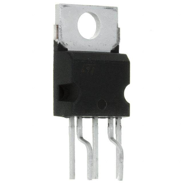
ICGOO在线商城 > 集成电路(IC) > PMIC - AC-DC 转换器,离线开关 > UCC28740D

 Datasheet下载
- 型号: UCC28740D
- 制造商: Texas Instruments
- 库位|库存: xxxx|xxxx
- 要求:
| 数量阶梯 | 香港交货 | 国内含税 |
| +xxxx | $xxxx | ¥xxxx |
查看当月历史价格
查看今年历史价格
UCC28740D产品简介:
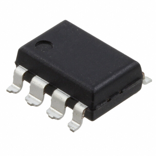
ICGOO电子元器件商城为您提供UCC28740D由Texas Instruments设计生产,在icgoo商城现货销售,并且可以通过原厂、代理商等渠道进行代购。 UCC28740D价格参考¥3.51-¥4.76。Texas InstrumentsUCC28740D封装/规格:PMIC - AC-DC 转换器,离线开关, Converter Offline Flyback Topology 170Hz ~ 100kHz 7-SOIC。您可以下载UCC28740D参考资料、Datasheet数据手册功能说明书,资料中有UCC28740D 详细功能的应用电路图电压和使用方法及教程。
UCC28740D 是 Texas Instruments 生产的一款 PMIC(电源管理集成电路),专门用于 AC-DC 转换器中的离线开关应用。该器件适用于多种应用场景,特别是在需要高效、可靠且紧凑的电源解决方案的场合。

 应用场景:

1. 消费电子设备:
   - UCC28740D 可用于电视、显示器、音频设备等消费类电子产品中,为这些设备提供稳定的直流电源。它能够处理宽范围的交流输入电压,确保在全球不同电网条件下都能正常工作。

2. 家电产品:
   - 在洗衣机、空调、冰箱等家用电器中,UCC28740D 可以作为主电源转换器,将市电转换为适合内部电路工作的直流电压。其高效率和低待机功耗特性有助于满足日益严格的能效标准。

3. 工业控制与自动化:
   - 该器件适用于工业控制系统中的电源模块,如PLC(可编程逻辑控制器)、传感器接口和电机驱动器等。UCC28740D 的高可靠性设计使其能够在恶劣的工业环境中长期稳定运行。

4. 通信设备:
   - 在路由器、交换机、基站等通信设备中,UCC28740D 可以为这些设备提供稳定的电源支持。其高效的功率转换能力有助于减少散热需求,提升系统的整体性能。

5. LED 照明系统:
   - 对于 LED 驱动电源,UCC28740D 可以实现高效的功率因数校正(PFC)和恒流输出,确保 LED 灯具在不同负载条件下的亮度一致性和长寿命。

6. 医疗设备:
   - 在便携式或固定式的医疗设备中,UCC28740D 可以为设备提供可靠的电源供应,确保设备在关键操作中的稳定性。其低电磁干扰(EMI)特性也有助于减少对其他医疗仪器的干扰。

 特点与优势:
- 高效功率转换:UCC28740D 具有较高的转换效率,能够减少能量损耗,降低发热。
- 宽输入电压范围:支持全球范围内的交流输入电压,适应性强。
- 低待机功耗:符合现代设备对节能的要求,有助于延长电池寿命或减少能耗。
- 集成保护功能:内置过压、过流、短路等多种保护机制,提高系统的安全性和可靠性。

总之,UCC28740D 凭借其高性能和多功能性,广泛应用于各种需要高效、可靠电源转换的场景中。
| 参数 | 数值 |
| 产品目录 | 集成电路 (IC)半导体 |
| 描述 | IC REG CTRLR FLYBK ISO 7SOIC开关控制器 Constant-VTG-Crnt Flyback Cntlr |
| 产品分类 | |
| 品牌 | Texas Instruments |
| 产品手册 | |
| 产品图片 | |
| 产品系列 | 电源管理 IC,开关控制器 ,Texas Instruments UCC28740D- |
| 数据手册 | |
| 产品型号 | UCC28740D |
| rohs | 无铅 / 符合限制有害物质指令(RoHS)规范要求 |
| 产品种类 | 开关控制器 |
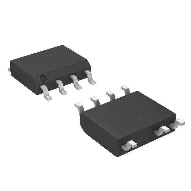
| 供应商器件封装 | 7-SOIC |
| 其它名称 | 296-36516-5 |
| 功率(W) | - |
| 包装 | 管件 |
| 占空比-最大 | 99 % |
| 商标 | Texas Instruments |
| 安装风格 | SMD/SMT |
| 封装 | Tube |
| 封装/外壳 | 8-SOIC(0.154",3.90mm 宽)7 引线 |
| 封装/箱体 | SOIC-7 |
| 工作温度 | -20°C ~ 125°C |
| 工作电源电压 | 8.1 V to 35 V |
| 工厂包装数量 | 75 |
| 开关频率 | 0.17 kHz to 100 kHz |
| 拓扑结构 | Flyback |
| 最大工作温度 | + 125 C |
| 最小工作温度 | - 40 C |
| 标准包装 | 75 |
| 电压-击穿 | - |
| 电压-输入 | 9 V ~ 35 V |
| 电压-输出 | 14V |
| 类型 | Current Mode PWM Controllers |
| 系列 | UCC28740 |
| 输出隔离 | 隔离 |
| 频率范围 | 140Hz ~ 106kHz |


- 商务部:美国ITC正式对集成电路等产品启动337调查
- 曝三星4nm工艺存在良率问题 高通将骁龙8 Gen1或转产台积电
- 太阳诱电将投资9.5亿元在常州建新厂生产MLCC 预计2023年完工
- 英特尔发布欧洲新工厂建设计划 深化IDM 2.0 战略
- 台积电先进制程称霸业界 有大客户加持明年业绩稳了
- 达到5530亿美元!SIA预计今年全球半导体销售额将创下新高
- 英特尔拟将自动驾驶子公司Mobileye上市 估值或超500亿美元
- 三星加码芯片和SET,合并消费电子和移动部门,撤换高东真等 CEO
- 三星电子宣布重大人事变动 还合并消费电子和移动部门
- 海关总署:前11个月进口集成电路产品价值2.52万亿元 增长14.8%


PDF Datasheet 数据手册内容提取
Product Order Technical Tools & Support & Folder Now Documents Software Community UCC28740 SLUSBF3D–JULY2013–REVISEDMARCH2018 UCC28740 Constant-Voltage Constant-Current Flyback Controller Using Optocoupled Feedback 1 Features 3 Description • Lessthan10-mWNo-LoadPowerCapability The UCC28740 isolated-flyback power-supply 1 controller provides Constant-Voltage (CV) using an • OptocoupledFeedbackforCV,and opticalcouplertoimprovetransientresponsetolarge- Primary-SideRegulation(PSR)forCC load steps. Constant-Current (CC) regulation is • Enables±1%VoltageRegulationand±5% accomplishedthroughPrimary-SideRegulation(PSR) CurrentRegulationAcrossLineandLoad techniques. This device processes information from opto-coupled feedback and an auxiliary flyback • 700-VStartupSwitch winding for precise high-performance control of • 100-kHzMaximumSwitchingFrequencyEnables outputvoltageandcurrent. High-Power-DensityChargerDesigns An internal 700-V startup switch, dynamically • Resonant-RingValley-SwitchingOperationfor controlled operating states, and a tailored modulation HighestOverallEfficiency profile support ultra-low standby power without • FrequencyDitheringtoEaseEMICompliance sacrificingstartuptimeoroutputtransientresponse. • ClampedGate-DriveOutputforMOSFET Control algorithms in the UCC28740 allow operating • Overvoltage,Low-Line,andOvercurrent efficiencies to meet or exceed applicable standards. ProtectionFunctions The drive output interfaces to a MOSFET power switch. Discontinuous conduction mode (DCM) with • SOIC-7Package valley-switching reduces switching losses. Modulation • CreateaCustomDesignUsingtheUCC28740 of switching frequency and primary current-peak WiththeWEBENCH®PowerDesigner amplitude (FM and AM) keeps the conversion efficiencyhighacrosstheentireloadandlineranges. 2 Applications The controller has a maximum switching frequency of • USB-CompliantAdaptersandChargersfor 100 kHz and always maintains control of the peak- ConsumerElectronics primary current in the transformer. Protection features – SmartPhones keep primary and secondary component stresses in check. A minimum switching frequency of 170 Hz – TabletComputers facilitates the achievement of less than 10-mW no- – Cameras loadpower. • StandbySupplyforTVandDesktop DeviceInformation(1) • WhiteGoods PARTNUMBER PACKAGE BODYSIZE(NOM) UCC28740 SOIC(7) 4.90mm×3.91mm (1) For all available packages, see the orderable addendum at theendofthedatasheet. SimplifiedApplicationDiagram TypicalV-IDiagram VBULK VOUT + CB1 CB2 NP NS COUT VOCV – VAC 4 V ±5% UCSCO2IC8-7740 RTL V)O VAUX VDD HV age ( 3 V NA RS1 CVDD RFB1 ut Volt 2 V p ut VS DRV ZFB O RS2 CS RLC 1 V FB GND RCS RFB2 Output Current (IO) Copyright © 2017, Texas Instruments Incorporated 1 An IMPORTANT NOTICE at the end of this data sheet addresses availability, warranty, changes, use in safety-critical applications, intellectualpropertymattersandotherimportantdisclaimers.PRODUCTIONDATA.
UCC28740 SLUSBF3D–JULY2013–REVISEDMARCH2018 www.ti.com Table of Contents 1 Features.................................................................. 1 7.4 DeviceFunctionalModes........................................13 2 Applications........................................................... 1 8 ApplicationandImplementation........................ 18 3 Description............................................................. 1 8.1 ApplicationInformation............................................18 4 RevisionHistory..................................................... 2 8.2 TypicalApplication..................................................18 5 PinConfigurationandFunctions......................... 3 9 PowerSupplyRecommendations...................... 28 6 Specifications......................................................... 4 10 Layout................................................................... 28 6.1 AbsoluteMaximumRatings .....................................4 10.1 LayoutGuidelines.................................................28 6.2 ESDRatings..............................................................4 10.2 LayoutExample....................................................29 6.3 RecommendedOperatingConditions.......................4 11 DeviceandDocumentationSupport................. 30 6.4 ThermalInformation..................................................4 11.1 DeviceSupport......................................................30 6.5 ElectricalCharacteristics...........................................5 11.2 DocumentationSupport........................................32 6.6 SwitchingCharacteristics..........................................6 11.3 ReceivingNotificationofDocumentationUpdates32 6.7 TypicalCharacteristics..............................................7 11.4 CommunityResources..........................................32 7 DetailedDescription.............................................. 9 11.5 Trademarks...........................................................33 7.1 Overview...................................................................9 11.6 ElectrostaticDischargeCaution............................33 7.2 FunctionalBlockDiagram.........................................9 11.7 Glossary................................................................33 7.3 FeatureDescription.................................................10 12 Mechanical,Packaging,andOrderable Information........................................................... 33 4 Revision History NOTE:Pagenumbersforpreviousrevisionsmaydifferfrompagenumbersinthecurrentversion. ChangesfromRevisionC(July2017)toRevisionD Page • ChangedPin7toPin8tomatchthemechanicaldrawing.................................................................................................... 3 • ChangedLayoutExample'spin7topin8tomatchthemechanicaldrawing...................................................................... 29 ChangesfromRevisionB(December2014)toRevisionC Page • MovedthetimingparametersfromtheElectricalCharacteristicstabletotheSwitchingCharacteristicstable ....................6 • Deletedquasifromquasi-resonantintheTransformerTurnsRatio,Inductance,Primary-PeakCurrentsection ..............21 • AddedtheDevelopmentSupport,DocumentationSupport,ReceivingNotificationofDocumentationUpdates,and CommunityResourcessections........................................................................................................................................... 30 ChangesfromRevisionA(July2013)toRevisionB Page • AddedESDRatingstable,FeatureDescriptionsection,DeviceFunctionalModes,ApplicationandImplementation section,PowerSupplyRecommendationssection,Layoutsection,DeviceandDocumentationSupportsection,and Mechanical,Packaging,andOrderableInformationsection ................................................................................................. 1 ChangesfromOriginal(July2013)toRevisionA Page • ChangedmarketingstatusfromProductPreviewtoProductionData .................................................................................. 1 2 SubmitDocumentationFeedback Copyright©2013–2018,TexasInstrumentsIncorporated ProductFolderLinks:UCC28740
UCC28740 www.ti.com SLUSBF3D–JULY2013–REVISEDMARCH2018 5 Pin Configuration and Functions DPackage 7-PinSOIC TopView VDD 1 8 HV VS 2 FB 3 6 DRV GND 4 5 CS PinFunctions PIN I/O DESCRIPTION NAME NO. Thecurrent-sense(CS)inputconnectstoaground-referencedcurrent-senseresistorinserieswiththepower CS 5 I switch.Theresultingvoltagemonitorsandcontrolsthepeakprimarycurrent.Aseriesresistorisaddedtothis pintocompensateforpeakswitch-currentlevelsastheAC-mainsinputvaries. DRV 6 O Drive(DRV)isanoutputthatdrivesthegateofanexternalhigh-voltageMOSFETswitchingtransistor. Thefeedback(FB)inputreceivesacurrentsignalfromtheoptocoupleroutputtransistor.Aninternalcurrent mirrordividesthefeedbackcurrentby2.5andappliesittoaninternalpullupresistortogenerateacontrol FB 3 I voltage,V .Thevoltageatthisresistordirectlydrivesthecontrollawfunction,whichdeterminestheswitching CL frequencyandthepeakamplitudeoftheswitchingcurrent. Theground(GND)pinisboththereferencepinforthecontroller,andthelow-sidereturnforthedriveoutput. GND 4 — SpecialcaremustbetakentoreturnallAC-decouplingcapacitorsascloseaspossibletothispinandavoidany commontracelengthwithanalogsignal-returnpaths. Thehigh-voltage(HV)pinmayconnectdirectly,orthroughaseriesresistor,totherectifiedbulkvoltageand HV 8 I providesachargetotheVDDcapacitorforthestartupofthepowersupply. VDDisthebias-supplyinputpintothecontroller.AcarefullyplacedbypasscapacitortoGNDisrequiredonthis VDD 1 I pin. Voltagesense(VS)isaninputusedtoprovidedemagnetizationtimingfeedbacktothecontrollertolimit frequency,tocontrolconstant-currentoperation,andtoprovideoutput-overvoltagedetection.VSisalsousedfor VS 2 I AC-mainsinput-voltagedetectionforpeakprimary-currentcompensation.Thispinconnectstoavoltagedivider betweenanauxiliarywindingandGND.ThevalueoftheupperresistorofthisdividerprogramstheAC-mains runandstopthresholds,andfactorsintolinecompensationattheCSpin. Copyright©2013–2018,TexasInstrumentsIncorporated SubmitDocumentationFeedback 3 ProductFolderLinks:UCC28740
UCC28740 SLUSBF3D–JULY2013–REVISEDMARCH2018 www.ti.com 6 Specifications 6.1 Absolute Maximum Ratings See (1)and (2). MIN MAX UNIT V Start-uppinvoltage,HV 700 V HV V Biassupplyvoltage,VDD 38 V VDD I Continuousgate-currentsink 50 mA DRV I Continuousgate-currentsource Self-limiting mA DRV I Peakcurrent,VS 1 mA FB I Peakcurrent,FB −1.2 mA VS V Gate-drivevoltageatDRV –0.5 Self-limiting V DRV Voltage,CS –0.5 5 V Voltage,FB –0.5 7 V Voltage,VS –0.75 7 V T Operatingjunctiontemperature –55 150 °C J T Storagetemperature –65 150 °C stg (1) StressesbeyondthoselistedunderAbsoluteMaximumRatingsmaycausepermanentdamagetothedevice.Thesearestressratings onlyandfunctionaloperationofthedeviceattheseoranyotherconditionsbeyondthoseindicatedunderRecommendedOperating Conditionsisnotimplied.Exposuretoabsolute-maximum-ratedconditionsforextendedperiodsmayaffectdevicereliability. (2) AllvoltagesarewithrespecttoGND.Currentsarepositiveinto,negativeoutofthespecifiedterminal.Theseratingsapplyoverthe operatingambienttemperaturerangesunlessotherwisenoted. 6.2 ESD Ratings VALUE UNIT Electrostatic Human-bodymodel(HBM),perANSI/ESDA/JEDECJS-001(1) ±2000 V V (ESD) discharge Charged-devicemodel(CDM),perJEDECspecificationJESD22-C101(2) ±500 (1) JEDECdocumentJEP155statesthat500-VHBMallowssafemanufacturingwithastandardESDcontrolprocess. (2) JEDECdocumentJEP157statesthat250-VCDMallowssafemanufacturingwithastandardESDcontrolprocess. 6.3 Recommended Operating Conditions overoperatingfree-airtemperaturerange(unlessotherwisenoted) MIN MAX UNIT V Bias-supplyoperatingvoltage 9 35 V VDD C VDDbypasscapacitor 0.047 µF VDD I Feedbackcurrent,continuous 50 µA FB I VSpincurrent,outofpin 1 mA VS T Operatingjunctiontemperature –40 125 °C J 6.4 Thermal Information UCC28740 THERMALMETRIC(1) D(SOIC) UNIT 7PINS R Junction-to-ambientthermalresistance 141.5 °C/W θJA R Junction-to-case(top)thermalresistance 73.8 °C/W θJC(top) R Junction-to-boardthermalresistance 89 °C/W θJB ψ Junction-to-topcharacterizationparameter 23.5 °C/W JT ψ Junction-to-boardcharacterizationparameter 88.2 °C/W JB (1) Formoreinformationabouttraditionalandnewthermalmetrics,seetheSemiconductorandICPackageThermalMetricsapplication report. 4 SubmitDocumentationFeedback Copyright©2013–2018,TexasInstrumentsIncorporated ProductFolderLinks:UCC28740
UCC28740 www.ti.com SLUSBF3D–JULY2013–REVISEDMARCH2018 6.5 Electrical Characteristics overoperatingfree-airtemperaturerange,V =25V,HV=open,V =0V,V =4V,T =–40°Cto+125°C,T =T VDD FB VS A J A (unlessotherwisenoted) PARAMETER TESTCONDITIONS MIN TYP MAX UNIT HIGH-VOLTAGESTARTUP I Start-upcurrentoutofVDD V =100V,V =0V,startstate 100 250 500 µA HV HV VDD I LeakagecurrentatHV V =400V,runstate,T =25°C 0.01 0.5 µA HVLKG25 HV J BIASSUPPLYINPUT I Supplycurrent,run I =0,runstate 2 2.65 mA RUN DRV I Supplycurrent,wait I =0,waitstate 95 125 µA WAIT DRV I Supplycurrent,start I =0,V =18V,startstate,I =0 18 30 µA START DRV VDD HV I Supplycurrent,fault I =0,faultstate 95 130 µA FAULT DRV UNDERVOLTAGELOCKOUT V VDDturnonthreshold V lowtohigh 19 21 23 V VDD(on) VDD V VDDturnoffthreshold V hightolow 7.35 7.75 8.15 V VDD(off) VDD VSINPUT V Negativeclamplevel I =–300µA,voltsbelowground 190 250 325 mV VSNC VSLS I Inputbiascurrent V =4V –0.25 0 0.25 µA VSB VS FBINPUT I Full-rangeinputcurrent f =f 16 23 30 µA FBMAX SW SW(min) V Inputvoltageatfullrange I =25µA,T =25°C 0.75 0.88 1 V FBMAX FB J ΔI =20µA,centeredatI =15µA,T = R FB-inputresistance,linearized FB FB J 10 14 18 kΩ FB 25°C CSINPUT V MaximumCSthresholdvoltage I =0µA(1) 738 773 810 mV CST(max) FB V MinimumCSthresholdvoltage I =35µA(1) 170 194 215 mV CST(min) FB K AM-controlratio V /V 3.6 4 4.45 V/V AM CST(max) CST(min) V Constant-currentregulationfactor 318 330 343 mV CCR K Line-compensationcurrentratio I =–300µA,I /currentoutofCSpin 24 25 28.6 A/A LC VSLS VSLS t Leading-edgeblankingtime DRVoutputduration,V =1V 180 230 280 ns CSLEB CS DRIVERS I DRVsourcecurrent V =8V,V =9V 20 25 mA DRS DRV VDD R DRVlow-sidedriveresistance I =10mA 6 12 Ω DRVLS DRV V DRVclampvoltage V =35V 14 16 V DRCL VDD R DRVpulldowninstart-state 150 190 230 kΩ DRVSS PROTECTION V Overvoltagethreshold AtVSinput,T =25°C(2) 4.52 4.6 4.71 V OVP J V Overcurrentthreshold AtCSinput 1.4 1.5 1.6 V OCP I VSline-senseruncurrent CurrentoutofVSpinincreasing 190 225 275 µA VSL(run) I VSline-sensestopcurrent CurrentoutofVSpindecreasing 70 80 100 µA VSL(stop) K VSlinesenseratio I /I 2.45 2.8 3.05 A/A VSL VSL(run) VSL(stop) T Thermal-shutdowntemperature Internaljunctiontemperature 165 °C J(stop) (1) ThisdeviceautomaticallyvariesthecontrolfrequencyandcurrentsensethresholdstoimproveEMIperformance.Thesethreshold voltagesandfrequencylimitsrepresentaveragelevels. (2) TheovervoltagethresholdlevelatVSdecreaseswithincreasingtemperatureby0.8mV/°C.Thiscompensationisincludedtoreducethe power-supplyoutputovervoltagedetectionvarianceovertemperature. Copyright©2013–2018,TexasInstrumentsIncorporated SubmitDocumentationFeedback 5 ProductFolderLinks:UCC28740
UCC28740 SLUSBF3D–JULY2013–REVISEDMARCH2018 www.ti.com 6.6 Switching Characteristics overoperatingfree-airtemperaturerange,V =25V,HV=open,V =0V,V =4V,T =–40°Cto+125°C,T =T VDD FB VS A J A (unlessotherwisenoted) PARAMETER TESTCONDITIONS MIN TYP MAX UNIT f Maximumswitchingfrequency I =0µA(1) 91 100 106 kHz SW(max) FB f Minimumswitchingfrequency I =35µA(1) 140 170 210 Hz SW(min) FB t Zero-crossingtimeoutdelay 1.8 2.1 2.55 µs ZTO (1) ThisdeviceautomaticallyvariesthecontrolfrequencyandcurrentsensethresholdstoimproveEMIperformance.Thesethreshold voltagesandfrequencylimitsrepresentaveragelevels. 6 SubmitDocumentationFeedback Copyright©2013–2018,TexasInstrumentsIncorporated ProductFolderLinks:UCC28740
UCC28740 www.ti.com SLUSBF3D–JULY2013–REVISEDMARCH2018 6.7 Typical Characteristics V =25V,T =25°C,unlessotherwisenoted. VDD J 10 10 HV = Open HV = Open Run State IRUN, VDD = 25 V 1 1 mA) mA) Current ( 0.1 Wait State Current ( 0.1 IWAIT, VDD = 25 V I - Bias-Supply VDD 0.01 VDDS Ttaurrtn S-Otaftfe VDD Turn-On I - Bias-Supply VDD 0.01 ISTART, VDD = 18 V 0.001 0.001 0.0001 0.0001 0 5 10 15 20 25 30 35 -50 -25 0 25 50 75 100 125 VDD - Bias-Supply Voltage (V) TJ - Temperature (oC) C001 C002 HV=Open HV=Open Figure1. Bias-SupplyCurrentvs.Bias-SupplyVoltage Figure2. Bias-SupplyCurrentvs.Temperature 320 300 VHV = 100 V, VVDD = 0 V 280 250 Current (µA) 220400 Current (µA) 200 IVSL(run) I - HV Startup HV 11268000 VS Line-Sense 110500 IVSL(stop) 50 40 0 0 -50 -25 0 25 50 75 100 125 -50 -25 0 25 50 75 100 125 TJ - Temperature (oC) TJ - Temperature (oC) C003 C004 V =100V,V =0V HV VDD Figure3. HVStartupCurrentvs.Temperature Figure4. VSLine-SenseCurrentsvs.Temperature 210 350 V - Minimum CS Threshold Voltage (mV) CST(min) 111112278899005050505 V - Constant-Current Regulation Factor (mV) CCR333333312233445050505 170 310 -50 -25 0 25 50 75 100 125 -50 -25 0 25 50 75 100 125 TJ - Temperature (oC) TJ - Temperature (oC) C005 C006 Figure5. MinimumCSThresholdvs.Temperature Figure6. Constant-CurrentRegulationFactorvs. Temperature Copyright©2013–2018,TexasInstrumentsIncorporated SubmitDocumentationFeedback 7 ProductFolderLinks:UCC28740
UCC28740 SLUSBF3D–JULY2013–REVISEDMARCH2018 www.ti.com Typical Characteristics (continued) V =25V,T =25°C,unlessotherwisenoted. VDD J 200 34 VDRV = 8 V, VVDD = 9 V Hz) 190 32 mum Switching Frequency ( 117800 RV Source Current (mA) 223680 f - MiniSW(min)115600 I - DDRS 2224 140 20 -50 -25 0 25 50 75 100 125 -50 -25 0 25 50 75 100 125 TJ - Temperature (oC) TJ - Temperature (oC) C007 C008 V =8V,V =9V DRV VDD Figure7. MinimumSwitchingFrequencyvs.Temperature Figure8. DRVSourceCurrentvs.Temperature 1.0 4.68 0.9 4.66 V - FB Input Voltage (V) FB 0000000.......2345678 V - VS Overvoltage Threshold (V) OVP 44444.....5566668024 4.54 0.1 0.0 4.52 0 5 10 15 20 25 30 35 -50 -25 0 25 50 75 100 125 IFB - FB Input Current (µA) TJ - Temperature (oC) C009 C010 Figure9. FBInputVoltagevs.FBInputCurrent Figure10. VSOvervoltageThresholdvs.Temperature 8 SubmitDocumentationFeedback Copyright©2013–2018,TexasInstrumentsIncorporated ProductFolderLinks:UCC28740
UCC28740 www.ti.com SLUSBF3D–JULY2013–REVISEDMARCH2018 7 Detailed Description 7.1 Overview TheUCC28740isaflybackpower-supplycontrollerwhichprovideshigh-performancevoltageregulationusingan optically coupled feedback signal from a secondary-side voltage regulator. The device provides accurate constant-current regulation using primary-side feedback. The controller operates in discontinuous-conduction mode (DCM) with valley-switching to minimize switching losses. The control law scheme combines frequency with primary peak-current amplitude modulation to provide high conversion efficiency across the load range. The control law provides a wide dynamic operating range of output power which allows the power-supply designer to easilyachievelessthan30-mWstandbypowerdissipationusingastandardshunt-regulatorandoptocoupler.For a target of less than 10-mW standby power, careful loss-management design with a low-power regulator and high-CTRoptocouplerisrequired. During low-power operating conditions, the power-management features of the controller reduce the device- operating current at switching frequencies below 32 kHz. At and above this frequency, the UCC28740 includes features in the modulator to reduce the EMI peak energy of the fundamental switching frequency and harmonics. A complete low-cost and low component-count charger-solution is realized using a straight-forward design process. 7.2 Functional Block Diagram GND IHV HV VDD POWER OC Fault UVLO AND FAULT OV Fault 21 V / 7.75 V MANAGEMENT 5 V LINE Fault FB IFB 480 k(cid:13) 5 V 14 k(cid:13) VDD 0.55 V IFB / 2.5 VCL COLNATWROL VCST 25 mA DRV VS SAMPLER + 14 V 190 k(cid:13) – OV Fault 1 / fSW VOVP VALLEY S Q SWITCHING CS R Q SECONDARY CURRENT + TIMING REGULATION DETECT – VCST LEB IVSLS LINE SENSE IVSLS – IVSLS / KLC + 10 k(cid:13) + LINE Fault OC Fault – 1.5 V 2.25 V / 0.8 V Copyright © 2017, Texas Instruments Incorporated Copyright©2013–2018,TexasInstrumentsIncorporated SubmitDocumentationFeedback 9 ProductFolderLinks:UCC28740
UCC28740 SLUSBF3D–JULY2013–REVISEDMARCH2018 www.ti.com 7.3 Feature Description 7.3.1 DetailedPinDescription VDD(DeviceBiasVoltageSupply) TheVDDpinconnectstoabypasscapacitor-to-ground.TheturnonUVLO thresholdis21VandturnoffUVLOthresholdis7.75Vwithanavailableoperatingrangeupto35V onVDD.ThetypicalUSB-chargingspecificationrequirestheoutputcurrenttooperateinconstant- currentmodefrom5Vdowntoatleast2VwhichisachievedeasilywithanominalV of VDD approximately25V.TheadditionalVDDheadroomupto35VallowsforV toriseduetothe VDD leakageenergydeliveredtotheVDDcapacitorduringhigh-loadconditions. GND(Ground) UCC28740hasasinglegroundreferenceexternaltothedeviceforthegate-drivecurrentand analogsignalreference.PlacetheVDD-bypasscapacitorclosetoGNDandVDDwithshorttraces tominimizenoiseontheVS,FB,andCSsignalpins. HV(High-VoltageStartup) TheHVpinconnectsdirectlytothebulkcapacitortoprovideastartupcurrenttothe VDDcapacitor.Thetypicalstartupcurrentisapproximately250 µAwhichprovidesfastchargingof theVDDcapacitor.TheinternalHVstartupdeviceisactiveuntilV exceedstheturnonUVLO VDD thresholdof21VatwhichtimetheHVstartupdeviceturnsoff.IntheoffstatetheHVleakage currentisverylowtominimizestandbylossesofthecontroller.WhenV fallsbelowthe7.75V VDD UVLOturnoffthresholdtheHVstartupdeviceturnson. VS(VoltageSense) TheVSpinconnectstoaresistor-dividerfromtheauxiliarywindingtoground.Theauxiliary voltagewaveformissampledattheendofthetransformersecondary-currentdemagnetizationtime toprovideaccuratecontroloftheoutputcurrentwheninconstant-currentmode.Thewaveformon theVSpindeterminesthetiminginformationtoachievevalley-switching,andthetimingtocontrol theduty-cycleofthetransformersecondarycurrent.Avoidplacingafiltercapacitoronthisinput whichinterfereswithaccuratesensingofthiswaveform. DuringtheMOSFETon-time,thispinalsosensesVScurrentgeneratedthroughR bythe S1 reflectedbulk-capacitorvoltagetoprovideforAC-inputrunandstopthresholds,andtocompensate thecurrent-sensethresholdacrosstheAC-inputrange.FortheAC-inputrun/stopfunction,therun thresholdonVSis225µAandthestopthresholdis80 µA. Attheendofoff-timedemagnetization,thereflectedoutputvoltageissampledatthispintoprovide outputovervoltageprotection.Thevaluesfortheauxiliaryvoltage-dividerupper-resistor,R ,and S1 lower-resistor,R ,aredeterminedbyEquation1andEquation2. S2 V ´ 2 R = IN(run) S1 N ´I PA VSL(run) where • N isthetransformerprimary-to-auxiliaryturns-ratio, PA • V istheACRMSvoltagetoenableturnonofthecontroller(run), IN(run) (incaseofDCinput,leaveoutthe√2termintheequation), • I istherun-thresholdforthecurrentpulledoutoftheVSpinduringtheswitchon-time(seeElectrical VSL(run) Characteristics). (1) R uV R S1 OVP S2 N u(cid:11)V (cid:16)V (cid:12)(cid:16)V AS OV F OVP where • V isthemaximumallowablepeakvoltageattheconverteroutput, OV • V istheoutput-rectifierforwarddropatnear-zerocurrent, F • N isthetransformerauxiliary-to-secondaryturns-ratio, AS • R istheVSdividerhigh-sideresistance, S1 • V istheovervoltagedetectionthresholdattheVSinput(seeElectricalCharacteristics). (2) OVP FB(Feedback) TheFBpinconnectstotheemitterofananalog-optocoupleroutputtransistorwhichusuallyhas thecollectorconnectedtoVDD.ThecurrentsuppliedtoFBbytheoptocouplerisreducedinternally byafactorof2.5andtheresultingcurrentisappliedtoaninternal480-kΩ resistortogeneratethe controllawvoltage(V ).ThisV directlydeterminestheconverterswitchingfrequencyandpeak CL CL primarycurrentrequiredforregulationperthecontrol-lawforanygivenlineandloadcondition. 10 SubmitDocumentationFeedback Copyright©2013–2018,TexasInstrumentsIncorporated ProductFolderLinks:UCC28740
UCC28740 www.ti.com SLUSBF3D–JULY2013–REVISEDMARCH2018 Feature Description (continued) DRV(GateDrive) TheDRVpinconnectstotheMOSFETgatepin,usuallythroughaseriesresistor.Thegate driverprovidesagate-drivesignallimitedto14V.Theturnoncharacteristicofthedriverisa25-mA currentsourcewhichlimitstheturnondv/dtoftheMOSFETdrainandreducestheleading-edge currentspikewhilestillprovidingagate-drivecurrenttoovercometheMillerplateau.Thegate-drive turnoffcurrentisdeterminedbytheR ofthelow-sidedriveralongwithanyexternalgate-drive DSON resistance.AddingexternalgateresistancereducestheMOSFETdrainturn-offdv/dt,ifnecessary. CS(CurrentSense) Thecurrent-sensepinconnectsthroughaseriesresistor(R )tothecurrent-senseresistor LC (R ).Themaximumcurrent-sensethreshold(V )is0.773VforI ,andtheminimum CS CST(max) PP(max) current-sensethreshold(V )is0.194VforI .R providesthefeed-forwardline CST(min) PP(min) LC compensationtoeliminatechangesinI withinputvoltageduetothepropagationdelayofthe PP internalcomparatorandMOSFETturnofftime.Aninternalleading-edgeblankingtimeof235ns eliminatessensitivitytotheMOSFETturnoncurrentspike.PlacingabypasscapacitorontheCS pinisunnecessary.Thetargetoutputcurrentinconstant-current(CC)regulationdeterminesthe valueofR .ThevaluesofR andR arecalculatedusingEquation3andEquation4.Theterm CS CS LC V istheproductofthedemagnetizationconstant,0.425,andV .V isheldtoatighter CCR CST(max) CCR accuracythaneitherofitsconstituentterms.Theterm η accountsfortheenergystoredinthe XFMR transformerbutnotdeliveredtothesecondary.Thistermincludestransformerresistanceandcore loss,biaspower,andprimary-to-secondaryleakageratio. Example: With a transformer core and winding loss of 5%, primary-to-secondary leakage inductance of 3.5%, and bias power to output power ratio of 0.5%, the η value at full power is approximately: 1 - 0.05 - 0.035 - 0.005 = XFMR 0.91. RCS = VCCR´NPS ´ hXFMR 2I OCC where • V isaconstant-currentregulationfactor(seeElectricalCharacteristics), CCR • N isthetransformerprimary-to-secondaryturns-ratio(aratioof13to15istypicalfor5-Voutput), PS • I isthetargetoutputcurrentinconstant-currentregulation, OCC • η isthetransformerefficiencyatfullpower. (3) XFMR K ´R ´R ´t ´N R = LC S1 CS D PA LC L P where • R istheVSpinhigh-sideresistorvalue, S1 • R isthecurrent-senseresistorvalue, CS • t isthetotalcurrent-sensedelayconsistingofMOSFETturnoffdelay,plusapproximately50nsinternaldelay, D • N isthetransformerprimary-to-auxiliaryturns-ratio, PA • L isthetransformerprimaryinductance, P • K isacurrent-scalingconstantforlinecompensation(seeElectricalCharacteristics). (4) LC 7.3.2 Valley-SwitchingandValley-Skipping The UCC28740 uses valley-switching to reduce switching losses in the MOSFET, to reduce induced-EMI, and to minimize the turnon current spike at the current-sense resistor. The controller operates in valley-switching in all loadconditionsunlesstheV ringingdiminishestothepointwherevalleysarenolongerdetectable. DS As shown in Figure 11, the UCC28740 operates in a valley-skipping mode (also known as valley-hopping) in most load conditions to maintain an accurate voltage or current regulation point and still switch on the lowest availableV voltage. DS Copyright©2013–2018,TexasInstrumentsIncorporated SubmitDocumentationFeedback 11 ProductFolderLinks:UCC28740
UCC28740 SLUSBF3D–JULY2013–REVISEDMARCH2018 www.ti.com Feature Description (continued) VDS VDRV Figure11. Valley-SkippingMode Valley-skipping modulates each switching cycle into discrete period durations. During FM operation, the switching cycles are periods when energy is delivered to the output in fixed packets, where the power-per-cycle varies discretely with the switching period. During operating conditions when the switching period is relatively short, such as at high-load and low-line, the average power delivered per cycle varies significantly based on the number of valleys skipped between cycles. As a consequence, valley-skipping adds additional ripple voltage to the output with a frequency and amplitude dependent upon the loop-response of the shunt-regulator. For a load with an average power level between that of cycles with fewer valleys skipped and cycles with more valleys skipped, the voltage-control loop modulates the FB current according to the loop-bandwidth and toggles between longerandshorterswitchingperiodstomatchtherequiredaverageoutputpower. 7.3.3 StartupOperation An internal high-voltage startup switch, connected to the bulk-capacitor voltage (V ) through the HV pin, BULK charges the VDD capacitor. This startup switch functions similarly to a current source providing typically 250 µA to charge the VDD capacitor. When V reaches the 21-V UVLO turnon threshold the controller is enabled, the VDD converterstartsswitching,andthestartupswitchturnsoff. Often at initial turnon, the output capacitor is in a fully discharged state. The first three switching-cycle current peaks are limited to I to monitor for any initial input or output faults with limited power delivery. After these PP(min) three cycles, if the sampled voltage at VS is less than 1.33 V, the controller operates in a special startup mode. In this mode, the primary current peak amplitude of each switching cycle is limited to approximately 0.63 × I and D increases from 0.425 to 0.735. These modifications to I and D during startup PP(max) MAGCC PP(max) MAGCC allows high-frequency charge-up of the output capacitor to avoid audible noise while the demagnetization voltage is low. Once the sampled VS voltage exceeds 1.38 V, D is restored to 0.425 and the primary current peak MAGCC resumes as I . While the output capacitor charges, the converter operates in CC mode to maintain a PP(max) constant output current until the output voltage enters regulation. Thereafter, the controller responds to the condition dictated by the control law. The time to reach output regulation consists of the time the VDD capacitor chargesto21Vplusthetimetheoutputcapacitorcharges. 7.3.4 FaultProtection TheUCC28740providesextensivefaultprotection.Theprotectionfunctionsinclude: • Outputovervoltage • Inputundervoltage • Internalovertemperature • Primaryovercurrentfault • CS-pinfault • VS-pinfault AUVLOresetandrestartsequenceappliestoallfault-protectionevents. 12 SubmitDocumentationFeedback Copyright©2013–2018,TexasInstrumentsIncorporated ProductFolderLinks:UCC28740
UCC28740 www.ti.com SLUSBF3D–JULY2013–REVISEDMARCH2018 Feature Description (continued) Theoutput-overvoltagefunctionisdeterminedbythevoltagefeedbackontheVSpin.IfthevoltagesampleofVS exceeds 4.6 V, the device stops switching and the internal current consumption becomes I which FAULT dischargestheVDDcapacitortotheUVLO-turnoffthreshold.Afterthat,thedevicereturnstothestartstateanda startupsequenceensues. The UCC28740 always operates with cycle-by-cycle primary peak current control. The normal operating voltage range of the CS pin is 0.773 V to 0.194 V. An additional protection, not filtered by leading-edge blanking, occurs iftheCSpinvoltagereaches1.5V,whichresultsinaUVLOresetandrestartsequence. Current into the VS pin during the MOSFET on-time determines the line-input run and stop thresholds. While the VS pin clamps close to GND during the MOSFET on-time, the current through R is monitored to determine a S1 sample of V . A wide separation of the run and stop thresholds allows for clean startup and shutdown of the BULK powersupplywiththelinevoltage.Therun-currentthresholdis225 µAandthestop-currentthresholdis80µA. The internal overtemperature-protection threshold is 165°C. If the junction temperature reaches this threshold the device initiates a UVLO-reset cycle. If the temperature is still high at the end of the UVLO cycle, the protection cyclerepeats. Protection is included in the event of component failures on the VS pin. If complete loss of feedback information ontheVSpinoccurs,thecontrollerstopsswitchingandrestarts. 7.4 Device Functional Modes 7.4.1 Secondary-SideOpticallyCoupledConstant-Voltage(CV)Regulation Figure 12 shows a simplified flyback convertor with the main output-regulation blocks of the device shown, along with typical implementation of secondary-side-derived regulation. The power-train operation is the same as any DCM-flyback circuit. A feedback current is optically coupled to the controller from a shunt-regulator sensing the outputvoltage. VBULK + VF – VOUT Timing COUT Primary Secondary RLOAD Auxiliary RS1 VS Discriminator and VCL GD DRV Sampler Control Law RS2 VDD Minimum Period CS RTL and Peak Primary Current RCS Zero Crossings ROPT RFB1 Mirror Network FB IOPT ZFB IFB RFB2 Figure12. SimplifiedFlybackConvertor (WiththeMainVoltageRegulationBlocks) Copyright©2013–2018,TexasInstrumentsIncorporated SubmitDocumentationFeedback 13 ProductFolderLinks:UCC28740
UCC28740 SLUSBF3D–JULY2013–REVISEDMARCH2018 www.ti.com Device Functional Modes (continued) In this configuration, a secondary-side shunt-regulator, such as the TL431, generates a current through the input photo-diode of an optocoupler. The photo-transistor delivers a proportional current that is dependent on the current-transfer ratio (CTR) of the optocoupler to the FB input of the UCC28740 controller. This FB current then converts into the V by the input-mirror network, detailed in the device block diagram (see Functional Block CL Diagram). Output-voltage variations convert to FB-current variations. The FB-current variations modify the V CL which dictates the appropriate I and f necessary to maintain CV regulation. At the same time, the VS input PP SW senses the auxiliary winding voltage during the transfer of transformer energy to the secondary output to monitor for an output overvoltage condition. When f reaches the target maximum frequency, chosen between 32 kHz SW and100kHz,CCoperationisenteredandfurtherincreasesinV havenoeffect. CL Figure 13 shows that as the secondary current decreases to zero, a clearly defined down slope reflects the decreasingrectifierV combinedwithstrayresistancevoltage-drop(I R ).Toachieveanaccuraterepresentation F S S of the secondary output voltage on the auxiliary winding, the discriminator reliably blocks the leakage-inductance reset and ringing while continuously sampling the auxiliary voltage during the down slope after the ringing diminishes. The discriminator then captures the voltage signal at the moment that the secondary-winding current reaches zero. The internal overvoltage threshold on VS is 4.6 V. Temperature compensation of –0.8 mV/°C on the overvoltage threshold offsets the change in the output-rectifier forward voltage with temperature. The resistor dividerisselectedasoutlinedintheVSpindescription(seeDetailedPinDescription). VS Sample (VOUT+VF) NAS 0 V –VBULK / NPA Figure13. Auxiliary-WindingVoltage The UCC28740 VS-signal sampler includes signal-discrimination methods to ensure an accurate sample of the output voltage from the auxiliary winding. Controlling some details of the auxiliary-winding signal to ensure reliable operation is necessary; specifically, the reset time of the leakage inductance and the duration of any subsequent leakage-inductance ringing. See Figure 14 for a detailed illustration of waveform criteria to ensure a reliablesampleontheVSpin. The first detail to examine is the duration of the leakage-inductance reset pedestal, t , in Figure 14. LK_RESET Because t mimics the waveform of the secondary-current decay, followed by a sharp downslope, LK_RESET t is internally blanked for a duration which scales with the peak primary current. Keeping the leakage- LK_RESET resettimetolessthan600nsforI ,andlessthan2.2µsforI isimportant. PP(min) PP(max) The second detail is the amplitude of ringing on the V waveform following t . The peak-to-peak voltage AUX LK_RESET variation at the VS pin must be less than 100 mVp-p for at least 200 ns before the end of the demagnetization time (t ). A concern with excessive ringing usually occurs during light or no-load conditions, when t is at the DM DM minimum. The tolerable ripple on VS is scaled up to the auxiliary-winding voltage by R and R , and is equal to S1 S2 100mV× (R +R )/R . S1 S2 S2 14 SubmitDocumentationFeedback Copyright©2013–2018,TexasInstrumentsIncorporated ProductFolderLinks:UCC28740
UCC28740 www.ti.com SLUSBF3D–JULY2013–REVISEDMARCH2018 Device Functional Modes (continued) tLK_RESET tSMPL VS ring (p-p) 0 V tDM Figure14. Auxiliary-WindingWaveformDetails During voltage regulation, the controller operates in frequency-modulation mode and amplitude-modulation mode, as shown in Figure 15. The internal operating-frequency limits of the device are 100 kHz and f . The SW(min) maximum operating frequency of the converter at full-load is generally chosen to be slightly lower than 100 kHz to allow for tolerances, or significantly lower due to switching-loss considerations. The maximum operating frequency and primary peak current chosen determine the transformer primary inductance of the converter. The shunt-regulator bias power, output preload resistor (if any), and low-power conversion efficiency determine the minimum-operating frequency of the converter. Voltage-loop stability compensation is applied at the shunt- regulator which drives the opto-coupled feedback signal. The tolerances chosen for the shunt-regulator reference andthesenseresistorsdeterminestheregulationaccuracy. Copyright©2013–2018,TexasInstrumentsIncorporated SubmitDocumentationFeedback 15 ProductFolderLinks:UCC28740
UCC28740 SLUSBF3D–JULY2013–REVISEDMARCH2018 www.ti.com Device Functional Modes (continued) Control-Law Profile in Constant-Voltage (CV) Mode IPP(max) 100 kHz nt) e urr IPP y c SW mar f fSW pri k a e p (P P I 32 kHz IPP(max) / 4 FM AM FM fSW = 170 Hz 3 kHz 0 V 0.75 V 1.3 V 2.2 V 3.55 V 4.9 V 5 V Control Law Voltage, Internal (V ) CL 26 µA 22.1 µA 19.3 µA 14.6 µA 7.55 µA 0.5 µA Corresponding Feedback Current, FB Input (I ) FB Figure15. FrequencyandAmplitudeModulationModes (DuringCVRegulation) The level of feedback current (I ) into the FB pin determines the internal V which determines the operating FB CL point of the controller while in CV mode. When I rises above 22 µA, no further decrease in f occurs. When FB SW the output-load current increases to the point where maximum f is reached, control transfers to CC mode. All SW current, voltage, frequency, breakpoints, and curve-segment linearity depicted in Figure 15 are nominal. Figure15indicatesthegeneraloperationofthecontrollerwhileinCVmode,althoughminorvariationsmayoccur from part to part. An internal frequency-dithering mechanism is enabled when I is less than 14.6 µA to help FB reduceconductedEMI(includingduringCC-modeoperation),andisdisabledotherwise. 7.4.2 Primary-SideConstant-Current(CC)Regulation When the load current of the converter increases to the predetermined constant-current limit, operation enters CC mode. In CC mode, output voltage regulation is lost and the shunt-regulator drives the current and voltage at FB to minimum. During CC mode, timing information at the VS pin and current information at the CS pin allow accurate regulation of the average current of the secondary winding. The CV-regulation control law dictates that as load increases approaches CC regulation the primary peak current will be at I . The primary peak PP(max) current, turns-ratio, demagnetization time t , and switching period t determine the secondary average output DM SW current (see Figure 16). Ignoring leakage-inductance effects, the average output current is given by Equation 5. When the demagnetization duty-cycle reaches the CC-regulation reference, D , in the current-control block, MAGCC the controller operates in frequency modulation (FM) mode to control the output current for any output voltage at or below the voltage-regulation target as long as the auxiliary winding keeps V above the UVLO turnoff VDD threshold. As the output voltage falls, t increases. The controller acts to increase t to maintain the ratio of DM SW t to switching period (t / t ) at a maximum of 0.425 (D ), thereby maintaining a constant average DM DM SW MAGCC outputcurrent. 16 SubmitDocumentationFeedback Copyright©2013–2018,TexasInstrumentsIncorporated ProductFolderLinks:UCC28740
UCC28740 www.ti.com SLUSBF3D–JULY2013–REVISEDMARCH2018 Device Functional Modes (continued) I ´N I S S PP N P t t ON DM t SW UDG-12203 Figure16. Transformer-CurrentRelationship I N t I = PP ´ P ´ DM OUT 2 N t S SW (5) Fast, accurate, opto-coupled CV control combined with line-compensated PSR CC control results in high- performance voltage and current regulation which minimizes voltage deviations due to heavy load and unload steps,asillustratedbytheV-IcurveinFigure17. VOCV VO(min) )O V ge ( IOCC ±5% a Minimum allowable Volt transient voltage level ut for heavy load step p ut O Output Current (I ) IOCC O Figure17. TypicalTargetOutputV-ICharacteristic Copyright©2013–2018,TexasInstrumentsIncorporated SubmitDocumentationFeedback 17 ProductFolderLinks:UCC28740
UCC28740 SLUSBF3D–JULY2013–REVISEDMARCH2018 www.ti.com 8 Application and Implementation NOTE Information in the following applications sections is not part of the TI component specification, and TI does not warrant its accuracy or completeness. TI’s customers are responsible for determining suitability of components for their purposes. Customers should validateandtesttheirdesignimplementationtoconfirmsystemfunctionality. 8.1 Application Information The UCC28740 is a flyback controller that provides constant-voltage (CV) mode control and constant current (CC) mode control for precise output regulation. While in CV operating range, the controller uses an opto-coupler for tight voltage regulation and improved transient response to large load steps. Accurate regulation while in CC mode is provided by primary side control. The UCC28740 uses frequency modulation, peak primary current modulation, valley switching and valley hopping in its control algorithm in order to maximize efficiency over the entireoperatingrange. 8.2 Typical Application The UCC28740 is well suited for use in isolated off-line systems requiring high efficiency and fault protection features such as USB compliant adapters and chargers for consumer electronics such a smart phones, tablet computers,andcameras.A10-WapplicationforaUSBchargerisshowninFigure18. This procedure outlines the steps to design a constant-voltage, constant-current flyback converter using the UCC28740 controller. See Figure 18 for component names and network locations. The design procedure equationsusetermsthataredefinedbelow. VBULK + VF – VOUT + CB1 CB2 NP NS COUT – VAC UCC28740 RTL VAUX + VFA – VVDD SOIC-7 VDD HV NA RS1 CVDD ROPT VE VS DRV RFB1 RS2 CFB3 RFB3 CS RLC IOPT ZFB FB RCS GND IFB RFB4 RFB2 Copyright © 2017, Texas Instruments Incorporated Figure18. DesignProcedureApplicationExample 18 SubmitDocumentationFeedback Copyright©2013–2018,TexasInstrumentsIncorporated ProductFolderLinks:UCC28740
UCC28740 www.ti.com SLUSBF3D–JULY2013–REVISEDMARCH2018 Typical Application (continued) 8.2.1 DesignRequirements Table1.DesignParameters PARAMETER NOTESANDCONDITIONS MIN NOM MAX UNIT INPUTCHARACTERISTICS InputVoltage,V 85 115/230 265 V IN RMS MaximumInputCurrent V =V ,I =I 0.265 A IN INmin OUT OUTmax RMS LineFrequency 47 60/50 63 Hz NoLoadInputPower V ≤V ≤V ,I =0A 20 mW Consumption INmin IN INmax OUT OUTPUTCHARACTERISTICS OutputVoltage,V V ≤V ≤V ,0A≤I ≤I 4.95 5 5.05 V OUT INmin IN INmax OUT OUTmax OutputLoadCurrent,CVMode, V ≤V ≤V 1.995 2.1 2.205 A I INmin IN INmax OUTmax LineRegulation:V ≤V ≤V ,I ≤ INmin IN INmax OUT 0.1% OutputVoltageRegulation IOUTmax LoadRegulation:0A≤I ≤I 0.1% OUT OUTmax OutputVoltageRipple V ≤V ≤V ,0A≤I ≤I 150 mVpp INmin IN INmax OUT OUTmax OutputOvercurrent,I V ≤V ≤V 2.5 A CCC INmin IN INmax MinimumOutputVoltage,CC V ≤V ≤V ,I =I 1.78 2 V Mode INmin IN INmax OUT OCC Brown-outProtection I =I 68 V OUT OUTmax RMS TransientResponseUndershoot I =I to0-Aloadtransient 4.3 V OUT OUTmax TransientResponseTime I =I to0-Aloadtransient 20 ms OUT OUTmax SYSTEMSCHARACTERISTICS SwitchingFrequency,f 1.2 71 kHz SW 25%,50%,75%,100%loadaverageat AverageEfficiency 81% nominalinputvoltages OperatingTemperature 25 °C 8.2.2 DetailedDesignProcedure 8.2.2.1 CustomDesignWithWEBENCH® Tools ClickheretocreateacustomdesignusingtheUCC28740devicewiththeWEBENCH®PowerDesigner. 1. Startbyenteringtheinputvoltage(V ),outputvoltage(V ),andoutputcurrent(I )requirements. IN OUT OUT 2. Optimizethedesignforkeyparameterssuchasefficiency,footprint,andcostusingtheoptimizerdial. 3. ComparethegenerateddesignwithotherpossiblesolutionsfromTexasInstruments. The WEBENCH Power Designer provides a customized schematic along with a list of materials with real-time pricingandcomponentavailability. Inmostcases,theseactionsareavailable: • Runelectricalsimulationstoseeimportantwaveformsandcircuitperformance • Runthermalsimulationstounderstandboardthermalperformance • ExportcustomizedschematicandlayoutintopopularCADformats • PrintPDFreportsforthedesign,andsharethedesignwithcolleagues GetmoreinformationaboutWEBENCHtoolsatwww.ti.com/WEBENCH. Copyright©2013–2018,TexasInstrumentsIncorporated SubmitDocumentationFeedback 19 ProductFolderLinks:UCC28740
UCC28740 SLUSBF3D–JULY2013–REVISEDMARCH2018 www.ti.com 8.2.2.2 StandbyPowerEstimateandNo-LoadSwitchingFrequency Assuming minimal no-load standby power is a critical design requirement, determine the estimated no-load power loss based on an accounting of all no-load operating and leakage currents at their respective voltages. Close attention to detail is necessary to account for all of the sources of leakage, however, in many cases, prototype measurement is the only means to obtain a realistic estimation of total primary and secondary leakage currents. At present, converter standby power is certified by compliance-agency authorities based on steady- stateroom-temperatureoperationatthehighestnominalinputvoltagerating(typically230Vrms). Equation 6 estimates the standby power loss from the sum of all leakage currents of the primary-side components of the converter. These leakage currents are measured in aggregate by disconnecting the HV input of the controller from the bulk-voltage rail to prevent operating currents from interfering with the leakage measurement. n ƒP P V u I PRI_SB BULK PRI_LK K k 1 (6) Equation 7 estimates the standby power loss from the sum of all leakage and operating currents of the secondary-side components on the output of the converter. Leakage currents result from reverse voltage applied across the output rectifier and capacitors, while the operating current includes currents required by the shunt- regulator,optocoupler,andassociatedcomponents. n ƒS P V u I SEC_SB OCV SEC K k 1 (7) Equation 8 estimates the standby power loss from the sum of all leakage and operating currents of the auxiliary- side components on the controller of the converter. Leakage currents of the auxiliary diode and capacitor are usually negligible. The operating current includes the wait-state current, I , of the UCC28740 controller, plus WAIT the optocoupler-output current for the FB network in the steady-state no-load condition. The VDD voltage in the no-loadconditionV arethelowestpracticablevaluetominimizeloss. VDDNL n ƒa P V u I AUX_SB VDDNL AUX K k 1 (8) NotethatP istheonlylossthatisnotdependentontransformerconversionefficiency.P andP PRI_SB SEC_SB AUX_SB are processed through the transformer and incur additional losses as a consequence. Typically, the transformer no-load conversion efficiency η lies in the range of 0.50 to 0.70. Total standby input power (no-load SWNL condition)isestimatedbyEquation9. 1 (cid:11) (cid:12) P P (cid:14) P (cid:14)P SB PRI_SB SEC_SB AUX_SB K SWNL (9) Although the UCC28740 is capable of operating at the minimum switching frequency of 170 Hz, a typical converter is likely to require a higher frequency to sustain operation at no-load. An accurate estimate of the no- load switching frequency f entails a thorough accounting of all switching-related energy losses within the SWNL converter including parasitic elements of the power-train components. In general, f is likely to lie within the SWNL range of 400 Hz to 800 Hz. A more detailed treatment of standby power and no-load frequency is beyond the scopeofthisdatasheet. 8.2.2.3 InputBulkCapacitanceandMinimumBulkVoltage Determine the minimum voltage on the input bulk capacitance, C and C total, in order to determine the B1 B2 maximum Np-to-Ns turns-ratio of the transformer. The input power of the converter based on target full-load efficiency, the minimum input RMS voltage, and the minimum AC input frequency determine the input capacitancerequirement. Maximum input power is determined based on I , V , V (if used), and the full-load conversion-efficiency OCC OCV CBC target. (cid:11)V (cid:14)V (cid:12)uI P OCV CBC OCC IN K (10) 20 SubmitDocumentationFeedback Copyright©2013–2018,TexasInstrumentsIncorporated ProductFolderLinks:UCC28740
UCC28740 www.ti.com SLUSBF3D–JULY2013–REVISEDMARCH2018 Equation 11 provides an accurate solution for the total input capacitance based on a target minimum bulk- capacitor voltage. Alternatively, to target a given input capacitance value, iterate the minimum capacitor voltage toachievethetargetcapacitancevalue. 2P ´æç0.25 + 1 ´arcsinæç VBULK(min) ö÷ö÷ IN ç 2p ç 2 ´ V ÷÷ è è IN(min) øø C = BULK (2V 2 - V 2)´f IN(min) BULK(min) LINE (11) 8.2.2.4 TransformerTurns-Ratio,Inductance,PrimaryPeakCurrent The target maximum switching frequency at full-load, the minimum input-capacitor bulk voltage, and the estimatedDCMresonanttimedeterminethemaximumprimary-to-secondaryturns-ratioofthetransformer. Initially determine the maximum-available total duty-cycle of the on-time and secondary conduction time based on the target switching frequency, f , and DCM resonant time. For DCM resonant frequency, assume 500 kHz MAX if an estimate from previous designs is not available. At the transition-mode operation limit of DCM, the interval required from the end of secondary current conduction to the first valley of the V voltage is ½ of the DCM DS resonant period (t ), or 1 µs assuming 500 kHz resonant frequency. The maximum allowable MOSFET on-time R D isdeterminedusingEquation12. MAX §t • D 1(cid:16)D (cid:16)¤ R uf ‚ MAX MAGCC MAX ' 2 „ (12) When D is known, the maximum primary-to-secondary turns-ratio is determined with Equation 13. D is MAX MAGCC defined as the secondary-diode conduction duty-cycle during CC operation and is fixed internally by the UCC28740 at 0.425. The total voltage on the secondary winding must be determined, which is the sum of V , OCV V ,andV .Forthe5-VUSB-chargerapplications,aturnsratiorangeof13to15istypicallyused. F OCBC D ´ V MAX BULK(min) N = PS(max) D ´(V + V + V ) MAGCC OCV F OCBC (13) A higher turns-ratio generally improves efficiency, but may limit operation at low input voltage. Transformer design iterations are generally necessary to evaluate system-level performance trade-offs. When the optimum turns-ratioN isdeterminedfromadetailedtransformerdesign,usethisratioforthefollowingparameters. PS The UCC28740 constant-current regulation is achieved by maintaining D at the maximum primary peak MAGCC current setting. The product of D and V defines a CC-regulating voltage factor V which is used MAGCC CST(max) CCR with N to determine the current-sense resistor value necessary to achieve the regulated CC target, I (see PS OCC Equation14). Because a small portion of the energy stored in the transformer does not transfer to the output, a transformer- efficiency term is included in the R equation. This efficiency number includes the core and winding losses, the CS leakage-inductance ratio, and a bias-power to maximum-output-power ratio. An overall-transformer efficiency of 0.91 is a good estimate based on 3.5% leakage inductance, 5% core & winding loss, and 0.5% bias power, for example.Adjusttheseestimatesasappropriatebasedoneachspecificapplication. RCS = VCCR´NPS ´ hXFMR 2I OCC (14) The primary transformer inductance is calculated using the standard energy storage equation for flyback transformers.Primarycurrent,maximumswitchingfrequency,outputvoltageandcurrenttargets,andtransformer powerlossesareincludedinEquation16. First, determine the transformer primary peak current using Equation 15. Peak primary current is the maximum current-sensethresholddividedbythecurrent-senseresistance. V I = CST(max) PP(max) R CS (15) 2(V + V + V )´I OCV F OCBC OCC L = P h ´I 2 ´f XFMR PP(max) MAX (16) Copyright©2013–2018,TexasInstrumentsIncorporated SubmitDocumentationFeedback 21 ProductFolderLinks:UCC28740
UCC28740 SLUSBF3D–JULY2013–REVISEDMARCH2018 www.ti.com N is determined by the lowest target operating output voltage while in constant-current regulation and by the AS VDD UVLO turnoff threshold of the UCC28740. Additional energy is supplied to VDD from the transformer leakage-inductancewhichallowsalowerturnsratiotobeusedinmanydesigns. V (cid:14)V N VDD(off) FA AS V (cid:14)V OCC F (17) 8.2.2.5 TransformerParameterVerification Because the selected transformer turns-ratio affects the MOSFET V and the secondary and auxiliary rectifier DS reversevoltages,areviewofthesevoltagesisimportant.Inaddition,internaltimingconstraintsoftheUCC28740 require a minimum on time of the MOSFET (t ) and a minimum demagnetization time (t ) of the transformer in ON DM thehigh-lineminimum-loadcondition.Theselectionoff ,L ,andR affectstheminimumt andt . MAX P CS ON DM Equation 18 and Equation 19 determine the reverse voltage stresses on the secondary and auxiliary rectifiers. Strayinductancecanimpressadditionalvoltagespikesuponthesestressesandsnubbersmaybenecessary. V u 2 V IN(max) u V REVS OV N PS (18) V u 2 V IN(max) u V REVA VDD N PA (19) FortheMOSFETV peakvoltagestress,anestimatedleakageinductancevoltagespike(V )isincluded. DS LK V (cid:11)V u 2(cid:12)(cid:14)(cid:11)V (cid:14)V (cid:14)V (cid:12)uN (cid:14)V DSPK IN(max) OCV F OCBC PS LK (20) Equation 21 determines if t exceeds the minimum t target of 280 ns (maximum t ). Equation 22 ON(min) ON CSLEB verifiesthatt exceedstheminimumt targetof1.2 µs. DM(min) DM L I t P u PP(max) ON(min) V u 2 K IN(max) AM (21) t u V u 2 ON(min) IN(max) t DM(min) N u(cid:11)V (cid:14)V (cid:12) PS OCV F (22) 8.2.2.6 VSResistorDivider,LineCompensation The VS divider resistors determine the output overvoltage detection point of the flyback converter. The high-side divider resistor (R ) determines the input-line voltage at which the controller enables continuous DRV operation. S1 R is determined based on transformer primary-to-auxiliary turns-ratio and desired input voltage operating S1 threshold. V ´ 2 R = IN(run) S1 N ´I PA VSL(run) (23) Thelow-sideVSpinresistoristhenselectedbasedonthedesiredovervoltagelimit,V . OV R u V S1 OVP R S2 N u(cid:11)V (cid:16)V (cid:12)(cid:16)V AS OV F OVP (24) The UCC28740 maintains tight constant-current regulation over varying input line by using the line-compensation feature. The line-compensation resistor (R ) value is determined by current flowing in R and the total internal LC S1 gate-driveandexternalMOSFETturnoffdelay.Assumeaninternaldelayof50nsintheUCC28740. K ´R ´R ´t ´N R = LC S1 CS D PA LC L P (25) 22 SubmitDocumentationFeedback Copyright©2013–2018,TexasInstrumentsIncorporated ProductFolderLinks:UCC28740
UCC28740 www.ti.com SLUSBF3D–JULY2013–REVISEDMARCH2018 8.2.2.7 OutputCapacitance The output capacitance value is often determined by the transient-response requirement from the no-load condition. For example, in typical low-power USB-charger applications, there is a requirement to maintain a minimum transient V of 4.1 V with a load-step I from 0 mA to 500 mA. Yet new higher-performance O TRAN applications require smaller transient voltage droop V with I of much greater amplitude (such as from no- OΔ TRAN loadtofull-load),whichdrivestheneedforhigh-speedopto-coupledvoltagefeedback. I ut C t TRAN RESP OUT V O’ where • t isthetimedelayfromthemomentI isappliedtothemomentwhenI fallsbelow1µA (26) RESP TRAN FB Additional considerations for the selection of appropriate output capacitors include ripple-current, ESR, and ESL ratings necessary to meet reliability and ripple-voltage requirements. Detailed design criteria for these considerationsarebeyondthescopeofthisdatasheet. 8.2.2.8 VDDCapacitance,C VDD The capacitance on VDD must supply the primary-side operating current used during startup and between low- frequency switching pulses. The largest result of three independent calculations denoted in Equation 27, Equation28,andEquation29determinesthevalueofC . VDD At startup, when V is reached, C alone supplies the device operating current and MOSFET gate current VDD(on) VDD until the output of the converter reaches the target minimum-operating voltage in CC regulation, V . Now the OCC auxiliarywindingsustainsVDDfortheUCC28740aboveUVLO.Thetotaloutputcurrentavailabletotheloadand to charge the output capacitors is the CC-regulation target, I . Equation 27 assumes that all of the output OCC current of the converter is available to charge the output capacitance until V is achieved. For typical OCC applications, Equation 27includes an estimated q f of average gate-drive current and a 1-V margin added GSW(max) toV . VDD C u V (cid:11)I (cid:14)q f (cid:12)u OUT OCC RUN GSW(max) I C t OCC VDD (cid:11) (cid:12) V (cid:16) V (cid:14)1V DD(on) VDD(off) (27) During a worst-case un-load transient event from full-load to no-load, C overcharges above the normal OUT regulation level for a duration of t , until the output shunt-regulator loading is able to drain V back to OV OUT regulation. During t , the voltage feedback loop and optocoupler are saturated, driving maximum I and OV FB temporarily switching at f . The auxiliary bias current expended during this situation exceeds that normally SW(min) required during the steady-state no-load condition. Equation 28 calculates the value of C (with a safety factor VDD of2)requiredtoridethroughthet durationuntilsteady-stateno-loadoperationisachieved. OV 2uI ut AUXNL(max) OV C t VDD (cid:11) (cid:12) V (cid:16) V (cid:14)1V VDDFL VDD(off) (28) Finally, in the steady-state no-load operating condition, total no-load auxiliary-bias current, I is provided by AUXNL theconverterswitchingatano-loadfrequency,f ,whichisgenerallyhigherthanf .C iscalculatedto SWNL SW(min) VDD maintainatargetVDDripplevoltagelowerthanΔV ,usingEquation29. VDD 1 I u AUXNL f C t SWNL VDD ’V VDD (29) Copyright©2013–2018,TexasInstrumentsIncorporated SubmitDocumentationFeedback 23 ProductFolderLinks:UCC28740
UCC28740 SLUSBF3D–JULY2013–REVISEDMARCH2018 www.ti.com 8.2.2.9 FeedbackNetworkBiasing Achieving very low standby power while maintaining high-performance load-step transient response requires careful design of the feedback network. Optically coupled secondary-side regulation is used to provide the rapid response needed when a heavy load step occurs during the no-load condition. One of the most commonly used devices to drive the optocoupler is the TL431 shunt-regulator, due to its simplicity, regulation performance, and lowcost.Thisdevicerequiresaminimumbiascurrentof1mAtomaintainregulationaccuracy.Togetherwiththe UCC28740 primary-side controller, careful biasing will ensure less than 30 mW of standby power loss at room temperature. Where a more stringent standby loss limit of less than 10 mW is required, the TLV431 device is recommendedduetoitsminimum80-µAbiascapability. Facilitating these low standby-power targets is the approximate 23-µA range of the FB input for full to no-load voltage regulation. The control-law profile graph (see Figure 15) shows that for FB-input current greater than 22 µA, no further reduction in switching frequency is possible. Therefore, minimum power is converted at f . SW(min) However, the typical minimum steady-state operating frequency tends to be in the range of several-hundred Hertz, and consequently the maximum steady-state FB current at no-load will be less than I . Even so, FBMAX prudent design practice dictates that I should be used for conservative steady-state biasing calculations. At FBMAX thiscurrentlevel,V canbeexpectedattheFBinput. FBMAX ReferringtotheDesignProcedureApplicationExampleinFigure18,themainpurposeofR istospeedupthe FB4 turnoff time of the optocoupler in the case of a heavy load-step transient condition. The value of R is FB4 determined empirically due to the variable nature of the specific optocoupler chosen for the design, but tends to fall within the range of 10 kΩ to 100 kΩ. A tradeoff must be made between a lower value for faster transient response and a higher value for lower standby power. R also serves to set a minimum bias current for the FB4 optocouplerandtodraindarkcurrent. It is important to understand the distinction between steady-state no-load bias currents and voltages which affect standby power, and the varying extremes of these same currents and voltages which affect regulation during transient conditions. Design targets for minimum standby loss and maximum transient response often result in conflicting requirements for component values. Trade-offs, such as for R as discussed previously, must be FB4 made. During standby operation, the total auxiliary current (used in Equation 8) is the sum of I into the IC and the WAIT no-loadoptocoupler-outputcurrentI .ThisoptocouplercurrentisgivenbyEquation30. CENL V I I (cid:14) FBMAX CENL FBMAX R FB4 (30) For fast response, the optocoupler-output transistor is biased to minimize the variation of V between full-load CE and no-load operation. Connecting the emitter directly to the FB input of the UCC28740 is possible, however, an unload-step response may unavoidably drive the optocoupler into saturation which will overload the FB input with full VDD applied. A series-resistor R is necessary to limit the current into FB and to avoid excess draining of FB3 C duringthistypeoftransientsituation.ThevalueofR ischosentolimittheexcessI andR currentto VDD FB3 FB FB4 an acceptable level when the optocoupler is saturated. Like R , the R value is also chosen empirically FB4 FB3 during prototype evaluation to optimize performance based on the conditions present during that situation. A startingvaluemaybeestimatedusingEquation31. V (cid:16)1V R VDDNL FB3 I CENL (31) Note that R is estimated based on the expected no-load VDD voltage, but full-load VDD voltage will be higher FB3 resulting in initially higher I current during the unload-step transient condition. Because R is interposed CE FB3 between V and the FB input, the optocoupler transistor V varies considerably more as I varies and transient E CE CE response time is reduced. Capacitor C across R helps to improve the transient response again. The value FB3 FB3 of C is estimated initially by equating the R C time constant to 1 ms, and later is adjusted higher or lower FB3 FB3 FB3 foroptimalperformanceduringprototypeevaluation. 24 SubmitDocumentationFeedback Copyright©2013–2018,TexasInstrumentsIncorporated ProductFolderLinks:UCC28740
UCC28740 www.ti.com SLUSBF3D–JULY2013–REVISEDMARCH2018 The optocoupler transistor-output current I is proportional to the optocoupler diode input current by its current CE transfer ratio, CTR. Although many optocouplers are rated with nominal CTR between 50% and 600%, or are ranked into narrower ranges, the actual CTR obtained at the low currents used with the UCC28740 falls around 5% to 15%. At full-load regulation, when I is near zero, V is still approximately 0.4 V and this sets a minimum FB FB steady-state current for I through R . After choosing an optocoupler, the designer must characterize its CTR CE FB4 over the range of low output currents expected in this application, because optocoupler data sheets rarely include such information. The actual CTR obtained is required to determine the diode input current range at the secondary-sideshunt-regulator. Referring again to Figure 18, the shunt-regulator (typically a TL431) current must be at least 1 mA even when almost no optocoupler diode current flows. Since even a near-zero diode current establishes a forward voltage, R is selected to provide the minimum 1-mA regulator bias current. The optocoupler input diode must be OPT characterized by the designer to obtain the actual forward voltage versus forward current at the low currents expected. At the full-load condition of the converter, I is around 0.5 µA, I may be around (0.4 V / R ), and FB CE FB4 CTR at this level is about 10%, so the diode current typically falls in the range of 25 µA to 100 µA. Typical opto- diode forward voltage at this level is about 0.97 V which is applied across R . If R is set equal to 1 kΩ, this OPT OPT provides970µAplusthediodecurrentforI . OPT As output load decreases, the voltage across the shunt-regulator also decreases to increase the current through the optocoupler diode. This increases the diode forward voltage across R . CTR at no-load (when I is OPT CE higher) is generally a few percent higher than CTR at full-load (when I is lower). At steady-state no-load CE condition, the shunt-regulator current is maximized and can be estimated by Equation 30 and Equation 32. I , plus the sum of the leakage currents of all the components on the output of the converter, constitute the OPTNL totalcurrentrequiredforuseinEquation7toestimatesecondary-sidestandbyloss. I V I CENL (cid:14) OPTNL OPTNL CTR R NL OPT (32) The shunt-regulator voltage can decrease to a minimum, saturated level of about 2 V. To prevent excessive diode current, a series resistor, R , is added to limit I to the maximum value necessary for regulation. TL OPT Equation33providesanestimatedinitialvalueforR ,whichmaybeadjustedforoptimallimitinglaterduringthe TL prototypeevaluationprocess. V (cid:16)V (cid:16)2 V R OUTNL OPTNL TL I OPTNL (33) The output-voltage sense-network resistors R and R are calculated in the usual manner based on the FB1 FB2 shunt-regulator reference voltage and input bias current. Having characterized the optocoupler at low currents and determined the initial values of R , R , R , R , C , R and R using the above procedure, the FB1 FB2 FB3 FB4 FB3 OPT TL DC-bias states of the feedback network can be established for steady-state full-load and no-load conditions. Adjustments of these initial values may be necessary to accommodate variations of the UCC28740, optocoupler, andshunt-regulatorparametersforoptimaloverallperformance. The shunt-regulator compensation network, Z , is determined using well-established design techniques for FB control-loop stability. Typically, a type-II compensation network is used. The compensation design procedure is beyondthescopeofthisdatasheet. 8.2.3 ApplicationCurves The transient response shown in Figure 19 was taken with a 115 VAC, 60 Hz input voltage and a load transition from 0 A to full load. Channel 1 is the load current on a scale of 1 A per division, channel 4 is the otutput voltage on a scale of 1 V per division. The cursor shows the minimum acceptable voltage limit, 4.30 V, under transient conditions. Also note that the output waveform was taken with the probe on TP5 with the ground referenced to TP4butnotusingthetipandbarreltechniqueaccountingforthehighfrequencynoiseseenonthewaveform. The typical switching waveform can be seen in Figure 20. Channel 1 shows the VS pin at 2 V per division and channel 2 shows the MOSFET drain to source voltage at 100 V per division. The scan was taken at 1.8-A load, 115-VAC, 60-Hz input voltage. At this operating point, the switching frequency is dithering between 58.8 kHz and 52.6kHzduetovalleyskipping. Copyright©2013–2018,TexasInstrumentsIncorporated SubmitDocumentationFeedback 25 ProductFolderLinks:UCC28740
UCC28740 SLUSBF3D–JULY2013–REVISEDMARCH2018 www.ti.com The UCC28740 controller employs a unique control mechanism to help with EMI compliance. As shown in Figure 21, the DRV pin, shown as channel 3, drives the gate of the MOSFET with a sequence of pulses in which there will be two longer pulses, two medium pulses, and two shorter pulses at any operating point starting with theamplitudemodulationmode.TheEMIditheringisnotenabledatlightload.Figurexshowstheresultofthese varying pulse widths on the CS signal, shown on channel 4. The longer pulses result in a peak current threshold of 808 mV, the medium length pulses are shown measured at 780 mV, and the shorter pulses measure a threshold voltage of 752 mV. This dithering adds to the frequency jitter caused by valley skipping and results in a spreadspectrumforbetterEMIcompliance. 115VAC,60Hz 0Ato2A CH1=VS CH2=V DS CH1=LoadCurrent,1A/DIV I =1.8A V =115VAC,60Hz OUT IN CH4=VOUT,cursorshowsminimumlimit Figure19.TransientResponse Figure20.SwitchingWaveform 0.95 115 V, 60 Hz 230 V, 50 Hz 0.9 y 0.85 c n e ci Effi 0.8 0.75 0.7 0 0.5 1 1.5 2 2.5 Load Current(A) D005 Figure21.EMIDithering Figure22.Efficiency 26 SubmitDocumentationFeedback Copyright©2013–2018,TexasInstrumentsIncorporated ProductFolderLinks:UCC28740
UCC28740 www.ti.com SLUSBF3D–JULY2013–REVISEDMARCH2018 0.82 20 0.815 18 0.81 0.805 16 0.8 W) 14 0.795 Efficiency 00..0077..78775589 put Power(m 11028 0.77 In 6 0.765 4 0.76 2 0.755 0.75 0 80 110 140 170 200 230 260 85 115 145 175 205 235 265 InputVoltage (VAC) D004 Input Voltage (VAC) D003 Figure23.AverageEfficiency Figure24.NoLoadPowerConsumption 6 100 5.5 90 112603 VVDDCC 4.55 Hz) 80 332755 VVDDCC Output Voltage(V) 23..55234 ching Frequency (k 3456700000 1.5 85 VAC, 60Hz wit 1 115 VAC, 60 Hz S 20 0.5 230 VAC, 50 Hz 10 265 VAC, 50 Hz 0 0 0 0.5 1 1.5 2 2.5 0 0.3 0.6 0.9 1.2 1.5 1.8 2.1 Load Current (A) Load Current(A) D002 D001 Figure25.V vs.I Figure26.ControlLaw OUT OUT 60 200 Gain (dB) Phase (degrees) 30 100 ain (dB) 0 0 qhase () G P -30 -100 -60 -200 10 100 1000 10000 Frequency (Hz) g6_b V =115VAC I =2A IN OUT Figure27.BodePlot Copyright©2013–2018,TexasInstrumentsIncorporated SubmitDocumentationFeedback 27 ProductFolderLinks:UCC28740
UCC28740 SLUSBF3D–JULY2013–REVISEDMARCH2018 www.ti.com 9 Power Supply Recommendations The UCC28740 is designed to be used with a Universal AC input, from 85 VAC to 265 VAC, at 47 Hz to 63 Hz. Other input line conditions can be used provided the HV pin can be set up to provide 500 µA to charge the VDD capacitor for start-up through the internal startup switch. Once the VDD reaches the 21-V UVLO turnon threshold, the VDD rail should be kept within the limits of the Bias Supply Input section of the Electrical Characteristics table. To avoid the possibility that the device might stop switching, VDD must not be allowed to fallbelowtheUVLOV range. VDD(off) 10 Layout 10.1 Layout Guidelines In general, try to keep all high current loops as short as possible. Keep all high current/high frequency traces away from other traces in the design. If necessary, high frequency/high current traces should be perpendicular to signal traces, not parallel to them. Shielding signal traces with ground traces can help reduce noise pick up. Alwaysconsiderappropriateclearancesbetweenthehigh-voltageconnectionsandanylow-voltagenets. 10.1.1 VDDPin The VDD pin must be decoupled to GND with good quality, low ESR, low ESL ceramic bypass capacitors with shorttracestotheVDDandGNDpins.ThevalueoftherequiredcapacitanceonVDDisdeterminedasshownin theApplicationandImplementation section. 10.1.2 VSPin ThetracebetweentheresistordividerandtheVSpinshouldbeasshortaspossibletoreduce/eliminatepossible EMI coupling. The lower resistor of the resistor divider network connected to the VS pin should be returned to GND with short traces. Avoid adding any external capacitance to the VS pin so that there is no delay of signal; added capacitance would interfere with the accurate sensing of the timing information used to achieve valley switchingandalsocontrolthedutycycleofthetransformersecondarycurrent. 10.1.3 FBPin The PCB tracks from the opto-coupler to the FB pin should have minimal loop area. If possible, it is recommended to provide screening for the FB trace with ground planes. A resistor to GND from the FB pin is recommended to speed up the turnoff time of the opto-coupler during a heavy load step transient. This resistor should be placed as close as possible to FB and GND with short traces, the value of this resistor, RFB4, is detailedintheApplicationandImplementation section. 10.1.4 GNDPin The GND pin is the power and signal ground connection for the controller. As with all PWM controllers, the effectiveness of the filter capacitors on the signal pins depends upon the integrity of the ground return. Place all decoupling and filter capacitors as close as possible to the device pins with short traces. The IC ground and power ground should meet at the bulk capacitor’s return. Try to ensure that high frequency/high current from the powerstagedoesnotgothroughthesignalground. 10.1.5 CSPin A small filter capacitor may be placed on CS to GND, with short traces, to filter any ringing that may be present at light load conditions when driving MOSFETs with large gate capacitance. This capacitor may not be required inalldesigns;however,itiswisetoputaplaceholderforitinyourdesigns.Thecurrentsenseresistorshouldbe returned to the ground terminal of the input bulk capacitor to minimize the loop area containing the input capacitor,thetransformer,theMOSFET,andthecurrentsenseresistor. 10.1.6 DRVPin The track connected to DRV carries high dv/dt signals. Minimize noise pickup by routing the trace to this pin as farawayaspossiblefromtracksconnectedtothedevicesignalinputs,FBandVS.Thereisnorequirementfora GatetoSourceresistorwiththisdevice. 28 SubmitDocumentationFeedback Copyright©2013–2018,TexasInstrumentsIncorporated ProductFolderLinks:UCC28740
UCC28740 www.ti.com SLUSBF3D–JULY2013–REVISEDMARCH2018 Layout Guidelines (continued) 10.1.7 HVPin Sufficient PCB trace spacing must be given between the high-voltage connections and any low-voltage nets. The HVpinmaybeconnecteddirectly,orthroughseriesresistance,totherectifiedhighvoltageinputrail. 10.2 Layout Example C VDD 1 VDD HV 8 T RS1 2 VS SFE O M RS2 3 FB DRV 6 RFB CFB RFB4 4 GND CS 5 R LC RCS C CS CCININ Figure28. LayoutExampleSchematic Copyright©2013–2018,TexasInstrumentsIncorporated SubmitDocumentationFeedback 29 ProductFolderLinks:UCC28740
UCC28740 SLUSBF3D–JULY2013–REVISEDMARCH2018 www.ti.com 11 Device and Documentation Support 11.1 Device Support 11.1.1 DevelopmentSupport FordesigntoolsseetheUCC28740DesignCalculator 11.1.1.1 CustomDesignWithWEBENCH® Tools ClickheretocreateacustomdesignusingtheUCC28740devicewiththeWEBENCH®PowerDesigner. 1. Startbyenteringtheinputvoltage(V ),outputvoltage(V ),andoutputcurrent(I )requirements. IN OUT OUT 2. Optimizethedesignforkeyparameterssuchasefficiency,footprint,andcostusingtheoptimizerdial. 3. ComparethegenerateddesignwithotherpossiblesolutionsfromTexasInstruments. The WEBENCH Power Designer provides a customized schematic along with a list of materials with real-time pricingandcomponentavailability. Inmostcases,theseactionsareavailable: • Runelectricalsimulationstoseeimportantwaveformsandcircuitperformance • Runthermalsimulationstounderstandboardthermalperformance • ExportcustomizedschematicandlayoutintopopularCADformats • PrintPDFreportsforthedesign,andsharethedesignwithcolleagues GetmoreinformationaboutWEBENCHtoolsatwww.ti.com/WEBENCH. 11.1.2 DeviceNomenclature 11.1.2.1 CapacitanceTermsinFarads C ThetotalinputcapacitanceofC andC . BULK B1 B2 C TheminimumrequiredcapacitanceontheVDDpin. VDD C Theminimumoutputcapacitancerequired. OUT 11.1.2.2 DutyCycleTerms D Thesecondarydiodeconductionduty-cyclelimitinCCmode,0.425. MAGCC D MOSFETon-timeduty-cycle. MAX 11.1.2.3 FrequencyTermsinHertz f Theminimuminput-linefrequency. LINE f Thetargetfull-loadmaximumswitchingfrequencyoftheconverter. MAX f Thesteady-stateminimumswitchingfrequencyoftheconverter. MIN f Theminimumpossibleswitchingfrequency(seeElectricalCharacteristics). SW(min) 11.1.2.4 CurrentTermsinAmperes I Theconverteroutputconstant-currenttarget. OCC I Themaximumtransformerprimarypeakcurrent. PP(max) I Thestartupbias-supplycurrent(seeElectricalCharacteristics). START I Therequiredpositiveload-stepcurrent. TRAN I TheVS-pinruncurrent(seeElectricalCharacteristics). VSL(run) 11.1.2.5 CurrentandVoltageScalingTerms K Themaximum-to-minimumpeakprimarycurrentratio(seeElectricalCharacteristics). AM 30 SubmitDocumentationFeedback Copyright©2013–2018,TexasInstrumentsIncorporated ProductFolderLinks:UCC28740
UCC28740 www.ti.com SLUSBF3D–JULY2013–REVISEDMARCH2018 Device Support (continued) K Thecurrent-scalingconstantforlinecompensation(seeElectricalCharacteristics). LC 11.1.2.6 TransformerTerms L Thetransformerprimaryinductance. P N Thetransformerauxiliary-to-secondaryturns-ratio. AS N Thetransformerprimary-to-auxiliaryturns-ratio. PA N Thetransformerprimary-to-secondaryturns-ratio. PS 11.1.2.7 PowerTermsinWatts P Theconvertermaximuminputpower. IN P Thefull-loadoutputpoweroftheconverter. OUT P Thetotalstandbypower. SB 11.1.2.8 ResistanceTermsinOhms R Theprimarypeak-currentprogrammingresistance. CS R ThetotalESRoftheoutputcapacitor(s). ESR R Thepreloadresistanceontheoutputoftheconverter. PL R Thehigh-sideVS-pinsenseresistance. S1 R Thelow-sideVS-pinsenseresistance. S2 11.1.2.9 TimingTermsinSeconds t Thetotalcurrent-sensedelayincludingMOSFET-turnoffdelay;add50nstoMOSFETdelay. D t Theminimumsecondaryrectifierconductiontime. DM(min) t TheminimumMOSFETontime. ON(min) t TheresonantfrequencyduringtheDCMdeadtime. R t Themaximumresponsetimeofthevoltage-regulationcontrol-looptothemaximumrequiredload- RESP step. 11.1.2.10 VoltageTermsinVolts V Thehighestbulk-capacitorvoltageforstandbypowermeasurement. BLK V TheminimumvalleyvoltageonC andC atfullpower. BULK(min) B1 B2 V Theconstant-currentregulationfactor(seeElectricalCharacteristics). CCR V TheCS-pinmaximumcurrent-sensethreshold(seeElectricalCharacteristics). CST(max) V TheCS-pinminimumcurrent-sensethreshold(seeElectricalCharacteristics). CST(min) V TheUVLOturnoffvoltage(seeElectricalCharacteristics). VDD(off) V TheUVLOturnonvoltage(seeElectricalCharacteristics). VDD(on) V TheMOSFETdrain-to-sourcepeakvoltageathighline. DSPK V Thesecondary-rectifierforward-voltagedropatnear-zerocurrent. F V Theauxiliary-rectifierforward-voltagedrop. FA V Theestimatedleakage-inductanceenergyresetvoltage. LK V Theoutputvoltagedropallowedduringtheload-steptransientinCVmode. OΔ Copyright©2013–2018,TexasInstrumentsIncorporated SubmitDocumentationFeedback 31 ProductFolderLinks:UCC28740
UCC28740 SLUSBF3D–JULY2013–REVISEDMARCH2018 www.ti.com Device Support (continued) V Thetargetcable-compensationvoltageaddedtoV (providedbyanexternaladjustmentcircuit OCBC OCV appliedtotheshunt-regulator).Setequalto0Vifnotused. V Theconverterlowestoutputvoltagetargetwhileinconstant-currentregulation. OCC V Theregulatedoutputvoltageoftheconverter. OCV V Themaximumallowablepeakoutputvoltage. OV V Theovervoltage-detectionlevelattheVSinput(seeElectricalCharacteristics). OVP V Thepeakreversevoltageontheauxiliaryrectifier. REVA V Thepeakreversevoltageonthesecondaryrectifier. REVS V Theoutputpeak-to-peakripplevoltageatfull-load. RIPPLE 11.1.2.11 ACVoltageTermsinV RMS V Themaximuminputvoltagetotheconverter. IN(max) V Theminimuminputvoltagetotheconverter. IN(min) V Theconverterstartup(run)inputvoltage. IN(run) 11.1.2.12 EfficiencyTerms η Theconverteroverallefficiencyatfull-poweroutput. η Theestimatedefficiencyoftheconverteratno-loadcondition,excludingstartupresistanceorbias SB losses.Fora5-VUSB-chargerapplication,60%to65%isagoodinitialestimate. η Thetransformerprimary-to-secondarypower-transferefficiency. XFMR 11.2 Documentation Support 11.2.1 RelatedDocumentation Forrelateddocumentationseethefollowing: • 12-WUltra-WideInputRangePowerSupply • 36-W,UniversalInput,>90%Efficiency,DualOutput,AuxiliarySupplyReferenceDesignforServerPSU • 60-W,24-V,High-EfficiencyIndustrialPowerSupplyWithPrecisionVoltage,Current,andPowerLimit • ChoosingStandardRecoveryDiodeorUltra-FastDiodeinSnubber • ControlChallengesforLowPowerAC/DCConverters • Integrated30-WSensorlessBLDCMotorDriveRetrofitReferenceDesignWith90-to265-VACInput • UsingtheUCC28740EVM-52510WConstant-Voltage,Constant-CurrentChargerAdaptorModule • 100-W,24-V,HighEfficiency,HighPF,IndustrialPowerSupplyWithPrecisionCurrentandPowerLimit 11.3 Receiving Notification of Documentation Updates To receive notification of documentation updates, navigate to the device product folder on ti.com. In the upper right corner, click on Alert me to register and receive a weekly digest of any product information that has changed.Forchangedetails,reviewtherevisionhistoryincludedinanyreviseddocument. 11.4 Community Resources The following links connect to TI community resources. Linked contents are provided "AS IS" by the respective contributors. They do not constitute TI specifications and do not necessarily reflect TI's views; see TI's Terms of Use. TIE2E™OnlineCommunity TI'sEngineer-to-Engineer(E2E)Community.Createdtofostercollaboration amongengineers.Ate2e.ti.com,youcanaskquestions,shareknowledge,exploreideasandhelp solveproblemswithfellowengineers. 32 SubmitDocumentationFeedback Copyright©2013–2018,TexasInstrumentsIncorporated ProductFolderLinks:UCC28740
UCC28740 www.ti.com SLUSBF3D–JULY2013–REVISEDMARCH2018 Community Resources (continued) DesignSupport TI'sDesignSupport QuicklyfindhelpfulE2Eforumsalongwithdesignsupporttoolsand contactinformationfortechnicalsupport. 11.5 Trademarks E2EisatrademarkofTexasInstruments. WEBENCHisaregisteredtrademarkofTexasInstruments. Allothertrademarksarethepropertyoftheirrespectiveowners. 11.6 Electrostatic Discharge Caution Thesedeviceshavelimitedbuilt-inESDprotection.Theleadsshouldbeshortedtogetherorthedeviceplacedinconductivefoam duringstorageorhandlingtopreventelectrostaticdamagetotheMOSgates. 11.7 Glossary SLYZ022—TIGlossary. Thisglossarylistsandexplainsterms,acronyms,anddefinitions. 12 Mechanical, Packaging, and Orderable Information The following pages include mechanical, packaging, and orderable information. This information is the most current data available for the designated devices. This data is subject to change without notice and revision of thisdocument.Forbrowser-basedversionsofthisdatasheet,refertotheleft-handnavigation. Copyright©2013–2018,TexasInstrumentsIncorporated SubmitDocumentationFeedback 33 ProductFolderLinks:UCC28740
PACKAGE OPTION ADDENDUM www.ti.com 6-Feb-2020 PACKAGING INFORMATION Orderable Device Status Package Type Package Pins Package Eco Plan Lead/Ball Finish MSL Peak Temp Op Temp (°C) Device Marking Samples (1) Drawing Qty (2) (6) (3) (4/5) UCC28740D ACTIVE SOIC D 7 75 Green (RoHS NIPDAU Level-1-260C-UNLIM -40 to 125 U28740 & no Sb/Br) UCC28740DR ACTIVE SOIC D 7 2500 Green (RoHS NIPDAU Level-1-260C-UNLIM -40 to 125 U28740 & no Sb/Br) (1) The marketing status values are defined as follows: ACTIVE: Product device recommended for new designs. LIFEBUY: TI has announced that the device will be discontinued, and a lifetime-buy period is in effect. NRND: Not recommended for new designs. Device is in production to support existing customers, but TI does not recommend using this part in a new design. PREVIEW: Device has been announced but is not in production. Samples may or may not be available. OBSOLETE: TI has discontinued the production of the device. (2) RoHS: TI defines "RoHS" to mean semiconductor products that are compliant with the current EU RoHS requirements for all 10 RoHS substances, including the requirement that RoHS substance do not exceed 0.1% by weight in homogeneous materials. Where designed to be soldered at high temperatures, "RoHS" products are suitable for use in specified lead-free processes. TI may reference these types of products as "Pb-Free". RoHS Exempt: TI defines "RoHS Exempt" to mean products that contain lead but are compliant with EU RoHS pursuant to a specific EU RoHS exemption. Green: TI defines "Green" to mean the content of Chlorine (Cl) and Bromine (Br) based flame retardants meet JS709B low halogen requirements of <=1000ppm threshold. Antimony trioxide based flame retardants must also meet the <=1000ppm threshold requirement. (3) MSL, Peak Temp. - The Moisture Sensitivity Level rating according to the JEDEC industry standard classifications, and peak solder temperature. (4) There may be additional marking, which relates to the logo, the lot trace code information, or the environmental category on the device. (5) Multiple Device Markings will be inside parentheses. Only one Device Marking contained in parentheses and separated by a "~" will appear on a device. If a line is indented then it is a continuation of the previous line and the two combined represent the entire Device Marking for that device. (6) Lead/Ball Finish - Orderable Devices may have multiple material finish options. Finish options are separated by a vertical ruled line. Lead/Ball Finish values may wrap to two lines if the finish value exceeds the maximum column width. Important Information and Disclaimer:The information provided on this page represents TI's knowledge and belief as of the date that it is provided. TI bases its knowledge and belief on information provided by third parties, and makes no representation or warranty as to the accuracy of such information. Efforts are underway to better integrate information from third parties. TI has taken and continues to take reasonable steps to provide representative and accurate information but may not have conducted destructive testing or chemical analysis on incoming materials and chemicals. TI and TI suppliers consider certain information to be proprietary, and thus CAS numbers and other limited information may not be available for release. In no event shall TI's liability arising out of such information exceed the total purchase price of the TI part(s) at issue in this document sold by TI to Customer on an annual basis. Addendum-Page 1
PACKAGE OPTION ADDENDUM www.ti.com 6-Feb-2020 OTHER QUALIFIED VERSIONS OF UCC28740 : •Automotive: UCC28740-Q1 NOTE: Qualified Version Definitions: •Automotive - Q100 devices qualified for high-reliability automotive applications targeting zero defects Addendum-Page 2
PACKAGE MATERIALS INFORMATION www.ti.com 30-Apr-2018 TAPE AND REEL INFORMATION *Alldimensionsarenominal Device Package Package Pins SPQ Reel Reel A0 B0 K0 P1 W Pin1 Type Drawing Diameter Width (mm) (mm) (mm) (mm) (mm) Quadrant (mm) W1(mm) UCC28740DR SOIC D 7 2500 330.0 12.4 6.4 5.2 2.1 8.0 12.0 Q1 PackMaterials-Page1
PACKAGE MATERIALS INFORMATION www.ti.com 30-Apr-2018 *Alldimensionsarenominal Device PackageType PackageDrawing Pins SPQ Length(mm) Width(mm) Height(mm) UCC28740DR SOIC D 7 2500 367.0 367.0 35.0 PackMaterials-Page2
PACKAGE OUTLINE D0007A SOIC - 1.75 mm max height SCALE 2.800 SMALL OUTLINE INTEGRATED CIRCUIT C SEATING PLANE .228-.244 TYP [5.80-6.19] .004 [0.1] C A PIN 1 ID AREA 8 1 .100 [2.54] 2X .189-.197 .150 [4.81-5.00] [3.81] NOTE 3 4X .050 [1.27] 4 5 7X .012-.020 B .150-.157 [0.31-0.51] .069 MAX [3.81-3.98] .010 [0.25] C A B [1.75] NOTE 4 .005-.010 TYP [0.13-0.25] SEE DETAIL A .010 [0.25] .004-.010 0 - 8 [0.11-0.25] .016-.050 [0.41-1.27] DETAIL A (.041) TYPICAL [1.04] 4220728/A 01/2018 NOTES: 1. Linear dimensions are in inches [millimeters]. Dimensions in parenthesis are for reference only. Controlling dimensions are in inches. Dimensioning and tolerancing per ASME Y14.5M. 2. This drawing is subject to change without notice. 3. This dimension does not include mold flash, protrusions, or gate burrs. Mold flash, protrusions, or gate burrs shall not exceed .006 [0.15] per side. 4. This dimension does not include interlead flash. 5. Reference JEDEC registration MS-012, variation AA. www.ti.com
EXAMPLE BOARD LAYOUT D0007A SOIC - 1.75 mm max height SMALL OUTLINE INTEGRATED CIRCUIT 7X (.061 ) [1.55] SYMM SEE DETAILS 1 8 7X (.024) (.100 ) [0.6] SYMM [2.54] 5 4 4X (.050 ) [1.27] (.213) [5.4] LAND PATTERN EXAMPLE EXPOSED METAL SHOWN SCALE:8X SOLDER MASK SOLDER MASK METAL OPENING OPENING METAL UNDER SOLDER MASK EXPOSED EXPOSED METAL METAL .0028 MAX .0028 MIN [0.07] [0.07] ALL AROUND ALL AROUND NON SOLDER MASK SOLDER MASK DEFINED DEFINED SOLDER MASK DETAILS 4220728/A 01/2018 NOTES: (continued) 6. Publication IPC-7351 may have alternate designs. 7. Solder mask tolerances between and around signal pads can vary based on board fabrication site. www.ti.com
EXAMPLE STENCIL DESIGN D0007A SOIC - 1.75 mm max height SMALL OUTLINE INTEGRATED CIRCUIT 7X (.061 ) [1.55] SYMM 1 8 7X (.024) (.100 ) [0.6] SYMM [2.54] 5 4 4X (.050 ) [1.27] (.213) [5.4] SOLDER PASTE EXAMPLE BASED ON .005 INCH [0.125 MM] THICK STENCIL SCALE:8X 4220728/A 01/2018 NOTES: (continued) 8. Laser cutting apertures with trapezoidal walls and rounded corners may offer better paste release. IPC-7525 may have alternate design recommendations. 9. Board assembly site may have different recommendations for stencil design. www.ti.com
IMPORTANTNOTICEANDDISCLAIMER TI PROVIDES TECHNICAL AND RELIABILITY DATA (INCLUDING DATASHEETS), DESIGN RESOURCES (INCLUDING REFERENCE DESIGNS), APPLICATION OR OTHER DESIGN ADVICE, WEB TOOLS, SAFETY INFORMATION, AND OTHER RESOURCES “AS IS” AND WITH ALL FAULTS, AND DISCLAIMS ALL WARRANTIES, EXPRESS AND IMPLIED, INCLUDING WITHOUT LIMITATION ANY IMPLIED WARRANTIES OF MERCHANTABILITY, FITNESS FOR A PARTICULAR PURPOSE OR NON-INFRINGEMENT OF THIRD PARTY INTELLECTUAL PROPERTY RIGHTS. These resources are intended for skilled developers designing with TI products. You are solely responsible for (1) selecting the appropriate TI products for your application, (2) designing, validating and testing your application, and (3) ensuring your application meets applicable standards, and any other safety, security, or other requirements. These resources are subject to change without notice. TI grants you permission to use these resources only for development of an application that uses the TI products described in the resource. Other reproduction and display of these resources is prohibited. No license is granted to any other TI intellectual property right or to any third party intellectual property right. TI disclaims responsibility for, and you will fully indemnify TI and its representatives against, any claims, damages, costs, losses, and liabilities arising out of your use of these resources. TI’s products are provided subject to TI’s Terms of Sale (www.ti.com/legal/termsofsale.html) or other applicable terms available either on ti.com or provided in conjunction with such TI products. TI’s provision of these resources does not expand or otherwise alter TI’s applicable warranties or warranty disclaimers for TI products. Mailing Address: Texas Instruments, Post Office Box 655303, Dallas, Texas 75265 Copyright © 2020, Texas Instruments Incorporated